


AD5306
Table of contents
 Loading...
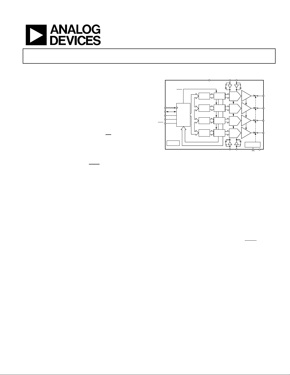
2.5 V to 5.5 V, 400 μA, 2-Wire Interface,
Quad Voltage Output, 8-/10-/12-Bit DACs
FEATURES
AD5306: 4 buffered, 8-bit DACs in 16-lead TSSOP
A version: ±1 LSB INL; B version: ±0.625 LSB INL
AD5316: 4 buffered, 10-bit DACs in 16-lead TSSOP
A version: ±4 LSB INL; B version: ±2.5 LSB INL
AD5326: 4 buffered, 12-bit DACs in 16-lead TSSOP
A version: ±16 LSB INL; B version: ±10 LSB INL
Low power operation: 400 μA @ 3 V, 500 μA @ 5 V
2-wire (I
2.5 V to 5.5 V power supply
Guaranteed monotonic by design over all codes
Power-down to 90 nA @ 3 V, 300 nA @ 5 V (
Double-buffered input logic
Buffered/unbuffered reference input options
Output range: 0 V to V
Power-on reset to 0 V
Simultaneous update of outputs (
Software clear facility
Data readback facility
On-chip rail-to-rail output buffer amplifiers
Temperature range −40°C to +105°C
APPLICATIONS
Portable battery-powered instruments
Digital gain and offset adjustment
Programmable voltage and current sources
Programmable attenuators
Industrial process control
1
Protected by U.S. Patent Numbers 5,969,657 and 5,684,481.
Rev. F
Information furnished by Analog Devices is believed to be accurate and reliable.
However, no responsibility is assumed by Analog Devices for its use, nor for any
infringements of patents or other rights of third parties that may result from its use.
Specifications subject to change without notice. No license is granted by implication
or otherwise under any patent or patent rights of Analog Devices. Trademarks and
registered trademarks are the property of their respective owners.
2
C®-compatible) serial interface
or 0 V to 2 V
REF
LDAC
REF
pin)
pin or bit)
PD
AD5306/AD5316/AD5326
FUNCTIONAL BLOCK DIAGRAM
V
BV
DAC
DAC
DAC
DAC
REF
REF
A
STRING
DAC A
STRING
DAC B
STRING
DAC C
STRING
DAC D
D
V
REF
REF
BUFFER
BUFFER
BUFFER
BUFFER
POWER-DOWN
CV
LDAC
V
DD
AD5306/AD5316/AD5326
LDAC
SCL
SDA
A1
A0
POWER-ON
RESET
LDAC
INTERFACE
LOGIC
INPUT
REGISTER
INPUT
REGISTER
INPUT
REGISTER
INPUT
REGISTER
REGISTER
REGISTER
REGISTER
REGISTER
Figure 1.
GENERAL DESCRIPTION
The AD5306/AD5316/AD53261 are quad 8-/10-/12-bit buffered
voltage output DACs in 16-lead TSSOP packages that operate
from a single 2.5 V to 5.5 V supply, consuming 500 μA at 3 V.
Their on-chip output amplifiers allow rail-to-rail output swing
with a slew rate of 0.7 V/μs. A 2-wire serial interface, which
operates at clock rates up to 400 kHz, is used. This interface is
SMBus-compatible at V
placed on the same bus.
Each DAC has a separate reference input that can be configured
as buffered or unbuffered. The outputs of all DACs can be
updated simultaneously using the asynchronous
The parts incorporate a power-on reset circuit that ensures the
DAC outputs power up to 0 V and remain there until a valid
write to the device takes place. The software clear function
clears all DACs to 0 V. The parts contain a power-down feature
that reduces the current consumption of the device to
300 nA @ 5 V (90 nA @ 3 V).
All three parts have the same pinout, which allows users to select
the amount of resolution appropriate for their application without
redesigning their circuit board.
One Technology Way, P.O. Box 9106, Norwood, MA 02062-9106, U.S.A.
Tel: 781.329.4700 www.analog.com
Fax: 781.461.3113 © 2005 Analog Devices, Inc. All rights reserved.
< 3.6 V. Multiple devices can be
DD
LOGIC
V
V
V
V
GNDPD
input.
A
OUT
B
OUT
C
OUT
D
OUT
02066-001

AD5306/AD5316/AD5326
TABLE OF CONTENTS
Specifications..................................................................................... 3
AC Characteristics........................................................................ 5
Timing Characteristics ................................................................ 6
Absolute Maximum Ratings............................................................ 7
ESD Caution.................................................................................. 7
Pin Configuration and Function Descriptions............................. 8
Te r mi n ol o g y ...................................................................................... 9
Typical Performance Characteristics ........................................... 11
Functional Description .................................................................. 15
Digital-to-Analog Section ......................................................... 15
Resistor String............................................................................. 15
DAC Reference Inputs ............................................................... 15
Output Amplifier........................................................................ 15
Power-On Reset .......................................................................... 16
Serial Interface............................................................................ 16
Read/Write Sequence................................................................. 16
Pointer Byte Bits ......................................................................... 16
Input Shift Register..................................................................... 16
Default Readback Conditions................................................... 17
Multiple DAC Write Sequence ................................................. 17
Multiple DAC Readback Sequence .......................................... 17
Write Operation.......................................................................... 18
Read Operation........................................................................... 18
Double-Buffered Interface........................................................ 19
Load DAC Input
Power-Down Mode .................................................................... 19
Applications..................................................................................... 20
Typical Application C i r c uit ....................................................... 20
Driving V
Bipolar Operation Using the AD5306/AD5316/AD5326..... 20
Multiple Devices on One Bus ................................................... 20
AD5306/AD5316/AD5326 as a Digitally Programmable
Window Detector....................................................................... 21
Coarse and Fine Adjustment Using the
AD5306/AD5316/AD5326 ....................................................... 21
Power Supply Decoupling ............................................................. 22
Outline Dimensions ....................................................................... 24
Ordering Guide .......................................................................... 24
LDAC
............................................................. 19
from the Reference Voltage ................................ 20
DD
REVISION HISTORY
8/05—Rev. E to Rev. F
Replaced Figure 22 .........................................................................13
Changes to Bipolar Operation
Using the AD5306/AD5316/AD5326 Section........................ 20
Changes to Ordering Guide.......................................................... 24
5/05—Rev. D to Rev. E
Changes to Table 1............................................................................ 3
11/04—Rev. C to Rev. D
Change to Figure 31 ....................................................................... 16
Changes to Pointer Byte Section................................................... 16
Change to Figure 32 ....................................................................... 17
Rev. F | Page 2 of 24
8/03—Rev. B to Rev. C
Added A Version ................................................................Universal
Changes to FEATURES ....................................................................1
Changes to SPECIFICATIONS .......................................................2
Changes to ABSOLUTE MAXIMUM RATINGS .........................5
Edits to ORDERING GUIDE ..........................................................5
Changes to TPC 21......................................................................... 11
Added OCTALS section to Table I............................................... 18
Updated OUTLINE DIMENSIONS ............................................ 19
4/01—Rev. A to Rev. B
Edit to Figure 6 ............................................................................... 13
Edits to RIGHT/LEFT section of Pointer Byte Bits section...... 13
Edits to Input Shift Register section ............................................ 13
Edits to Figure 7.............................................................................. 13
Edits to Figure 8.............................................................................. 14
Edits to Figure 9.............................................................................. 14
Edit to Figure 12 ............................................................................. 16
2/01—Rev. 0 to Rev. A
6/00—Revision 0: Initial Version

AD5306/AD5316/AD5326
SPECIFICATIONS
VDD = 2.5 V to 5.5 V; V
Table 1.
A Version
Parameter
DC PERFORMANCE
DAC REFERENCE INPUTS
OUTPUT CHARACTERISTICS
2
3, 4
AD5306
Resolution 8 8 Bits
Relative Accuracy ±0.15 ±1 ±0.15 ±0.625 LSB
Differential Nonlinearity ±0.02 ±0.25 ±0.02 ±0.25 LSB Guaranteed monotonic by
AD5316
Resolution 10 10 Bits
Relative Accuracy ±0.5 ±4 ±0.5 ±2.5 LSB
Differential Nonlinearity ±0.05 ±0.5 ±0.05 ±0.5 LSB Guaranteed monotonic by
AD5326
Resolution 12 12 Bits
Relative Accuracy ±2 ±16 ±2 ±10 LSB
Differential Nonlinearity ±0.2 ±1 ±0.2 ±1 LSB Guaranteed monotonic by
Offset Error ±5 ±60 ±5 ±60 mV VDD = 4.5 V, gain = 2;
Gain Error ±0.3 ±1.25 ±0.3 ±1.25 % of FSR VDD = 4.5 V, gain = 2;
Lower Deadband
Upper Deadband
Offset Error Drift
Gain Error Drift
6
6
DC Power Supply
Rejection Ratio
DC Crosstalk
V
REF
6
Input Range 1 V
0.25 V
V
Input Impedance >10 >10 MΩ Buffered reference mode
REF
148 180 148 180 kΩ Unbuffered reference mode;
74 90 74 90 kΩ Unbuffered reference mode;
Reference Feedthrough −90 −90 dB Frequency = 10 kHz.
Channel-to-Channel Isolation −75 −75 dB Frequency = 10 kHz.
Minimum Output Voltage
Maximum Output Voltage
DC Output Impedance 0.5 0.5 Ω
= 2 V; RL = 2 kΩ to GND; CL = 200 pF to GND; all specifications T
REF
1
Min Typ Max Min Typ Max Unit Conditions/Comments
5
5
10 60 10 60 mV See Figure 4; lower
10 60 10 60 mV See Figure 5; upper
−12 –12 ppm of FSR/°C
–5 –5 ppm of FSR/°C
6
–60 –60 dB ΔVDD = ±10%.
200 200 μV RL = 2 kΩ to GND or V
6
DD
DD
6
7
0.001 0.001 V This is a measure of the
7
V
− 0.001 VDD − 0.001 V
DD
1 V
0.25 V
B Version
to T
MIN
1
, unless otherwise noted.
MAX
design over all codes.
design over all codes.
design over all codes.
Figure 4 and Figure 5.
see
Figure 4 and Figure 5.
see
deadband exists only if
offset error is negative.
deadband exists only if
V
= VDD and offset plus
REF
gain error is positive.
DD.
DD
DD
V Buffered reference mode.
V Unbuffered reference mode.
and power-down mode.
0 V to V
0 V to 2 V
output range.
REF
output range.
REF
minimum and maximum
drive capability of the
output amplifier.
Rev. F | Page 3 of 24

AD5306/AD5316/AD5326
A Version
Parameter
2
Min Typ Max Min Typ Max Unit Conditions/Comments
1
B Version
1
Short-Circuit Current 25 25 mA VDD = 5 V.
16 16 mA VDD = 3 V.
Power-Up Time 2.5 2.5 μs Coming out of power-
down mode; V
= 5 V.
DD
5 5 μs Coming out of power-
= 3 V.
DD
LOGIC INPUTS
(Excluding SCL, SDA)
down mode; V
6
Input Current ±1 ±1 μA
VIL, Input Low Voltage 0.8 0.8 V VDD = 5 V ± 10%.
0.6 0.6 V VDD = 3 V ± 10%.
0.5 0.5 V VDD = 2.5 V.
VIH, Input High Voltage 1.7 1.7 V VDD = 2.5 V to 5.5 V;
TTL and 1.8 V CMOS
compatible.
Pin Capacitance 3 3 pF
LOGIC INPUTS (SCL, SDA)6
VIH, Input High Voltage 0.7 V
VIL, Input Low Voltage −0.3 +0.3 V
V
DD
+ 0.3 0.7 V
DD
DD
V
DD
+ 0.3 V SMBus compatible at
DD
V
DD
< 3.6 V.
−0.3 +0.3 VDDV SMBus compatible at
< 3.6 V.
V
DD
IIN, Input Leakage Current ±1 ±1 μA
V
, Input Hysteresis 0.05 VDD 0.05 VDD V See Figure 20.
HYST
CIN, Input Capacitance 8 8 pF
Glitch Rejection 50 50 ns Input filtering suppresses
noise spikes of less than
50 ns.
LOGIC OUTPUT (SDA)6
VOL, Output Low Voltage 0.4 0.4 V I
0.6 0.6 V I
= 3 mA.
SINK
= 6 mA.
SINK
Three-State Leakage Current ±1 ±1 μA
Three-State Output
8 8 pF
Capacitance
POWER REQUIREMENTS
V
DD
IDD (Normal Mode)
8
2.5 5.5 2.5 5.5 V
V
= VDD and VIL = GND;
IH
interface inactive.
VDD = 4.5 V to 5.5 V 500 900 500 900 μA All DACs in unbuffered
mode.
Buffered mode, extra
current is typically x mA
per DAC, where
x = 5 μA + V
REF/RDAC.
VDD = 2.5 V to 3.6 V 400 750 400 750 μA
IDD (Power-Down Mode) VIH = VDD and VIL = GND;
interface inactive.
VDD = 4.5 V to 5.5 V 0.3 1 0.3 1 μA IDD = 3 μA (max) during
readback on SDA.
VDD = 2.5 V to 3.6 V 0.09 1 0.09 1 μA IDD = 1.5 μA (max) during
readback on SDA.
1
Temperature range (A, B versions): −40°C to +105°C; typical at +25°C.
2
See the Terminology section.
3
DC specifications tested with the outputs unloaded.
4
Linearity is tested using a reduced code range: AD5306 (Code 8 to 255); AD5316 (Code 28 to 1023); AD5326 (Code 115 to 4095).
5
This corresponds to x codes. x = deadband voltage/LSB size.
6
Guaranteed by design and characterization; not production tested.
7
For the amplifier output to reach its minimum voltage, the offset error must be negative; for the amplifier output to reach its maximum voltage, V
the offset plus gain error must be positive.
8
Interface inactive; all DACs active. DAC outputs unloaded.
= VDD,
REF
Rev. F | Page 4 of 24

AD5306/AD5316/AD5326
AC CHARACTERISTICS
VDD = 2.5 V to 5.5 V; RL = 2 kΩ to GND; CL = 200 pF to GND; all specifications T
Table 2.
A, B Versions
Parameter
3
Min Typ Max Unit Conditions/Comments
1, 2
Output Voltage Settling Time V
AD5306 6 8 μs 1/4 scale to 3/4 scale change (0x40 to 0xC0)
AD5316 7 9 μs 1/4 scale to 3/4 scale change (0x100 to 0x300)
AD5326 8 10 μs 1/4 scale to 3/4 scale change (0x400 to 0xC00)
Slew Rate 0.7 V/μs
Major-Code Change Glitch Energy 12 nV-s 1 LSB change around major carry
Digital Feedthrough 0.5 nV-s
Digital Crosstalk 0.5 nV-s
Analog Crosstalk 1 nV-s
DAC-to-DAC Crosstalk 3 nV-s
Multiplying Bandwidth 200 kHz V
Total Harmonic Distortion −70 dB V
1
Guaranteed by design and characterization; not production tested.
2
Temperature range (A, B versions): −40°C to +105°C; typical at +25°C.
3
See the Terminology section.
MIN
to T
, unless otherwise noted.
MAX
= VDD = 5 V
REF
= 2 V ± 0.1 V p-p, unbuffered mode
REF
= 2.5 V ± 0.1 V p-p, frequency = 10 kHz
REF
Rev. F | Page 5 of 24
AD5306/AD5316/AD5326
A
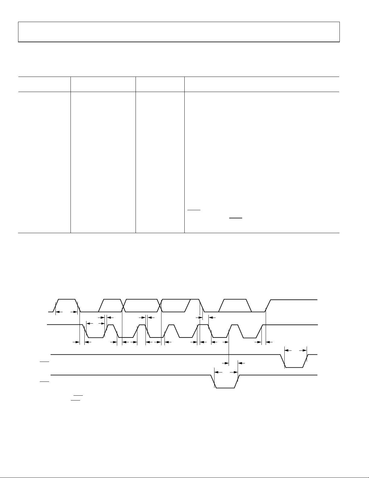
TIMING CHARACTERISTICS
VDD = 2.5 V to 5.5 V; all specifications T
Table 3.
Parameter
t
1
t
2
t
3
t
4
t
5
3
t
6
2
0 μs min
t
7
t
8
t
9
t
10
0 ns min tR, rise time of SCL and SDA when receiving (CMOS compatible)
t
11
0 ns min tF, fall time of SDA when receiving (CMOS compatible)
300 ns max tF, fall time of SCL and SDA when receiving
20 + 0.1C
t
12
t
13
4
C
B
1
See Figure 2.
2
Guaranteed by design and characterization; not production tested.
3
A master device must provide a hold time of at least 300 ns for the SDA signal (referred to the VIH min of the SCL signal) to bridge the undefined region of SCL’s
falling edge.
4
CB is the total capacitance of one bus line in pF. tR and tF measured between 0.3 VDD and 0.7 VDD.
Limit at T
2.5 μs min SCL cycle time
0.6 μs min t
1.3 μs min t
0.6 μs min t
100 ns min t
0.9 μs max t
0.6 μs min t
0.6 μs min t
1.3 μs min t
300 ns max tR, rise time of SCL and SDA when receiving
250 ns max tF, fall time of SDA when transmitting
20 ns min
400 ns min
400 pF max Capacitive load for each bus line
1
MIN
A, B Versions
, T
MIN
MAX
4
B
to T
, unless otherwise noted.
MAX
Unit Conditions/Comments
, SCL high time
HIGH
, SCL low time
LOW
, start/repeated start condition hold time
HD,STA
, data setup time
SU,DAT
, data hold time
HD,DAT
, setup time for repeated start
SU,STA
, stop condition setup time
SU,STO
, bus free time between a stop and a start condition
BUF
ns min tF, fall time of SCL and SDA when transmitting
LDAC pulse width
SCL rising edge to
LDAC rising edge
START
CONDITION
SD
t
9
t
3
SCL
t
4
1
LDAC
2
LDAC
NOTES
1
ASYNCHRONOUS LDAC UPDATE MODE.
2
SYNCHRONOUS LDAC UPDATE MODE.
t
10
t
6
t
11
t
2
t
5
Figure 2. 2-Wire Serial Interface Timing Diagram
REPEATED START
CONDITION
t
4
t
7
STOP
CONDITION
t
1
t
13
t
12
t
8
t
12
02066-002
Rev. F | Page 6 of 24
AD5306/AD5316/AD5326
ABSOLUTE MAXIMUM RATINGS
TA = 25°C, unless otherwise noted.
Table 4.
Parameter
VDD to GND −0.3 V to +7 V
SCL, SDA to GND −0.3 V to VDD + 0.3 V
A0, A1, LDAC, PD to GND
Reference Input Voltage to GND −0.3 V to VDD + 0.3 V
V
OUT
Operating Temperature Range
Industrial (A, B Versions) −40°C to +105°C
Storage Temperature Range −65°C to +150°C
Junction Temperature (TJ max) 150°C
16-Lead TSSOP
Power Dissipation (TJ max − TA)/θ
θJA Thermal Impedance 150.4°C/W
Reflow Soldering
Peak Temperature 220°C
Time at Peak Temperature 10 sec to 40 sec
1
Transient currents of up to 100 mA do not cause SCR latch-up.
A to V
1
D to GND −0.3 V to VDD + 0.3 V
OUT
Value
−0.3 V to V
+ 0.3 V
DD
JA
Stresses above those listed under Absolute Maximum Ratings
may cause permanent damage to the device. This is a stress
rating only; functional operation of the device at these or any
other conditions above those indicated in the operational
section of this specification is not implied. Exposure to absolute
maximum rating conditions for extended periods may affect
device reliability.
ESD CAUTION
ESD (electrostatic discharge) sensitive device. Electrostatic charges as high as 4000 V readily accumulate on the
human body and test equipment and can discharge without detection. Although this product features
proprietary ESD protection circuitry, permanent damage may occur on devices subjected to high energy
electrostatic discharges. Therefore, proper ESD precautions are recommended to avoid performance
degradation or loss of functionality.
Rev. F | Page 7 of 24
AD5306/AD5316/AD5326
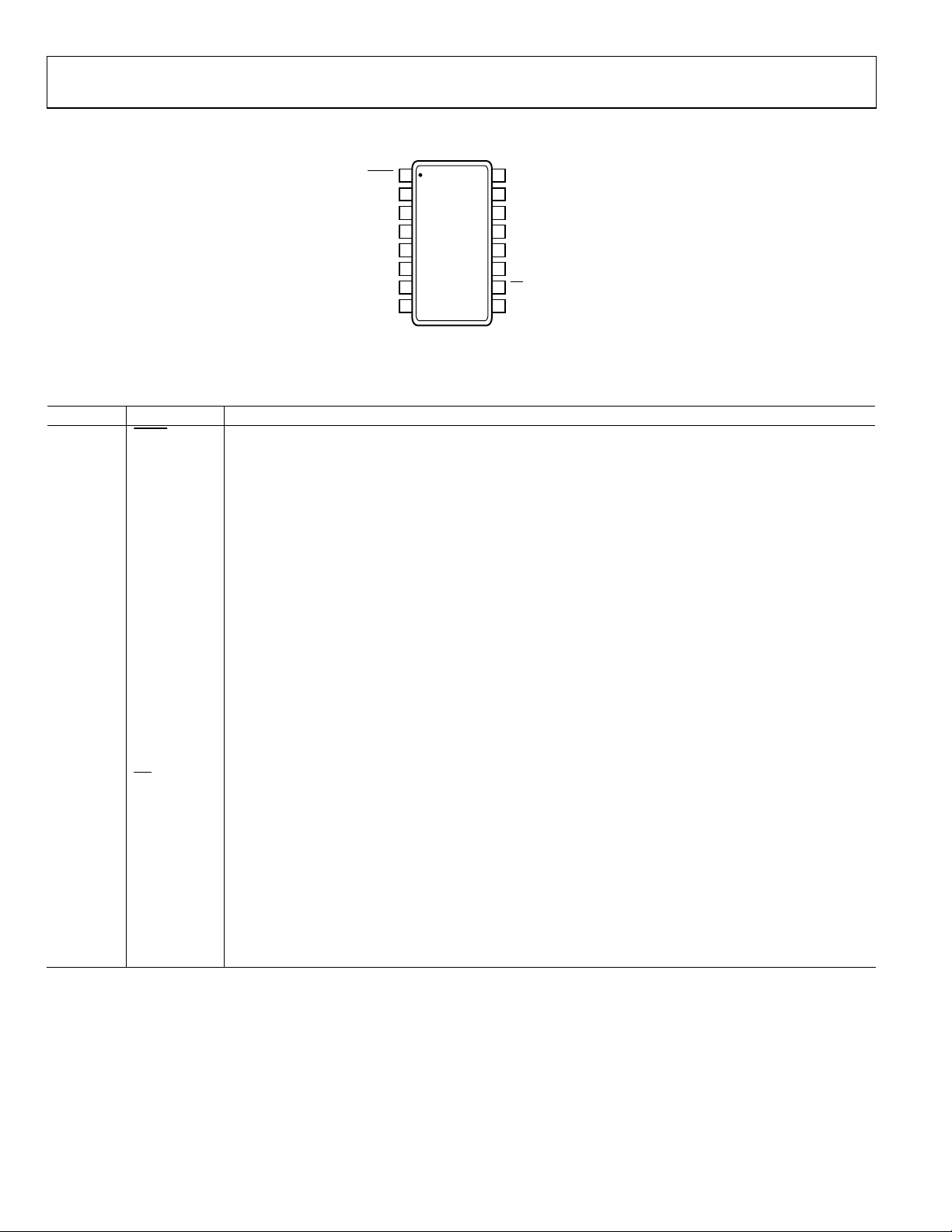
PIN CONFIGURATION AND FUNCTION DESCRIPTIONS
1
LDAC
2
V
DD
3
V
A
OUT
V
OUT
V
OUT
V
REF
V
REF
V
REF
AD5306/
4
AD5316/
B
AD5326
5
C
TOP VIEW
(Not to Scale)
6
A
7
B
8
CV
16
A1
15
A0
14
SCL
13
SDA
12
GND
11
D
V
OUT
10
PD
9
D
REF
02066-003
Figure 3. Pin Configuration
Table 5. Pin Function Descriptions
Pin No. Mnemonic Description
1
LDAC
Active Low Control Input. Transfers the contents of the input registers to their respective DAC registers.
Pulsing this pin low allows any or all DAC registers to be updated if the input registers have new data. This
allows simultaneous update of all DAC outputs. Alternatively, this pin can be tied permanently low.
2 V
DD
Power Supply Input. These parts can be operated from 2.5 V to 5.5 V and the supply should be decoupled
with a10 μF capacitor in parallel with a 0.1 μF capacitor to GND.
3 V
4 V
5 V
6 V
A Buffered Analog Output Voltage from DAC A. The output amplifier has rail-to-rail operation.
OUT
B Buffered Analog Output Voltage from DAC B. The output amplifier has rail-to-rail operation.
OUT
C Buffered Analog Output Voltage from DAC C. The output amplifier has rail-to-rail operation.
OUT
REF
A
Reference Input Pin for DAC A. This pin can be configured as a buffered or an unbuffered input depending on
the state of the BUF bit in the input word to DAC A. It has an input range from 0.25 V to V
7 V
REF
mode and from 1 V to V
B
Reference Input Pin for DAC B. This pin can be configured as a buffered or an unbuffered input depending on
in buffered mode.
DD
the state of the BUF bit in the input word to DAC B. It has an input range from 0.25 V to V
8 V
REF
mode and from 1 V to V
C
Reference Input Pin for DAC C. This pin can be configured as a buffered or an unbuffered input depending on
in buffered mode.
DD
the state of the BUF bit in the input word to DAC C. It has an input range from 0.25 V to V
9 V
REF
mode and from 1 V to V
D
Reference Input Pin for DAC D. This pin can be configured as a buffered or an unbuffered input depending on
in buffered mode.
DD
the state of the BUF bit in the input word to DAC D. It has an input range from 0.25 V to V
in buffered mode.
DD
10
mode and from 1 V to V
PD Active Low Control Input. Acts as a hardware power-down option. All DACs go into power-down mode when
this pin is tied low. The DAC outputs go into a high impedance state. The current consumption of the part
drops to 300 nA @ 5 V (90 nA @ 3 V).
11 V
D Buffered Analog Output Voltage from DAC D. The output amplifier has rail-to-rail operation.
OUT
12 GND Ground Reference Point for All Circuitry on the Part.
13 SDA
Serial Data Line. This is used in conjunction with the SCL line to clock data into the 16-bit input shift register.
It is a bidirectional open-drain data line that should be pulled to the supply with an external pull-up resistor.
14 SCL
Serial Clock Line. This is used in conjunction with the SDA line to clock data into the 16-bit input shift register.
Clock rates of up to 400 kbps can be accommodated in the I
15 A0 Address Input. Sets the LSB of the 7-bit slave address.
16 A1 Address Input. Sets the second LSB of the 7-bit slave address.
2
C-compatible interface.
in unbuffered
DD
in unbuffered
DD
in unbuffered
DD
in unbuffered
DD
Rev. F | Page 8 of 24
Loading...