


AD5346BCP
|
|
|
|
|
|
|
2.5 V to 5.5 V, Parallel Interface |
|
||||||||
|
|
|
|
|
|
Octal Voltage Output 8-/10-/12-Bit DACs |
|
|||||||||
|
|
|
|
|
|
|
|
|
|
|
|
|
|
|
|
|
|
|
|
|
|
|
|
AD5346/AD5347/AD5348 |
|
||||||||
|
|
|
|
|
|
|
|
|||||||||
|
|
|
|
|
|
|
|
|
|
|
|
|
|
|
|
|
FEATURES |
GENERAL DESCRIPTION |
|
||||||||||||||
AD5346: octal 8-bit DAC |
The AD5346/AD5347/AD53481 are octal 8-, 10-, and 12-bit |
|
||||||||||||||
AD5347: octal 10-bit DAC |
DACs, operating from a 2.5 V to 5.5 V supply. These devices |
|
||||||||||||||
AD5348: octal 12-bit DAC |
|
|||||||||||||||
incorporate an on-chip output buffer that can drive the output |
|
|||||||||||||||
Low power operation: 1.4 mA (max) @ 3.6 V |
|
|||||||||||||||
to both supply rails, and also allow a choice of buffered or |
|
|||||||||||||||
Power-down to 120 nA @ 3 V, 400 nA @ 5 V |
|
|||||||||||||||
unbuffered reference input. |
|
|||||||||||||||
Guaranteed monotonic by design over all codes |
|
|||||||||||||||
|
|
|
|
|
|
|
|
|
|
|||||||
Rail-to-rail output range: 0 V to VREF or 0 V to 2 × VREF |
The AD5346/AD5347/AD5348 have a parallel interface. |
CS |
|
|
||||||||||||
Power-on reset to 0 V |
selects the device and data is loaded into the input registers on |
|
||||||||||||||
Simultaneous update of DAC outputs via |
|
pin |
the rising edge of |
WR |
. A readback feature allows the internal |
|
||||||||||
LDAC |
|
|||||||||||||||
|
|
|
DAC registers to be read back through the digital port. |
|
||||||||||||
Asynchronous |
CLR |
facility |
|
|||||||||||||
Readback |
The GAIN pin on these devices allows the output range to be |
|
||||||||||||||
Buffered/unbuffered reference inputs |
|
|||||||||||||||
set at 0 V to VREF or 0 V to 2 × VREF. |
|
|||||||||||||||
|
|
|
|
|
|
|
|
|||||||||
20 ns WR time |
|
|||||||||||||||
Input data to the DACs is double-buffered, allowing simultane- |
|
|||||||||||||||
38-lead TSSOP/6 mm × 6 mm 40-lead LFCSP packaging |
|
|||||||||||||||
|
|
|
|
|
|
|
|
|
|
|||||||
ous update of multiple DACs in a system using the LDAC pin. |
|
|||||||||||||||
Temperature range: –40°C to +105°C |
|
|||||||||||||||
|
|
|
||||||||||||||
APPLICATIONS |
An asynchronous |
CLR |
input is also provided, which resets the |
|
||||||||||||
Portable battery-powered instruments |
contents of the input register and the DAC register to all zeros. |
|
||||||||||||||
These devices also incorporate a power-on reset circuit that |
|
|||||||||||||||
Digital gain and offset adjustment |
|
|||||||||||||||
ensures that the DAC output powers on to 0 V and remains |
|
|||||||||||||||
Programmable voltage and current sources |
|
|||||||||||||||
there until valid data is written to the device. |
|
|||||||||||||||
Optical networking |
|
|||||||||||||||
|
|
|
|
|
|
|
|
|
|
|||||||
Automatic test equipment |
All three parts are pin compatible, which allows users to select |
|
||||||||||||||
Mobile communications |
the amount of resolution appropriate for their application |
|
||||||||||||||
Programmable attenuators |
without redesigning their circuit board. |
|
||||||||||||||
Industrial process control |
|
|
|
|
|
|
|
|
|
|
||||||
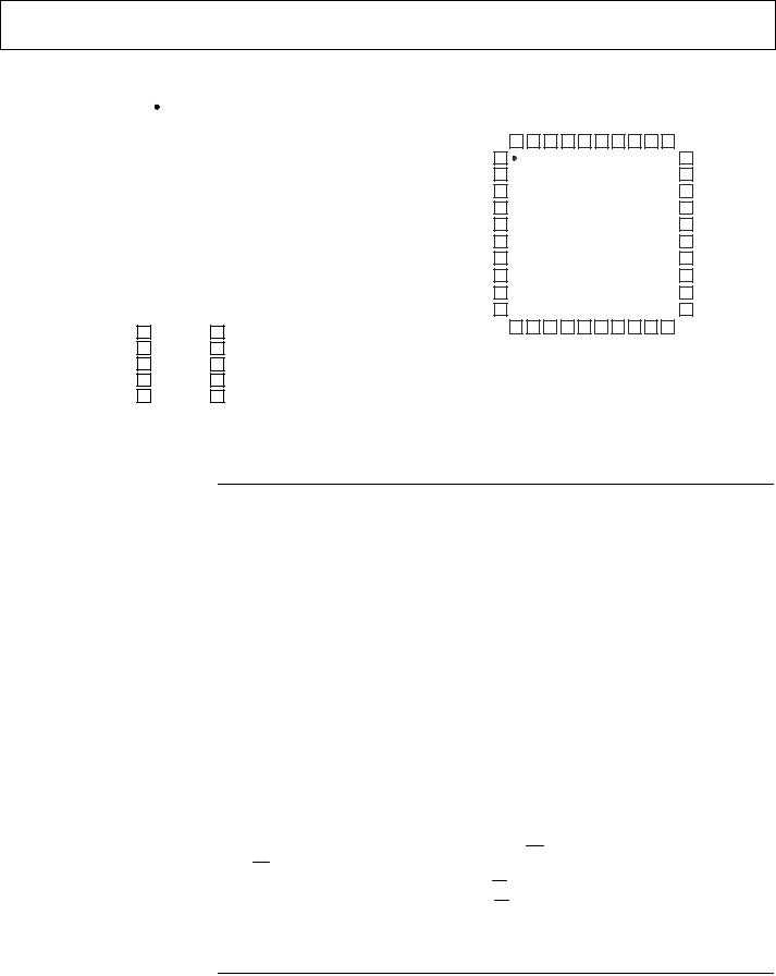
FUNCTIONAL BLOCK DIAGRAM
VDD |
AGND |
DGND |
VREFAB |
VREFCD |
|
||
|
AD5348 |
|
|
|
POWER-ON |
||
|
|
|
|
RESET |
|||
BUF |
INPUT |
|
DAC |
STRING |
|
|
|
GAIN |
REGISTER |
REGISTER |
BUFFER |
VOUTA |
|||
DAC A |
|||||||
DB11 |
INPUT |
|
DAC |
STRING |
|
|
|
. |
|
|
|
|
|
||
. |
REGISTER |
REGISTER |
DAC B |
BUFFER |
VOUTB |
||
. |
|||||||
DB0 |
INPUT |
|
DAC |
STRING |
|
|
|
|
|
BUFFER |
VOUTC |
||||
|
REGISTER |
REGISTER |
DAC C |
||||
CS |
INTER- |
INPUT |
DAC |
STRING |
BUFFER |
|
VOUTD |
RD |
FACE |
REGISTER |
REGISTER |
DAC D |
|
||
LOGIC |
INPUT |
DAC |
STRING |
|
|
|
|
WR |
|
BUFFER |
|
VOUTE |
|||
|
REGISTER |
REGISTER |
DAC E |
|
|||
A2 |
|
INPUT |
DAC |
STRING |
|
|
VOUTF |
|
REGISTER |
REGISTER |
DAC F |
BUFFER |
|
||
A1 |
|
INPUT |
DAC |
STRING |
BUFFER |
|
VOUTG |
|
|
REGISTER |
REGISTER |
DAC G |
|
||
A0 |
|
INPUT |
DAC |
STRING |
|
|
|
|
|
BUFFER |
|
VOUTH |
|||
|
|
REGISTER |
REGISTER |
|
|||
|
|
DAC H |
|
||||
CLR |
|
|
|
|
|
|
|
LDAC |
|
|
|
|
|
POWER-DOWN |
-001 |
|
|
|
|
|
LOGIC |
-0 |
|
|
|
|
|
|
|
03331 |
|
|
|
|
|
|
|
|
|
|
|
|
|
VREFGH |
VREFEF |
PD |
|
Figure 1.
1Protected by U.S. Patent No. 5,969,657; other patents pending.
Rev. 0
Information furnished by Analog Devices is believed to be accurate and reliable. However, no responsibility is assumed by Analog Devices for its use, nor for any infringements of patents or other rights of third parties that may result from its use. Specifications subject to change without notice. No license is granted by implication or otherwise under any patent or patent rights of Analog Devices. Trademarks and registered trademarks are the property of their respective owners.
One Technology Way, P.O. Box 9106, Norwood, MA 02062-9106, U.S.A. Tel: 781.329.4700 www.analog.com Fax: 781.326.8703 © 2003 Analog Devices, Inc. All rights reserved.

AD5346/AD5347/AD5348
TABLE OF CONTENTS |
|
Specifications..................................................................................... |
3 |
AC Characteristics............................................................................ |
4 |
Timing Characteristics..................................................................... |
5 |
Absolute Maximum Ratings............................................................ |
6 |
ESD Caution.................................................................................. |
6 |
AD5346 Pin Configurations and Function Descriptions ........... |
7 |
AD5347 Pin Configurations and Function Descriptions ........... |
8 |
AD5348 Pin Configurations and Function Descriptions ........... |
9 |
Terminology .................................................................................... |
10 |
Typical Performance Characteristics ........................................... |
12 |
Functional Description .................................................................. |
16 |
Digital-to-Analog Section ......................................................... |
16 |
Resistor String............................................................................. |
16 |
DAC Reference Input................................................................. |
16 |
Output Amplifier........................................................................ |
16 |
Parallel Interface ......................................................................... |
17 |
REVISION HISTORY |
|
Revision 0: Initial Version |
|
Power-On Reset.......................................................................... |
17 |
Power-Down Mode.................................................................... |
17 |
Suggested Data Bus Formats..................................................... |
18 |
Applications Information .............................................................. |
19 |
Typical Application Circuits ..................................................... |
19 |
Driving VDD from the Reference Voltage................................. |
19 |
Bipolar Operation Using the AD5346/AD5347/AD5348..... |
19 |
Decoding Multiple AD5346/AD5347/AD5348s.................... |
20 |
AD5346/AD5347/AD5348 as Digitally Programmable |
|
Window Detectors ...................................................................... |
20 |
Programmable Current Source ................................................ |
20 |
Coarse and Fine Adjustment Using the |
|
AD5346/AD5347/AD5348 ....................................................... |
21 |
Power Supply Bypassing and Grounding................................ |
21 |
Outline Dimensions ....................................................................... |
23 |
Ordering Guides......................................................................... |
24 |
Rev. 0 | Page 2 of 24

AD5346/AD5347/AD5348
SPECIFICATIONS
Table 1. VDD = 2.5 V to 5.5 V; VREF = 2 V; RL = 2 kΩ to GND; CL = 200 pF to GND; all specifications TMIN to TMAX, unless otherwise noted
|
|
B Version1 |
|
|
|
Parameter2 |
Min |
Typ |
Max |
Unit |
Conditions/Comments |
DC PERFORMANCE3,4 |
|
|
|
|
|
AD5346 |
|
|
|
|
|
Resolution |
|
8 |
|
Bits |
|
Relative Accuracy |
|
±0.15 |
±1 |
LSB |
|
Differential Nonlinearity |
|
±0.02 |
±0.25 |
LSB |
Guaranteed monotonic by design over all codes |
AD5347 |
|
|
|
|
|
Resolution |
|
10 |
|
Bits |
|
Relative Accuracy |
|
±0.5 |
±4 |
LSB |
|
Differential Nonlinearity |
|
±0.05 |
±0.5 |
LSB |
Guaranteed monotonic by design over all codes |
AD5348 |
|
|
|
|
|
Resolution |
|
12 |
|
Bits |
|
Relative Accuracy |
|
±2 |
±16 |
LSB |
|
Differential Nonlinearity |
|
±0.2 |
±1 |
LSB |
Guaranteed monotonic by design over all codes |
Offset Error |
|
±0.4 |
±3 |
% of FSR |
|
Gain Error |
|
±0.1 |
±1 |
% of FSR |
|
Lower Deadband5 |
|
10 |
60 |
mV |
Lower deadband exists only if offset error is negative |
Upper Deadband5 |
|
10 |
60 |
mV |
VDD = 5 V; upper deadband exists only if VREF = VDD |
Offset Error Drift6 |
|
–12 |
|
ppm of FSR/°C |
|
Gain Error Drift6 |
|
–5 |
|
ppm of FSR/°C |
|
DC Power Supply Rejection |
|
–60 |
|
dB |
∆VDD = ±10% |
Ratio6 |
|
|
|
|
|
DC Crosstalk6 |
|
200 |
|
µV |
RL = 2 kΩ to GND, 2 kΩ to VDD; CL = 200 pF to GND; |
|
|
|
|
|
Gain = +1 |
DAC REFERENCE INPUT6 |
|
|
|
|
|
VREF Input Range |
1 |
|
VDD |
V |
Buffered reference mode |
VREF Input Range |
0.25 |
|
VDD |
V |
Unbuffered reference mode |
VREF Input Impedance |
|
>10 |
|
MΩ |
Buffered reference mode and power-down mode |
|
|
90 |
|
kΩ |
Gain = +1; input impedance = RDAC |
|
|
45 |
|
kΩ |
Gain = +2; input impedance = RDAC |
Reference Feedthrough |
|
–90 |
|
dB |
Frequency = 10 kHz |
Channel-to-Channel Isolation |
|
–75 |
|
dB |
Frequency = 10 kHz |
|
|
|
|
|
|
OUTPUT CHARACTERISTICS6 |
|
|
|
|
|
Minimum Output Voltage4, 7 |
|
0.001 |
|
V min |
Rail-to-rail operation |
Maximum Output Voltage4, 7 |
|
VDD – |
|
V max |
|
|
|
0.001 |
|
|
|
DC Output Impedance |
|
0.5 |
|
Ω |
|
Short Circuit Current |
|
25 |
|
mA |
VDD = 5 V |
|
|
16 |
|
mA |
VDD = 3 V |
Power-Up Time |
|
2.5 |
|
µs |
Coming out of power-down mode; VDD = 5 V |
|
|
5 |
|
µs |
Coming out of power-down mode; VDD = 3 V |
|
|
|
|
|
|
LOGIC INPUTS |
|
|
|
|
|
Input Current |
|
|
±1 |
µA |
|
VIL, Input Low Voltage |
|
|
0.8 |
V |
VDD = 5 V ±10% |
|
|
|
0.7 |
V |
VDD = 3 V ±10% |
|
|
|
0.6 |
V |
VDD = 2.5 V |
VIH, Input High Voltage |
1.7 |
|
|
V |
VDD = 2.5 V to 5.5 V |
Pin Capacitance |
|
5 |
|
pF |
|
Rev. 0 | Page 3 of 24
AD5346/AD5347/AD5348
|
|
B Version1 |
|
|
|
Parameter2 |
Min |
Typ |
Max |
Unit |
Conditions/Comments |
LOGIC OUTPUTS6 |
|
|
|
|
|
VDD = 4.5 V to 5.5 V |
|
|
|
|
|
Output Low Voltage, VOL |
|
|
0.4 |
V |
ISINK = 200 µA |
Output High Voltage, VOH |
VDD – 1 |
|
|
V |
ISOURCE = 200 µA |
VDD = 2.5 V to 3.6 V |
|
|
|
|
|
Output Low Voltage, VOL |
|
|
0.4 |
V |
ISINK = 200 µA |
Output High Voltage, VOH |
VDD – 0.5 |
|
V |
ISOURCE = 200 µA |
|
POWER REQUIREMENTS |
|
|
|
|
|
VDD |
2.5 |
|
5.5 |
V |
|
IDD (Normal Mode) |
|
|
|
|
VIH = VDD, VIL = GND |
VDD = 4.5 V to 5.5 V |
|
1 |
1.65 |
mA |
All DACs in unbuffered mode. In buffered mode, |
VDD = 2.5 V to 3.6 V |
|
0.8 |
1.4 |
mA |
extra current is typically x µA per DAC, where x = 5 µA + |
|
|
|
|
|
VREF/RDAC |
IDD (Power-Down Mode) |
|
|
|
|
VIH = VDD, VIL = GND |
VDD = 4.5 V to 5.5 V |
|
0.4 |
1 |
µA |
|
VDD = 2.5 V to 3.6 V |
|
0.12 |
1 |
µA |
|
See footnotes after the AC Characteristics table.
AC CHARACTERISTICS6
Table 2. VDD = 2.5 V to 5.5 V; RL = 2 kΩ to GND; CL = 200 pF to GND; all specifications TMIN to TMAX, unless otherwise noted
|
|
|
B Version1 |
|
|
|
|
Parameter2 |
Min Typ |
Max |
Unit |
Conditions/Comments |
|
|
Output Voltage Settling Time |
|
|
|
|
VREF = 2 V |
|
AD5346 |
6 |
8 |
µs |
1/4 scale to 3/4 scale change (40 H to C0 H) |
|
|
AD5347 |
7 |
9 |
µs |
1/4 scale to 3/4 scale change (100 H to 300 H) |
|
|
AD5348 |
8 |
10 |
µs |
1/4 scale to 3/4 scale change (400 H to C00 H) |
|
|
Slew Rate |
0.7 |
|
V/µs |
|
|
|
Major Code Transition Glitch |
8 |
|
nV-s |
1 LSB change around major carry |
|
|
Energy |
|
||||
|
|
|
|
|
|
|
|
Digital Feedthrough |
0.5 |
|
nV-s |
|
|
|
Digital Crosstalk |
1 |
|
nV-s |
|
|
|
Analog Crosstalk |
1 |
|
nV-s |
|
|
|
DAC-to-DAC Crosstalk |
3.5 |
|
nV-s |
|
|
|
Multiplying Bandwidth |
200 |
|
kHz |
VREF = 2 V ±0.1 V p-p; unbuffered mode |
|
|
Total Harmonic Distortion |
|
–70 |
|
dB |
VREF = 2. V ±0.1 V p-p; frequency = 10 kHz; unbuffered mode |
|
|
|
|
|
|
|
1 Temperature range: B Version: –40°C to +105°C; typical specifications are at 25°C. 2 See Terminology section.
3 Linearity is tested using a reduced code range: AD5346 (Code 8 to 255); AD5347 (Code 28 to 1023); AD5348 (Code 115 to 4095). 4 DC specifications tested with outputs unloaded.
5 This corresponds to x codes. x = deadband voltage/LSB size.
6 Guaranteed by design and characterization, not production tested.
7For the amplifier output to reach its minimum voltage, offset error must be negative. For the amplifier output to reach its maximum voltage, VREF = VDD and the offset plus gain error must be positive.
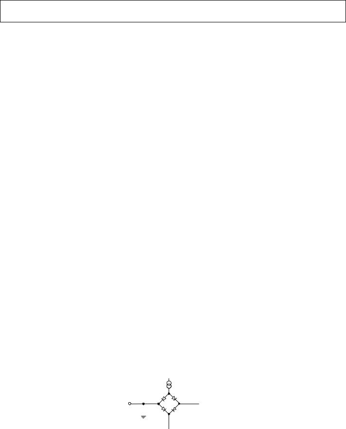
200µA |
IOL |
TO OUTPUT
PIN CL  50pF
50pF 
200µA  IOH
IOH
 VOH(min) + VOL(max)
2
03331-0-002
Figure 2. Load Circuit for Digital Output Timing Specifications
Rev. 0 | Page 4 of 24
AD5346/AD5347/AD5348
TIMING CHARACTERISTICS1, 2, 3
Table 3. VDD = 2.5 V to 5.5 V; all specifications TMIN to TMAX, unless otherwise noted
Parameter |
Limit at TMIN, TMAX |
Unit |
|
Condition/Comments |
|||||||||||||||||||||||||||||||||||||||||||
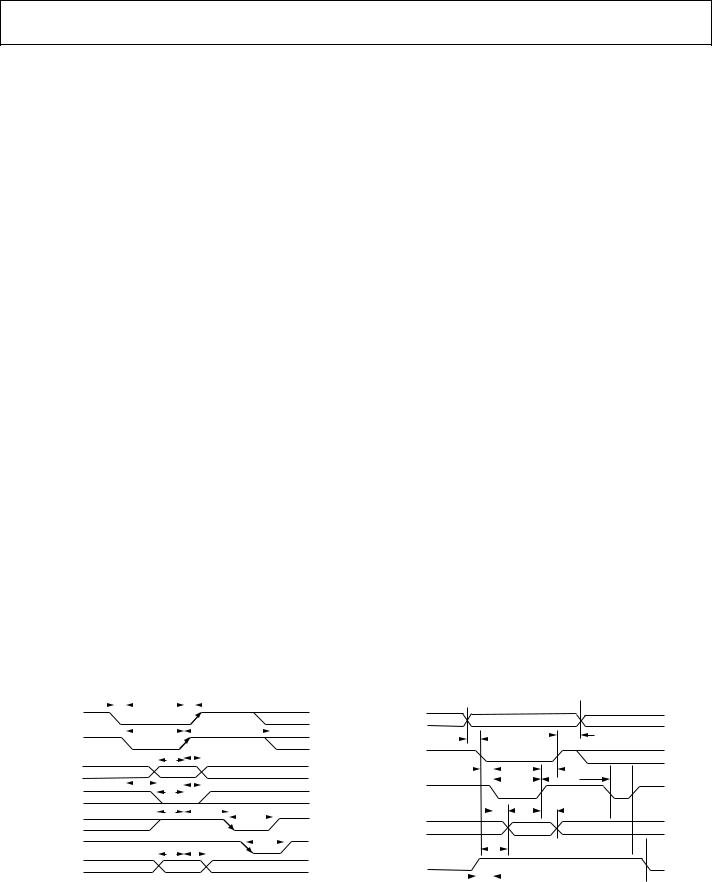
Data Write Mode (Figure 3) |
|
|
|
|
|
|
|
|
|
|
|
|
|
|
|
|
|
|
|
|
|
|
|
|
|
|
|
|
|
|
|
|
|
|
|
|
|
|
|
|
|
|
|
|
|
|
|
t1 |
0 |
ns min |
|
CS |
|
|
to |
WR |
setup time |
||||||||||||||||||||||||||||||||||||||
|
|
|
|
|
|
|
|
|
|
|
|
|
|
|
|
|
|
|
|
|
|
|
|
|
|
|
|
|
|
|
|
|
|
|
|
|
|
|
|
|
|
|
|
||||
t2 |
0 |
ns min |
|
CS |
|
to |
WR |
hold time |
|||||||||||||||||||||||||||||||||||||||
|
|
|
|
|
|
pulse width |
|||||||||||||||||||||||||||||||||||||||||
t3 |
20 |
ns min |
|
WR |
|
||||||||||||||||||||||||||||||||||||||||||
t4 |
5 |
ns min |
|
Data, GAIN, BUF setup time |
|||||||||||||||||||||||||||||||||||||||||||
t5 |
4.5 |
ns min |
|
Data, GAIN, BUF hold time |
|||||||||||||||||||||||||||||||||||||||||||
t6 |
5 |
ns min |
|
Synchronous mode. |
WR |
falling to |
LDAC |
falling. |
|||||||||||||||||||||||||||||||||||||||
|
|
|
|
|
|
|
|
|
|
|
|
|
|
|
|
|
|
|
|
|
|
|
|
|
|
|
|
|
|
|
|
|
|
|
|
|
|||||||||||
t7 |
5 |
ns min |
|
Synchronous mode. |
LDAC |
falling to |
WR |
rising. |
|||||||||||||||||||||||||||||||||||||||
t8 |
4.5 |
ns min |
|
Synchronous mode. |
WR |
rising to |
LDAC |
|
rising. |
||||||||||||||||||||||||||||||||||||||
|
|
|
|
|
|
|
|
|
|
|
|
|
|
|
|
|
|
|
|
|
|
|
|
|
|
|
|
|
|
|
|
||||||||||||||||
t9 |
5 |
ns min |
|
Asynchronous mode. |
|
LDAC |
rising to |
WR |
|
rising. |
|||||||||||||||||||||||||||||||||||||
|
|
|
|
|
|
|
|
|
|
|
|
|
|
|
|
|
|
|
|
|
|
|
|
|
|
|
|
||||||||||||||||||||
t10 |
4.5 |
ns min |
|
Asynchronous mode. |
WR |
rising to |
LDAC |
|
falling. |
||||||||||||||||||||||||||||||||||||||
|
|
|
|
|
|
|
|
|
|
|
|
|
|
|
|
|
|
|
|
|
|
|
|
|
|
||||||||||||||||||||||
t11 |
20 |
ns min |
|
LDAC |
pulse width |
||||||||||||||||||||||||||||||||||||||||||
|
|
|
|
|
|
|
|
|
|
|
|
|
|
|
|
|
|
|
|
|
|
|
|
|
|||||||||||||||||||||||
t12 |
10 |
ns min |
|
CLR |
pulse width |
||||||||||||||||||||||||||||||||||||||||||
|
|
|
|
|
|
|
|
|
|
|
|
|
|
|
|
|
|
|
|
|
|
|
|||||||||||||||||||||||||
t13 |
20 |
ns min |
|
Time between |
WR |
cycles |
|||||||||||||||||||||||||||||||||||||||||
t14 |
20 |
ns min |
|
A0, A1, A2 setup time |
|||||||||||||||||||||||||||||||||||||||||||
t15 |
0 |
ns min |
|
A0, A1, A2 hold time |
|||||||||||||||||||||||||||||||||||||||||||
Data Readback Mode (Figure 4) |
|
|
|
|
|
|
|
|
|
|
|
|
|
|
|
|
|
|
|
|
|
|
|
|
|
|
|
|
|
|
|
|
|
|
|
|
|
|
|
|
|
|
|
|
|
|
|
t16 |
0 |
ns min |
|
A0, A1, A2 to |
CS |
setup time |
|||||||||||||||||||||||||||||||||||||||||
t17 |
0 |
ns min |
|
A0, A1, A2 to |
CS |
hold time |
|||||||||||||||||||||||||||||||||||||||||
t18 |
0 |
ns min |
|
CS |
|
to falling edge of |
RD |
|
|
|
|
|
|||||||||||||||||||||||||||||||||||
|
|
|
|
|
|
|
|
|
|
|
|
|
|
|
|
|
|
||||||||||||||||||||||||||||||
t19 |
20 |
ns min |
|
RD |
pulse width; VDD = 3.6 V to 5.5 V |
||||||||||||||||||||||||||||||||||||||||||
|
|
|
|
|
|
|
|
|
|
|
|
|
|
|
|
|
|
||||||||||||||||||||||||||||||
|
30 |
ns min |
|
RD |
pulse width; VDD = 2.5 V to 3.6 V |
||||||||||||||||||||||||||||||||||||||||||
|
|
|
|
|
|
|
|
|
|
|
|
|
|
|
|
|
|
||||||||||||||||||||||||||||||
t20 |
0 |
ns min |
|
CS |
to |
RD |
hold time |
||||||||||||||||||||||||||||||||||||||||
t21 |
22 |
ns max |
|
Data access time after falling edge of |
RD; |
VDD = 3.6 V to 5.5 V |
|||||||||||||||||||||||||||||||||||||||||
|
|
|
|
|
|
|
|
|
|
|
|
|
|
|
|||||||||||||||||||||||||||||||||
|
30 |
ns max |
|
Data access time after falling edge of |
RD |
VDD = 2.5 V to 3.6 V |
|||||||||||||||||||||||||||||||||||||||||
|
|
|
|
|
|
|
|
|
|
|
|
|
|||||||||||||||||||||||||||||||||||
t22 |
4 |
ns min |
|
Bus relinquish time after rising edge of |
RD |
|
|||||||||||||||||||||||||||||||||||||||||
|
30 |
ns max |
|
|
|
|
|
|
|
|
|
|
|
|
|
|
|
|
|
|
|
|
|
|
|
|
|
|
|
|
|
|
|
|
|
|
|
|
|
|
|
|
|
|
|
|
|
t23 |
22 |
ns max |
|
CS |
falling edge to data; VDD = 3.6 V to 5.5 V |
||||||||||||||||||||||||||||||||||||||||||
|
|
|
|
|
|
|
|
|
|
|
|
|
|||||||||||||||||||||||||||||||||||
|
30 |
ns max |
|
CS |
falling edge to data; VDD = 2.5 V to 3.6 V |
||||||||||||||||||||||||||||||||||||||||||
|
|
|
|
|
|
|
|
|
|
|
|
||||||||||||||||||||||||||||||||||||
t24 |
30 |
ns min |
|
Time between |
RD |
cycles |
|||||||||||||||||||||||||||||||||||||||||
t25 |
30 |
ns min |
|
Time from |
RD |
|
to |
WR |
|
||||||||||||||||||||||||||||||||||||||
|
|
|
|
|
|
||||||||||||||||||||||||||||||||||||||||||
t26 |
30 |
ns min |
|
Time from |
WR |
to |
RD, |
VDD = 3.6 V to 5.5 V |
|||||||||||||||||||||||||||||||||||||||
|
|
|
|
|
|||||||||||||||||||||||||||||||||||||||||||
|
50 |
ns min |
|
Time from |
WR |
to |
RD, |
VDD = 2.5 V to 3.6 V |
|||||||||||||||||||||||||||||||||||||||
1 Guaranteed by design and characterization, not production tested.
2 All input signals are specified with tr = tf = 5 ns (10% to 90% of VDD) and timed from a voltage level of (VIL + VIH)/2. 3 See Figure 2.
|
|
|
|
|
|
|
|
|
|
t1 |
|
|
|
|
|
|
|
|
|
|
t2 |
|
|
|
|
|
|
|
|
|
|
|
|
|
|
|
|
|
|
|
A0–A2 |
|
|
|
|
|
|
|
|
|
|
|||||||||||||||||||||||
|
|
|
|
|
|
|
|
|
|
|
|
|
|
|
|
|
|
|
|
|
|
|
|
|
|
|
|
|
|
|
|
|
|
|
|
|
|
|
|
|
|
|
|
|
|
|
|
|
||||||||||||||||||||||||||
|
|
|
|
CS |
|
|
|
|
|
|
|
|
|
|
|
|
|
|
|
|
|
|
|
|
|
|
|
|
|
|
|
|
|
|
|
|
|
|
|
|
|
|
|
|
|
|
|
|
|
|
||||||||||||||||||||||||
|
|
|
|
|
|
|
|
|
|
|
|
|
|
|
|
|
t3 |
|
|
|
|
|
|
|
|
|
|
|
t13 |
|
|
|
|
|
|
|
|
|
|
|
|
|
|
|
|
|
|
t16 |
|
|
|
|
|
|
|
|
|
|
|
|
|
|
|
|
|
t17 |
||||||||
|
|
|
WR |
|
|
|
|
|
|
|
|
|
|
|
|
|
|
|
|
|
|
|
|
|
|
|
|
|
|
|
|
|
|
|
|
|
|
|
|
|
|
|
|
|
|
|
|
|
|
|
|
|
|
|
|
|
|
|
|
|
|
|
|
|
|
|
|
|
|
|
|
|||
|
|
|
|
|
|
|
|
|
|
|
|
|
|
|
|
|
|
|
|
|
|
|
|
|
t5 |
|
|
|
|
|
|
|
|
|
|
|
|
|
|
|
|
|
|
|
|
|
|
|
|
|
|
|
|
|
|
|
|
|
|
|
|
|
|
|
|
|
|
|
|
|
|
|||
|
|
|
|
|
|
|
|
|
|
|
|
|
|
|
|
|
|
t4 |
|
|
|
|
|
|
|
|
|
|
|
|
|
|
|
|
|
|
|
CS |
|
|
|
|
|
|
|
|
|
|
|
|
|
|
|
|
|
|
|
|
|
|
|
|
|
|
|
|
|
|||||||
|
DATA, |
|
|
|
|
|
|
|
|
|
|
|
|
|
|
|
|
|
|
|
|
|
|
|
|
|
|
|
|
|
|
|
|
|
|
|
|
|
|
|
|
|
|
|
|
|
|
t18 |
|
|
|
|
|
|
|
|
|
|
|
t20 |
|
|
|
|
||||||||||
|
|
|
|
|
|
|
|
|
|
|
|
|
|
|
|
|
|
|
|
|
|
|
|
|
|
|
|
|
|
|
|
|
|
|
|
|
|
|
|
|
|
|
|
|
|
|
|
|
|
|
|
|
|
|
|
|||||||||||||||||||
GAIN, BUF |
|
|
|
|
|
|
|
|
|
|
|
|
|
|
|
|
|
|
|
|
|
|
|
|
|
|
|
|
|
|
|
|
|
|
|
|
|
|
|
|
|
|
|
|
|
|
|
|
|
|
|
|
|
|
t19 |
|
|
|
|
|
|
|
|
t24 |
||||||||||
|
|
|
|
|
|
|
|
|
|
|
|
|
t6 |
t7 |
|
|
|
|
t8 |
|
|
|
|
|
|
|
|
|
|
|
|
|
|
|
|
|
|
|
|
|
|
|
|
|
|
|
|
|
|
|
|
|
|
|
|
|
|
|
|
|
|
|
|
|
|
|||||||||
|
|
|
|
|
|
|
|
|
|
|
|
|
|
|
|
|
|
|
|
|
|
|
|
|
|
|
|
|
|
|
|
|
|
|
|
|
|
|
|
|
|
|
|
|
|
|
|
|
|
|
|
|
|
|
|
|
|
|
|
|
|
|
|
|
|
|
|
|||||||
|
|
|
|
|
|
|
|
|
|
|
|
|
|
|
|
|
|
|
|
|
|
|
|
|
|
|
|
|
|
|
|
|
|
|
|
|
|
|
|
RD |
|
|
|
|
|
|
|
|
|
|
|
|
|
|
|
|
|
|
|
|||||||||||||||
LDAC1 |
|
|
|
|
|
|
|
|
|
|
|
|
|
|
|
|
|
|
|
|
|
|
|
|
|
|
|
|
|
|
|
|
|
|
|
|
|
|
|
|
|
|
|
|
|
|
|
|
|
|
|
|
||||||||||||||||||||||
|
|
|
|
|
|
|
|
|
|
|
|
|
|
|
|
|
|
|
|
|
|
|
|
|
|
|
|
|
|
|
|
|
|
|
|
|
|
|
|
|
|
|
|
|
|
|
|
|
|
|
|
|
|
|
||||||||||||||||||||
|
|
|
|
|
2 |
|
|
|
|
|
|
|
|
|
|
|
t9 |
|
|
|
|
t10 |
|
|
|
|
|
t11 |
|
|
|
|
|
|
|
|
|
|
|
|
|
|
|
|
|
|
|
|
|
|
|
t21 |
|
|
|
|
|
t22 |
|
|
|
|||||||||||||
|
|
|
|
|
|
|
|
|
|
|
|
|
|
|
|
|
|
|
|
|
|
|
|
|
|
|
|
|
|
|
|
|
|
|
|
|
|
|
|
|
|
|
|
|
|
|
|
|
|
|
|
|
|
|
|
|
|
|
|
|
|
|
|
|
|
|
|
|
|
|
||||
|
LDAC |
|
|
|
|
|
|
|
|
|
|
|
|
|
|
|
|
|
|
|
|
|
|
|
|
|
|
|
|
|
|
|
|
|
|
|
DATA |
|
|
|
|
|
|
|
|
|
|
|
|
|
|
|
|
|
|
|
||||||||||||||||||
|
|
|
|
|
|
|
|
|
|
|
|
|
|
|
|
|
|
|
|
|
|
|
|
|
|
|
|
|
|
|
|
|
|
|
|
|
|
|
|
|
|
|
|
|
||||||||||||||||||||||||||||||
|
|
|
|
|
|
|
|
|
|
|
|
|
|
|
|
|
|
|
|
|
|
|
|
|
|
|
|
|
|
|
|
|
|
|
t12 |
|
|
|
|
|
|
|
|
|
|
|
|
|
|
|
|
|
t |
|
23 |
|
|
|
|
|
|
|
|
|
|
|
|
|
|
|
|
|
||
|
|
|
|
|
|
|
|
|
|
|
|
|
|
|
|
|
|
|
|
|
|
|
|
|
|
|
|
|
|
|
|
|
|
|
|
|
|
|
|
|
|
|
|
|
|
|
|
|
|
|
|
|
|
|
|
|
|
|
|
|
|
|
|
|
|
|
|
|
|
|||||
|
|
|
|
|
|
|
|
|
|
|
|
|
|
|
|
|
|
|
|
|
|
|
|
|
|
|
|
|
|
|
|
|
|
|
|
|
|
|
|
|
|
|
|
|
|
|
||||||||||||||||||||||||||||
|
CLR |
|
|
|
|
|
|
|
|
|
|
|
t14 |
|
|
|
|
|
t15 |
|
|
|
|
|
|
|
|
|
|
|
|
|
|
|||||||||||||||||||||||||||||||||||||||||
|
|
|
|
|
|
|
|
|
|
|
|
|
|
|
|
|
|
|
|
|
|
|
|
|
|
|
|
|
|
|
|
|
|
|
|
|
|
|
|
|
|
|
|
|
|
|
|
|
|
|
|
|
|
|
|
|
|
|
|
|
|
|
||||||||||||
|
A0–A2 |
|
|
|
|
|
|
|
|
|
|
|
|
|
|
|
|
|
|
|
|
|
|
|
|
|
|
|
|
|
|
WR |
|
|
|
|
|
|
|
|
|
|
|
|
|
|
|
|
|
|
|
|
|
|
|
|||||||||||||||||||
|
|
|
|
|
|
|
|
|
|
|
|
|
|
|
|
|
|
|
|
|
|
|
|
|
|
|
|
|
|
|
|
|
|
|
|
|
|
|
|
|
|
|
|
|
|
|
|
|
|
|||||||||||||||||||||||||
|
|
|
|
|
|
|
|
|
|
|
|
|
|
|
|
|
|
|
|
|
|
|
|
|
|
|
|
|
|
|
|
|
|
|
|
|
|
|
|
|
|
|
|
|
|
t26 |
|
|
|
|
|
|
|
|
|
|
|
|
|
|
|
|
|
|
|
|||||||||
|
|
|
|
|
|
|
NOTES |
|
|
|
|
|
|
|
|
|
|
|
|
|
|
|
003 |
|
|
|
|
|
|
|
|
|
|
|
|
|
|
|
|
|
|
|
|
|
|
|
|
|
|
|
||||||||||||||||||||||||
|
|
|
|
|
|
|
|
|
|
|
|
|
|
|
|
|
|
|
|
|
|
|
|
|
|
|
|
|
|
|
|
|
|
|
|
|
|
|
|
|
|
|
||||||||||||||||||||||||||||||||
|
|
|
|
|
|
|
|
|
|
|
|
|
|
|
|
|
|
|
|
|
|
-0- |
|
|
|
|
|
|
|
|
|
|
|
|
|
|
|
|
|
|
|
|
|
|
|
|
|
|
|
|
|
|
|
|
|
|||||||||||||||||||
|
|
|
|
|
|
|
1. SYNCHRONOUS |
LDAC |
UPDATE MODE |
03331 |
|
|
|
|
|
|
|
|
|
|
|
|
|
|
|
|
|
|
|
|
|
|
|
|
|
|
|
|
|
|
|
|
|
|||||||||||||||||||||||||||||||
|
|
|
|
|
|
|
2. ASYNCHRONOUS LDAC UPDATE MODE |
|
|
|
|
|
|
|
|
|
|
|
|
|
|
|
|
|
|
|
|
|
|
|
|
|
|
|
|
|
|
|
|
|
||||||||||||||||||||||||||||||||||
 t25
t25
03331-0-004
Figure 3. Parallel Interface Write Timing Diagram |
Figure 4. Parallel Interface Read Timing Diagram |
Rev. 0 | Page 5 of 24

AD5346/AD5347/AD5348
ABSOLUTE MAXIMUM RATINGS
Table 4. TA = 25°C, unless otherwise noted
Parameter |
Rating |
|
|
|
|
VDD to GND |
–0.3 V to +7 V |
|
Digital Input Voltage to GND |
–0.3 V to VDD + 0.3 V |
|
Digital Output Voltage to GND |
–0.3 V to VDD + 0.3 V |
|
Reference Input Voltage to GND |
–0.3 V to VDD + 0.3 V |
|
VOUT to GND |
–0.3 V to VDD + 0.3 V |
|
Operating Temperature Range |
|
|
Industrial (B Version) |
–40°C to +105°C |
|
Storage Temperature Range |
–65°C to +150°C |
|
Junction Temperature |
150°C |
|
38-Lead TSSOP Package |
|
|
Power Dissipation |
(TJ max − TA)/ θJA mW |
|
θJA Thermal Impedance |
98.3°C/W |
|
θJC Thermal Impedance |
8.9°C/W |
|
40-Lead LFCSP Package |
|
|
Power Dissipation |
(TJ max − TA)/ θJA mW |
|
θJA Thermal Impedance (3-layer |
29.6°C/W |
|
board) |
||
|
||
Lead Temperature, Soldering (10 sec) |
300°C |
|
IR Reflow, Peak Temperature |
220°C |
Stresses above those listed under Absolute Maximum Ratings may cause permanent damage to the device. This is a stress rating only; functional operation of the device at these or any other conditions above those listed in the operational sections of this specification is not implied. Exposure to absolute maximum rating conditions for extended periods may affect device reliability.
ESD CAUTION
ESD (electrostatic discharge) sensitive device. Electrostatic charges as high as 4000 V readily accumulate on the human body and test equipment and can discharge without detection. Although this product features proprietary ESD protection circuitry, permanent damage may occur on devices subjected to high energy electrostatic discharges. Therefore, proper ESD precautions are recommended to avoid performance degradation or loss of functionality.
Rev. 0 | Page 6 of 24
AD5346/AD5347/AD5348
AD5346 PIN CONFIGURATIONS AND FUNCTION DESCRIPTIONS
VREFGH |
|
|
|
|
|
|
|
|
|
|
|||
1 |
|
38 |
|
PD |
|
|
|
||||||
VREFEF |
|
|
|
|
|
|
|
|
|
|
|||
2 |
|
37 |
|
CLR |
|
||||||||
VREFCD |
|
|
|
|
|
|
|
|
|
|
|||
3 |
|
36 |
GAIN |
||||||||||
|
VDD |
4 |
|
35 |
|
|
|
|
|||||
|
WR |
||||||||||||
VREFAB |
|
|
|
|
|
|
|
|
|
|
|||
5 |
|
34 |
|
RD |
|
|
|||||||
VOUTA |
|
|
|
|
|
|
|
|
|
|
|||
6 |
8-BIT |
33 |
|
CS |
|
||||||||
VOUTB |
|
AD5346 |
|
DB7 |
|||||||||
7 |
32 |
||||||||||||
VOUTC |
|
TOP VIEW |
|
DB6 |
|||||||||
8 |
(Not to Scale) |
31 |
|||||||||||
|
|
||||||||||||
VOUTD |
9 |
|
30 |
DB5 |
|||||||||
|
|
|
|
|
|
DB4 |
|||||||
AGND |
10 |
|
29 |
||||||||||
VOUTE |
11 |
|
28 |
DB3 |
|||||||||
V |
|
|
|
|
|
DB2 |
|||||||
F |
12 |
|
27 |
||||||||||
|
OUT |
|
|
|
|
|
DB1 |
||||||
|
|
|
|
|
|
||||||||
VOUTG |
13 |
|
26 |
||||||||||
|
|
|
|||||||||||
VOUTH |
14 |
|
25 |
DB0 |
|||||||||
|
|
||||||||||||
DGND 15 |
|
24 |
DGND |
||||||||||
|
BUF 16 |
|
23 |
DGND |
|||||||||
|
|
17 |
|
22 |
DGND |
||||||||
LDAC |
|
||||||||||||
|
A0 |
18 |
|
21 |
DGND |
||||||||
|
A1 |
19 |
|
20 |
A2 |
||||||||
|
|
|
|
|
|
|
|
|
|
|
|
|
|
03331-0-005
|
|
AB |
V |
V |
CD |
EF |
GH |
PD |
CLR |
GAIN |
WR |
|
|
|
|
|||
|
|
V |
V |
V |
V |
|
|
|
|
|||||||||
|
|
REF |
DD |
|
DD |
REF |
REF |
REF |
|
|
|
|
|
|
|
|
|
|
|
40 |
39 |
38 |
37 |
36 |
35 |
34 |
33 |
32 |
31 |
|
|
|
|
|
|||
VOUTA |
1 |
|
|
|
|
|
|
|
|
|
|
|
|
30 |
|
|
|
|
|
|
|
|
|
|
|
|
|
|
|
|
RD |
||||||
VOUTB |
2 |
|
|
|
|
|
|
|
|
|
|
|
|
29 |
|
|
||
|
|
|
|
|
|
|
|
|
|
|
|
CS |
||||||
VOUTC |
3 |
|
|
|
|
|
|
|
|
|
|
|
|
28 |
DB7 |
|||
VOUTD |
4 |
|
|
|
|
|
8-BIT |
|
|
|
|
|
27 |
DB6 |
||||
AGND 5 |
|
|
|
|
|
|
|
|
|
|
26 |
DB5 |
||||||
|
|
|
|
|
AD5346 |
|
|
|
|
|||||||||
AGND |
6 |
|
|
|
|
|
TOP VIEW |
|
|
|
|
25 |
DB4 |
|||||
VOUTE |
7 |
|
|
|
|
(Not to Scale) |
|
|
|
|
24 |
DB3 |
||||||
|
|
|
|
|
|
|
|
|
|
|
|
|||||||
VOUTF |
8 |
|
|
|
|
|
|
|
|
|
|
|
|
23 |
DB2 |
|||
VOUTG |
9 |
|
|
|
|
|
|
|
|
|
|
|
|
22 |
DB1 |
|||
VOUTH 10 |
|
|
|
|
|
|
|
|
|
|
|
|
21 |
DB0 |
||||
|
11 |
12 |
13 |
14 |
15 |
16 |
17 |
18 |
19 |
20 |
|
03331-0-006 |
||||||
|
|
DGND |
BUF |
|
LDAC |
A0 |
A1 |
A2 |
DGND |
DGND |
DGND |
|
DGND |
|||||
|
|
|
|
|||||||||||||||
|
|
|
|
|
|
|
|
|||||||||||
Figure 6. AD5346 Pin Configuration—LFCSP
Figure 5. AD5346 Pin Configuration—TSSOP
Table 5. AD5346 Pin Function Descriptions
Pin Number |
|
|
|
|
|
|
|
|
|
|
|
|
|
|
|
|
|
|
|
TSSOP |
LFCSP |
|
Mnemonic |
||||||
|
|
|
|
|
|
|
|
|
|
1 |
35 |
|
VREFGH |
||||||
2 |
36 |
|
VREFEF |
||||||
3 |
37 |
|
VREFCD |
||||||
4 |
38, 39 |
|
VDD |
||||||
5 |
40 |
|
VREFAB |
||||||
6–9, |
1–4, |
|
VOUTX |
||||||
11–14 |
7–10 |
|
|
|
|
|
|
|
|
10 |
5, 6 |
|
AGND |
||||||
15, |
11, |
|
DGND |
||||||
21–24 |
17–20 |
|
|
|
|
|
|
|
|
16 |
12 |
BUF |
|||||||
17 |
13 |
|
|
|
|
|
|
|
|
|
LDAC |
|
|||||||
18 |
14 |
A0 |
|||||||
19 |
15 |
A1 |
|||||||
20 |
16 |
A2 |
|||||||
25–32 |
21–28 |
|
DB0–DB7 |
||||||
33 |
29 |
|
|
|
|
|
|
||
|
CS |
|
|
|
|
|
|||
34 |
30 |
|
|
|
|
|
|||
|
RD |
|
|
|
|||||
35 |
31 |
|
|
|
|
||||
|
WR |
|
|
||||||
36 |
32 |
GAIN |
|||||||
37 |
33 |
|
|
|
|||||
|
CLR |
|
|||||||
38 |
34 |
|
|
||||||
|
PD |
|
|||||||
|
|
|
|
|
|
|
|
|
|
Function
Reference Input for DACs G and H. Reference Input for DACs E and F. Reference Input for DACs C and D.
Power Supply Pin(s). This part can operate from 2.5 V to 5.5 V, and the supply should be decoupled with a 10 µF capacitor in parallel with a 0.1 µF capacitor to GND. Both VDD pins on the LFCSP package must be at the same potential.
Reference Input for DACs A and B.
Output of DAC X. Buffered output with rail-to-rail operation.
Analog Ground. Ground reference for analog circuitry.
Digital Ground. Ground reference for digital circuitry.
Buffer Control Pin. Controls whether the reference input to the DAC is buffered or unbuffered.
Active Low Control Input. Updates the DAC registers with the contents of the input registers, which allows all DAC outputs to be simultaneously updated.
LSB Address Pin. Selects which DAC is to be written to. Address Pin. Selects which DAC is to be written to. MSB Address Pin. Selects which DAC is to be written to.
Eight Parallel Data Inputs. DB7 is the MSB of these eight bits.
Active Low Chip Select Input. Used in conjunction with WR to write data to the parallel interface, or with RD to read back data from a DAC.
Active Low Read Input. Used in conjunction with CS to read data back from the internal DACs. Active Low Write Input. Used in conjunction with CS to write data to the parallel interface.
Gain Control Pin. Controls whether the output range from the DAC is 0 V to VREF or 0 V to 2 × VREF. Asynchronous Active Low Control Input. Clears all input registers and DAC registers to zeros. Power-Down Pin. This active low control pin puts all DACs into power-down mode.
Rev. 0 | Page 7 of 24
AD5346/AD5347/AD5348
AD5347 PIN CONFIGURATIONS AND FUNCTION DESCRIPTIONS
VREFGH |
|
|
|
|
|
|
|
|
|
|||
1 |
|
38 |
|
PD |
|
|
||||||
VREFEF |
|
|
|
|
|
|
|
|
|
|||
2 |
|
37 |
|
CLR |
|
|||||||
VREFCD |
|
|
|
|
|
|
|
|
|
|||
3 |
|
36 |
GAIN |
|||||||||
|
VDD |
4 |
|
35 |
|
|
|
|
||||
|
WR |
|||||||||||
VREFAB |
|
|
|
|
|
|
|
|
|
|||
5 |
|
34 |
|
RD |
|
|
||||||
VOUTA |
|
|
|
|
|
|
|
|
|
|||
6 |
10-BIT |
33 |
|
CS |
|
|||||||
VOUTB |
|
AD5347 |
|
DB9 |
||||||||
7 |
32 |
|||||||||||
VOUTC |
|
TOP VIEW |
|
DB8 |
||||||||
8 |
(Not to Scale) |
31 |
||||||||||
|
|
|||||||||||
VOUTD |
9 |
|
30 |
DB7 |
||||||||
|
|
|
|
|
|
DB6 |
||||||
AGND |
10 |
|
29 |
|||||||||
VOUTE |
11 |
|
28 |
DB5 |
||||||||
|
|
|
|
|
|
DB4 |
||||||
VOUTF |
12 |
|
27 |
|||||||||
|
|
|
|
|
|
|
DB3 |
|||||
V |
G |
13 |
|
26 |
||||||||
|
OUT |
|
|
|
|
|
DB2 |
|||||
|
|
|
|
|
||||||||
VOUTH |
14 |
|
25 |
|||||||||
|
|
|||||||||||
DGND 15 |
|
24 |
DB1 |
|||||||||
|
BUF 16 |
|
23 |
DB0 |
||||||||
|
|
17 |
|
22 |
DGND |
|||||||
LDAC |
|
|||||||||||
|
A0 |
18 |
|
21 |
DGND |
|||||||
|
A1 |
19 |
|
20 |
A2 |
|||||||
|
|
|
|
|
|
|
|
|
|
|
|
|
03331-0-007
|
|
AB |
V |
V |
CD |
EF |
GH |
PD |
CLR |
GAIN |
WR |
|
|
|
|
|||
|
|
V |
V |
V |
V |
|
|
|
|
|||||||||
|
|
REF |
DD |
|
DD |
REF |
REF |
REF |
|
|
|
|
|
|
|
|
|
|
|
40 |
39 |
38 |
37 |
36 |
35 |
34 |
33 |
32 |
31 |
|
|
|
|
|
|||
VOUTA |
1 |
|
|
|
|
|
|
|
|
|
|
|
|
30 |
|
|
|
|
|
|
|
|
|
|
|
|
|
|
|
|
RD |
||||||
VOUTB |
2 |
|
|
|
|
|
|
|
|
|
|
|
|
29 |
|
|
||
|
|
|
|
|
|
|
|
|
|
|
|
CS |
||||||
VOUTC |
3 |
|
|
|
|
|
|
|
|
|
|
|
|
28 |
DB9 |
|||
VOUTD |
4 |
|
|
|
|
|
10-BIT |
|
|
|
|
|
27 |
DB8 |
||||
AGND 5 |
|
|
|
|
|
|
|
|
|
|
26 |
DB7 |
||||||
|
|
|
|
|
AD5347 |
|
|
|
|
|||||||||
AGND |
6 |
|
|
|
|
|
TOP VIEW |
|
|
|
|
25 |
DB6 |
|||||
VOUTE |
7 |
|
|
|
|
(Not to Scale) |
|
|
|
|
24 |
DB5 |
||||||
|
|
|
|
|
|
|
|
|
|
|
|
|||||||
VOUTF |
8 |
|
|
|
|
|
|
|
|
|
|
|
|
23 |
DB4 |
|||
VOUTG |
9 |
|
|
|
|
|
|
|
|
|
|
|
|
22 |
DB3 |
|||
VOUTH 10 |
|
|
|
|
|
|
|
|
|
|
|
|
21 |
DB2 |
||||
|
11 |
12 |
13 |
14 |
15 |
16 |
17 |
18 |
19 |
20 |
|
03331-0-008 |
||||||
|
|
DGND |
BUF |
|
LDAC |
A0 |
A1 |
A2 |
DGND |
DGND |
DB |
|
DB |
|||||
|
|
|
|
|
|
|
|
|
|
|
0 |
1 |
|
|
|
|
|
|
|
|
|
|
|
|
|
|
|
|
|
|
|
|
|
|
|
|
|
Figure 8. AD5347 Pin Configuration—LFCSP
Figure 7. AD5347 Pin Configuration—TSSOP
Table 6. AD5347 Pin Function Descriptions
Pin Number |
|
|
|
|
|
|
|
|
|
|
|
|
|
|
|
|
|
|
|
TSSOP |
LFCSP |
|
Mnemonic |
||||||
|
|
|
|
|
|
|
|
|
|
1 |
35 |
|
VREFGH |
||||||
2 |
36 |
|
VREFEF |
||||||
3 |
37 |
|
VREFCD |
||||||
4 |
38, 39 |
|
VDD |
||||||
5 |
40 |
|
VREFAB |
||||||
6–9, |
1–4, |
|
VOUTX |
||||||
11–14 |
7–10 |
|
|
|
|
|
|
|
|
10 |
5, 6 |
|
AGND |
||||||
15, 21–22 |
11, |
|
DGND |
||||||
|
17–18 |
|
|
|
|
|
|
|
|
16 |
12 |
BUF |
|||||||
17 |
13 |
|
|
|
|
|
|
|
|
|
LDAC |
|
|||||||
18 |
14 |
|
A0 |
||||||
19 |
15 |
A1 |
|||||||
20 |
16 |
A2 |
|||||||
23–32 |
19–28 |
|
DB0–DB9 |
||||||
33 |
29 |
|
|
|
|
|
|
||
|
CS |
|
|
|
|
|
|||
34 |
30 |
|
|
|
|
|
|||
|
RD |
|
|
|
|||||
35 |
31 |
|
|
|
|
||||
|
WR |
|
|
||||||
36 |
32 |
|
GAIN |
||||||
37 |
33 |
|
|
|
|||||
|
CLR |
|
|||||||
38 |
34 |
|
|
||||||
|
PD |
|
|||||||
|
|
|
|
|
|
|
|
|
|
Function
Reference Input for DACs G and H. Reference Input for DACs E and F. Reference Input for DACs C and D.
Power Supply Pin(s). This part can operate from 2.5 V to 5.5 V, and the supply should be decoupled with a 10 µF capacitor in parallel with a 0.1 µF capacitor to GND. Both VDD pins on the LFCSP package must be at the same potential.
Reference Input for DACs A and B.
Output of DAC X. Buffered output with rail-to-rail operation.
Analog Ground. Ground reference for analog circuitry.
Digital Ground. Ground reference for digital circuitry.
Buffer Control Pin. Controls whether the reference input to the DAC is buffered or unbuffered.
Active Low Control Input. Updates the DAC registers with the contents of the input registers, which allows all DAC outputs to be simultaneously updated.
LSB Address Pin. Selects which DAC is to be written to. Address Pin. Selects which DAC is to be written to. MSB Address Pin. Selects which DAC is to be written to.
Ten Parallel Data Inputs. DB9 Is the MSB of these ten bits.
Active Low Chip Select Input. Used in conjunction with WR to write data to the parallel interface, or with RD to read back data from a DAC.
Active Low Read Input. Used in conjunction with CS to read data back from the internal DACs. Active Low Write Input. Used in conjunction with CS to write data to the parallel interface.
Gain Control Pin. Controls whether the output range from the DAC is 0 V to VREF or 0 V to 2 × VREF. Asynchronous Active Low Control Input. Clears all input registers and DAC registers to zeros. Power-Down Pin. This active low control pin puts all DACs into power-down mode.
Rev. 0 | Page 8 of 24
 Loading...