


 Loading...
2.5 V to 5.5 V Octal Voltage Output 8-/10-/12-Bit DACs in 16-Lead TSSOP
FEATURES
AD5308: 8 buffered 8-bit DACs in 16-lead TSSOP A version: ±1 LSB INL, B version: ±0.75 LSB INL AD5318: 8 buffered 10-bit DACs in 16-lead TSSOP
A version: ±4 LSB INL, B version: ±3 LSB INL AD5328: 8 buffered 12-bit DACs in 16-lead TSSOP A version: ±16 LSB INL, B version: ±12 LSB INL
Low power operation: 0.7 mA @ 3 V Guaranteed monotonic by design over all codes Power-down to 120 nA @ 3 V, 400 nA @ 5 V Double-buffered input logic
Buffered/unbuffered/VDD reference input options Output range: 0 V to VREF or 0 V to 2 VREF Power-on reset to 0 V
Programmability
Individual channel power-down Simultaneous update of outputs (LDAC)
Low power, SPI-®, QSPI-™, MICROWIRE-™, and DSPcompatible 3-wire serial interface
On-chip rail-to-rail output buffer amplifiers Temperature range: −40°C to +125°C Qualified for automotive applications
GENERAL DESCRIPTION
The AD5308/AD5318/AD5328 are octal 8-, 10-, and 12-bit buffered voltage output DACs in a 16-lead TSSOP. They operate from a single 2.5 V to 5.5 V supply, consuming 0.7 mA typical at 3 V. Their on-chip output amplifiers allow the outputs to swing rail-to-rail with a slew rate of 0.7 V/μs. The AD5308/ AD5318/AD5328 use a versatile 3-wire serial interface that operates at clock rates up to 30 MHz and is compatible with standard SPI, QSPI, MICROWIRE, and DSP interface standards.
The references for the eight DACs are derived from two reference pins (one per DAC quad). These reference inputs can be configured as buffered, unbuffered, or VDD inputs. The parts
Rev. F
Information furnished by Analog Devices is believed to be accurate and reliable. However, no responsibilityisassumedbyAnalogDevicesforitsuse,norforanyinfringementsofpatentsorother rightsofthirdpartiesthatmayresultfromitsuse.Specificationssubjecttochangewithoutnotice.No license is granted by implication or otherwise under any patent or patent rights of Analog Devices. Trademarksandregisteredtrademarksarethepropertyoftheirrespectiveowners.
AD5308/AD5318/AD5328
APPLICATIONS
Portable battery-powered instruments
Digital gain and offset adjustment
Programmable voltage and current sources
Optical networking
Automatic test equipment
Mobile communications
Programmable attenuators
Industrial process control
incorporate a power-on reset circuit, which ensures that the DAC outputs power up to 0 V and remain there until a valid write to the device takes place. The outputs of all DACs may be updated simultaneously using the asynchronous LDAC input. The parts contain a power-down feature that reduces the current consumption of the devices to 400 nA at 5 V (120 nA at 3 V). The eight channels of the DAC may be powered down individually.
All three parts are offered in the same pinout, which allows users to select the resolution appropriate for their application without redesigning their circuit board.
One Technology Way, P.O. Box 9106, Norwood, MA 02062-9106, U.S.A. Tel: 781.329.4700 www.analog.com Fax: 781.461.3113 ©2002–2011 Analog Devices, Inc. All rights reserved.

AD5308/AD5318/AD5328
TABLE OF CONTENTS |
|
Features .............................................................................................. |
1 |
Applications....................................................................................... |
1 |
General Description ......................................................................... |
1 |
Revision History ............................................................................... |
2 |
Functional Block Diagram .............................................................. |
3 |
Specifications..................................................................................... |
4 |
Absolute Maximum Ratings............................................................ |
7 |
ESD Caution.................................................................................. |
7 |
Pin Configuration and Function Descriptions............................. |
8 |
Typical Performance Characteristics ............................................. |
9 |
Terminology .................................................................................... |
13 |
Theory of Operation ...................................................................... |
15 |
Digital-to-Analog Converter .................................................... |
15 |
Resistor String............................................................................. |
15 |
Output Amplifier........................................................................ |
15 |
Power-On Reset .......................................................................... |
16 |
Power-Down Mode .................................................................... |
16 |
Serial Interface ............................................................................ |
16 |
REVISION HISTORY |
|
4/11—Rev. E to Rev. F |
|
Added Automotive Products Information ................. |
Throughout |
2/11—Rev. D to Rev. E |
|
Change to Temperature Range .................................... |
Throughout |
Changes to Table 3, t4 Timing Characteristics.............................. |
6 |
3/07—Rev. C to Rev. D |
|
Updated Format.................................................................. |
Universal |
Changes to Absolute Maximum Ratings Section......................... |
7 |
9/05—Rev. B to Rev. C |
|
Updated Format.................................................................. |
Universal |
Change to Equation........................................................................ |
21 |
11/03—Rev. A to Rev. B |
|
Changes to Ordering Guide ............................................................ |
4 |
Changes to Y axis on TPCs 12, 13, and 15 .................................... |
9 |
8/03—Rev. 0 to Rev. A |
|
Added A Version................................................................. |
Universal |
Changes to Features.......................................................................... |
1 |
Changes to Specifications ................................................................ |
2 |
Edits to Absolute Maximum Ratings ............................................. |
4 |
Edits to Ordering Guide .................................................................. |
4 |
Updated Outline Dimensions ....................................................... |
18 |
Low Power Serial Interface ....................................................... |
18 |
Load DAC Input (LDAC) Function......................................... |
18 |
Double-Buffered Interface ........................................................ |
18 |
Microprocessor Interface............................................................... |
19 |
ADSP-2101/ADSP-2103-to-AD5308/AD5318/AD5328 |
|
Interface....................................................................................... |
19 |
68HC11/68L11-to-AD5308/AD5318/AD5328 Interface ..... |
19 |
80C51/80L51-to-AD5308/AD5318/AD5328 Interface......... |
19 |
Microwire-to-AD5308/AD5318/AD5328 Interface.............. |
20 |
Applications Information .............................................................. |
21 |
Typical Application Circuit....................................................... |
21 |
Driving VDD from the Reference Voltage ................................ |
21 |
Bipolar Operation Using the AD5308/AD5318/AD5328..... |
21 |
Opto-Isolated Interface for Process Control Applications ... |
21 |
Decoding Multiple AD5308/AD5318/AD5328s.................... |
22 |
Outline Dimensions ....................................................................... |
24 |
Ordering Guide .......................................................................... |
24 |
Rev. F | Page 2 of 28
AD5308/AD5318/AD5328
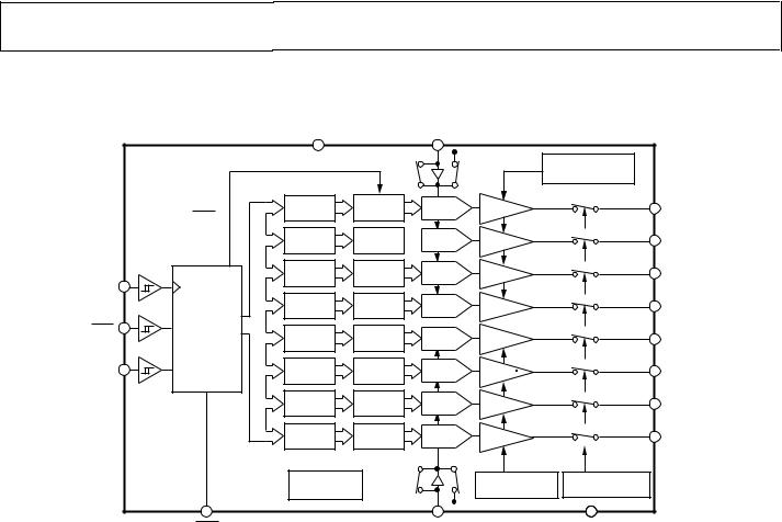
FUNCTIONAL BLOCK DIAGRAM
|
|
VDD |
|
VREFABCD |
|
|
|
|
|
|
VDD |
|
GAIN-SELECT |
|
|
|
|
|
|
|
|
|
|
|
|
|
LOGIC |
|
|
INPUT |
DAC |
STRING |
BUFFER |
VOUTA |
|
LDAC |
REGISTER |
REGISTER |
BUFFER |
||
|
DAC A |
|
|
|||
|
|
INPUT |
STRING |
STRING |
|
|
|
|
DAC |
BUFFER |
VOUTB |
||
|
|
REGISTER |
REGISTER |
DAC B |
||
|
|
|
|
|||
|
|
INPUT |
DAC |
STRING |
BUFFER |
VOUTC |
|
|
REGISTER |
REGISTER |
DAC C |
||
SCLK |
|
|
|
|||
|
|
|
|
|
|
|
|
|
INPUT |
DAC |
STRING |
BUFFER |
VOUTD |
|
INTERFACE |
REGISTER |
REGISTER |
DAC D |
||
|
|
|
||||
SYNC |
|
|
|
|
|
|
LOGIC |
INPUT |
DAC |
STRING |
BUFFER |
VOUTE |
|
|
|
|||||
|
|
REGISTER |
REGISTER |
DAC E |
||
DIN |
|
INPUT |
DAC |
STRING |
BUFFER |
VOUTF |
|
REGISTER |
REGISTER |
DAC F |
|||
|
|
INPUT |
DAC |
STRING |
BUFFER |
VOUTG |
|
|
REGISTER |
REGISTER |
DAC G |
||
|
|
RESET |
DAC |
STRING |
|
|
|
|
INPUT |
BUFFER |
VOUTH |
||
|
|
REGISTER |
REGISTER |
DD |
||
|
|
DAC H |
GND |
|
||
|
|
|
|
|
|
|
|
|
POWER-ON |
|
|
GAIN-SELECT |
POWER-DOWN |
|
|
RESET |
|
|
LOGIC |
LOGIC |
|
|
|
|
VDD |
|
02812001- |
|
LDAC |
|
|
VREFEFGH |
|
GND |
Figure 1.
Rev. F | Page 3 of 28

AD5308/AD5318/AD5328
SPECIFICATIONS
VDD = 2.5 V to 5.5 V; VREF = 2 V; RL = 2 kΩ to GND; CL = 200 pF to GND; all specifications TMIN to TMAX, unless otherwise specified.
Table 1.
|
|
A Version1 |
|
|
B Version1 |
|
|
|
Parameter2 |
Min |
Typ |
Max |
Min |
Typ |
Max |
Unit |
Conditions/Comments |
DC PERFORMANCE3, 4 |
|
|
|
|
|
|
|
|
AD5308 |
|
|
|
|
|
|
|
|
Resolution |
8 |
|
|
8 |
|
|
Bits |
|
Relative Accuracy |
|
±0.15 |
±1 |
|
±0.15 |
±0.75 |
LSB |
|
Differential Nonlinearity |
|
±0.02 |
±0.25 |
|
±0.02 |
±0.25 |
LSB |
Guaranteed monotonic by |
|
|
|
|
|
|
|
|
design over all codes |
AD5318 |
|
|
|
|
|
|
|
|
Resolution |
10 |
|
|
10 |
|
|
Bits |
|
Relative Accuracy |
|
±0.5 |
±4 |
|
±0.5 |
±3 |
LSB |
|
Differential Nonlinearity |
|
±0.05 |
±0.50 |
|
±0.05 |
±0.50 |
LSB |
Guaranteed monotonic by |
|
|
|
|
|
|
|
|
design over all codes |
AD5328 |
|
|
|
|
|
|
|
|
Resolution |
12 |
|
|
12 |
|
|
Bits |
|
Relative Accuracy |
|
±2 |
±16 |
|
±2 |
±12 |
LSB |
|
Differential Nonlinearity |
|
±0.2 |
±1.0 |
|
±0.2 |
±1.0 |
LSB |
Guaranteed monotonic by |
|
|
|
|
|
|
|
|
design over all codes |
Offset Error |
|
±5 |
±60 |
|
±5 |
±60 |
mV |
VDD = 4.5 V, gain = 2, see |
|
|
|
|
|
|
|
|
Figure 27 and Figure 28 |
Gain Error |
|
±0.30 |
±1.25 |
|
±0.30 |
±1.25 |
% of FSR |
VDD = 4.5 V, gain = 2, see |
|
|
|
|
|
|
|
|
Figure 27 and Figure 28 |
Lower Deadband5 |
|
10 |
60 |
|
10 |
60 |
mV |
Lower deadband exists only |
|
|
|
|
|
|
|
|
if offset error is negative, see |
|
|
|
|
|
|
|
|
Figure 27 |
Upper Deadband5 |
|
10 |
60 |
|
10 |
60 |
mV |
Upper deadband exists only |
|
|
|
|
|
|
|
|
if VREF = VDD and offset plus |
|
|
|
|
|
|
|
|
gain error is positive, see |
|
|
|
|
|
|
|
|
Figure 28 |
Offset Error Drift6 |
|
−12 |
|
|
−12 |
|
ppm of |
|
|
|
|
|
|
|
|
FSR/°C |
|
Gain Error Drift6 |
|
−5 |
|
|
−5 |
|
ppm of |
|
|
|
|
|
|
|
|
FSR/°C |
|
DC Power Supply Rejection Ratio6 |
|
−60 |
|
|
−60 |
|
dB |
VDD = ±10% |
DC Crosstalk6 |
|
200 |
|
|
200 |
|
μV |
RL = 2 kΩ to GND or VDD |
DAC REFERENCE INPUTS6 |
|
|
|
|
|
|
|
|
VREF Input Range |
1.0 |
|
VDD |
1.0 |
|
VDD |
V |
Buffered reference mode |
|
0.25 |
|
VDD |
0.25 |
|
VDD |
V |
Unbuffered reference mode |
VREF Input Impedance (RDAC) |
|
>10.0 |
|
|
>10.0 |
|
MΩ |
Buffered reference mode |
|
|
|
|
|
|
|
|
and power-down mode |
|
37.0 |
45.0 |
|
37.0 |
45.0 |
|
kΩ |
Unbuffered reference mode, |
|
|
|
|
|
|
|
|
0 V to VREF output range |
|
18.0 |
22.0 |
|
18.0 |
22.0 |
|
kΩ |
Unbuffered reference mode, |
|
|
|
|
|
|
|
|
0 V to 2 VREF output range |
Reference Feedthrough |
|
−70.0 |
|
|
−70.0 |
|
dB |
Frequency = 10 kHz |
Channel-to-Channel Isolation |
|
−75.0 |
|
|
−75.0 |
|
dB |
Frequency = 10 kHz |
OUTPUT CHARACTERISTICS6 |
|
|
|
|
|
|
|
|
Minimum Output Voltage7 |
|
0.001 |
|
|
0.001 |
|
V |
This is a measure of the |
|
|
|
|
|
|
|
|
minimum and maximum |
Maximum Output Voltage7 |
|
VDD − |
|
|
VDD − 0.001 |
|
V |
Drive capability of the |
|
|
0.001 |
|
|
|
|
|
output amplifier |
DC Output Impedance |
|
0.5 |
|
|
0.5 |
|
Ω |
|
Rev. F | Page 4 of 28

AD5308/AD5318/AD5328
|
|
A Version1 |
|
|
B Version1 |
|
|
|
Parameter2 |
Min |
Typ |
Max |
Min |
Typ |
Max |
Unit |
Conditions/Comments |
Short Circuit Current |
|
25.0 |
|
|
25.0 |
|
mA |
VDD = 5 V |
|
|
16.0 |
|
|
16.0 |
|
mA |
VDD = 3 V |
Power-Up Time |
|
2.5 |
|
|
2.5 |
|
μs |
Coming out of power-down |
|
|
|
|
|
|
|
|
mode, VDD = 5 V |
|
|
5.0 |
|
|
5.0 |
|
μs |
Coming out of power-down |
|
|
|
|
|
|
|
|
mode, VDD = 3 V |
LOGIC INPUTS6 |
|
|
|
|
|
|
|
|
Input Current |
|
|
±1 |
|
|
±1 |
μA |
|
VIL, Input Low Voltage |
|
|
0.8 |
|
|
0.8 |
V |
VDD = 5 V ± 10% |
|
|
|
0.8 |
|
|
0.8 |
V |
VDD = 3 V ± 10% |
|
|
|
0.7 |
|
|
0.7 |
V |
VDD = 2.5 V |
VIH, Input High Voltage |
1.7 |
|
|
1.7 |
|
|
V |
VDD = 2.5 V to 5.5 V, TTL and |
|
|
|
|
|
|
|
|
CMOS compatible |
Pin Capacitance |
|
3.0 |
|
|
3.0 |
|
pF |
|
|
|
|
|
|
|
|
|
|
POWER REQUIREMENTS |
|
|
|
|
|
|
|
|
VDD |
2.5 |
|
5.5 |
2.5 |
|
5.5 |
V |
|
IDD (Normal Mode)8 |
|
|
|
|
|
|
|
VIH = VDD and VIL = GND |
VDD = 4.5 V to 5.5 V |
|
1.0 |
1.8 |
|
1.0 |
1.8 |
mA |
All DACs in unbuffered |
|
|
|
|
|
|
|
|
mode, in buffered mode |
VDD = 2.5 V to 3.6 V |
|
0.7 |
1.5 |
|
0.7 |
1.5 |
mA |
Extra current is typically x μA |
|
|
|
|
|
|
|
|
per DAC; x = (5 μA + |
|
|
|
|
|
|
|
|
VREF/RDAC)/4 |
IDD (Power-Down Mode)9 |
|
|
|
|
|
|
|
VIH = VDD and VIL = GND |
VDD = 4.5 V to 5.5 V |
|
0.4 |
1 |
|
0.4 |
1 |
μA |
|
VDD = 2.5 V to 3.6 V |
|
0.12 |
1 |
|
0.12 |
1 |
μA |
|
|
|
|
|
|
|
|
|
|
1 Temperature range (A, B version): −40°C to +125°C; typical at 25°C. 2 See the Terminology section.
3 DC specifications tested with the outputs unloaded unless stated otherwise.
4 Linearity is tested using a reduced code range: AD5308 (Code 8 to Code 255), AD5318 (Code 28 to Code 1023), and AD5328 (Code 115 to Code 4095). 5 This corresponds to x codes. x = deadband voltage/LSB size.
6 Guaranteed by design and characterization; not production tested.
7For the amplifier output to reach its minimum voltage, offset error must be negative. For the amplifier output to reach its maximum voltage, VREF = VDD and offset plus gain error must be positive.
8 Interface inactive. All DACs active. DAC outputs unloaded.
9 All eight DACs powered down.
VDD = 2.5 V to 5.5 V; RL = 2 kΩ to GND; CL = 200 pF to GND; all specifications TMIN to TMAX, unless otherwise noted.
Table 2. AC Characteristics1
|
|
A, B Version2 |
|
|
|
Parameter3 |
Min |
Typ |
Max |
Unit |
Conditions/Comments |
Output Voltage Settling Time |
|
|
|
|
VREF = VDD = 5 V |
AD5308 |
|
6 |
8 |
μs |
1/4 scale to 3/4 scale change (0x40 to 0xC0) |
AD5318 |
|
7 |
9 |
μs |
1/4 scale to 3/4 scale change (0x100 To 0x300) |
AD5328 |
|
8 |
10 |
μs |
1/4 scale to 3/4 scale change (0x400 to 0xC00) |
Slew Rate |
|
0.7 |
|
V/μs |
|
Major-Code Change Glitch Energy |
|
12 |
|
nV-sec |
1 LSB change around major carry |
Digital Feedthrough |
|
0.5 |
|
nV-sec |
|
Digital Crosstalk |
|
0.5 |
|
nV-sec |
|
Analog Crosstalk |
|
1 |
|
nV-sec |
|
DAC-to-DAC Crosstalk |
|
3 |
|
nV-sec |
|
Multiplying Bandwidth |
|
200 |
|
kHz |
VREF = 2 V ± 0.1 V p-p, unbuffered mode |
Total Harmonic Distortion |
|
−70 |
|
dB |
VREF = 2.5 V ± 0.1 V p-p, frequency = 10 kHz |
|
|
|
|
|
|
1 Guaranteed by design and characterization; not production tested. 2 Temperature range (A, B version): –40°C to +125°C; typical at 25°C. 3 See the Terminology section.
Rev. F | Page 5 of 28
AD5308/AD5318/AD5328
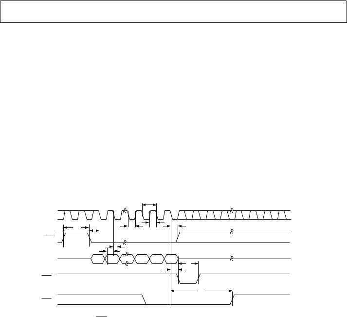
Table 3. Timing Characteristics1, 2, 3
|
A, B Version |
|
|
|
|
|
|
|
|
|
|
|
Parameter |
Limit at TMIN, TMAX |
Unit |
|
Conditions/Comments |
||||||||
|
|
|
|
|
|
|
|
|
|
|
|
|
t1 |
33 |
ns min |
|
SCLK cycle time |
||||||||
t2 |
13 |
ns min |
|
SCLK high time |
||||||||
t3 |
13 |
ns min |
|
SCLK low time |
||||||||
t4 |
13 |
ns min |
|
|
to SCLK falling edge setup time; temperature range (A, B |
|||||||
|
SYNC |
|
||||||||||
|
|
|
|
verstion): −40°C to +105°C |
||||||||
|
15 |
ns min |
|
|
to SCLK falling edge setup time; temperature range (A, B |
|||||||
|
|
SYNC |
|
|||||||||
|
|
|
|
verstion): −40°C to +125°C |
||||||||
t5 |
5 |
ns min |
|
Data set up time |
||||||||
t6 |
4.5 |
ns min |
|
Data hold time |
||||||||
t7 |
0 |
ns min |
|
|
|
|
|
|
rising edge |
|||
|
SCLK falling edge to |
SYNC |
|
|
||||||||
t8 |
50 |
ns min |
|
|
|
|
|
|||||
|
Minimum |
SYNC |
high time |
|||||||||
t9 |
20 |
ns min |
|
|
|
|
||||||
|
LDAC |
pulse width |
||||||||||
t10 |
20 |
ns min |
|
|
rising edge |
|||||||
|
SCLK falling edge to |
LDAC |
|
|||||||||
t11 |
0 |
ns min |
|
|
||||||||
|
SCLK falling edge to |
LDAC |
falling edge |
|||||||||
|
|
|
|
|
|
|
|
|
|
|
|
|
1 Guaranteed by design and characterization; not production tested.
2 All input signals are specified with tR = tF = 5 ns (10% to 90% of VDD) and timed from a voltage level of (VIL + VIH)/2. 3 See Figure 2.
|
|
|
|
t1 |
|
SCLK |
|
|
|
|
|
|
t8 |
|
t3 |
t2 |
t7 |
|
t4 |
|
|||
|
|
|
|
|
|
SYNC |
|
|
|
|
|
|
|
t6 |
t5 |
|
|
DIN |
|
DB15 |
|
|
DB0 |
|
|
|
|
|
t9 |
|
|
|
|
|
t11 |
LDAC1 |
|
|
|
|
|
t10
LDAC2
NOTES
1ASYNCHRONOUS LDAC UPDATE MODE.
2SYNCHRONOUS LDAC UPDATE MODE.
Figure 2. Serial Interface Timing Diagram
02812-002
Rev. F | Page 6 of 28
ABSOLUTE MAXIMUM RATINGS
TA = 25°C, unless otherwise specified.
Table 4.
Parameter |
Rating1 |
VDD to GND |
−0.3 V to +7 V |
Digital Input Voltage to GND |
−0.3 V to VDD + 0.3 V |
Reference Input Voltage to GND |
−0.3 V to VDD + 0.3 V |
VOUTA–VOUTD to GND |
−0.3 V to VDD + 0.3 V |
Operating Temperature Range |
|
Industrial (A, B Version) |
−40°C to +125°C |
Storage Temperature Range |
−65°C to +150°C |
Junction Temperature (TJ MAX) |
150°C |
16-Lead TSSOP |
|
Power Dissipation |
(TJ MAX − TA)/θJA |
θJA Thermal Impedance |
150.4°C/W |
Lead Temperature |
JEDEC industry-standard |
Soldering |
J-STD-020 |
|
|
1 Transient currents of up to 100 mA do not cause SCR latch-up.
AD5308/AD5318/AD5328
Stresses above those listed under Absolute Maximum Ratings may cause permanent damage to the device. This is a stress rating only; functional operation of the device at these or any other conditions above those indicated in the operational section of this specification is not implied. Exposure to absolute maximum rating conditions for extended periods may affect device reliability.
ESD CAUTION
Rev. F | Page 7 of 28

AD5308/AD5318/AD5328
PIN CONFIGURATION AND FUNCTION DESCRIPTIONS
|
LDAC |
|
|
1 |
|
16 |
SCLK |
|
|
|
|
2 |
|
15 |
DIN |
||
SYNC |
|
|||||||
|
VDD |
3 |
AD5308/ |
14 |
GND |
|||
VOUTA |
4 |
AD5318/ |
13 |
VOUTH |
||||
AD5328 |
||||||||
VOUTB |
5 |
12 |
VOUTG |
|||||
TOP VIEW |
||||||||
VOUTC |
6 |
11 |
VOUTF |
|||||
(Not to Scale) |
||||||||
VOUTD |
7 |
|
10 |
VOUTE |
||||
V ABCD |
8 |
|
9 |
V EFGH |
||||
REF |
|
|
|
REF |
||||
Figure 3. Pin Configuration
02812-003
Table 5. Pin Function Descriptions
Pin No. |
|
Mnemonic |
Description |
||||
1 |
|
|
|
|
This active low control input transfers the contents of the input registers to their respective DAC registers. Pulsing |
||
|
LDAC |
|
|||||
|
|
|
|
|
this pin low allows any or all DAC registers to be updated if the input registers have new data. This allows simul- |
||
|
|
|
|
|
taneous updates of all DAC outputs. Alternatively, this pin can be tied permanently low. |
||
2 |
|
|
Active Low Control Input. This is the frame synchronization signal for the input data. When |
|
goes low, it |
||
|
SYNC |
|
SYNC |
||||
|
|
|
|
|
powers on the SCLK and DIN buffers and enables the input shift register. Data is transferred in on the falling edges |
||
|
|
|
|
|
of the following 16 clocks. If SYNC is taken high before the 16th falling edge, the rising edge of SYNC acts as an |
||
|
|
|
|
|
interrupt and the write sequence is ignored by the device. |
||
3 |
|
VDD |
Power Supply Input. These parts can be operated from 2.5 V to 5.5 V, and the supply should be decoupled with a 10 μF |
||||
|
|
|
|
|
capacitor in parallel with a 0.1 μF capacitor to GND. |
||
4 |
|
VOUTA |
Buffered Analog Output Voltage from DAC A. The output amplifier has rail-to-rail operation. |
||||
5 |
|
VOUTB |
Buffered Analog Output Voltage from DAC B. The output amplifier has rail-to-rail operation. |
||||
6 |
|
VOUTC |
Buffered Analog Output Voltage from DAC C. The output amplifier has rail-to-rail operation. |
||||
7 |
|
VOUTD |
Buffered Analog Output Voltage from DAC D. The output amplifier has rail-to-rail operation. |
||||
8 |
|
VREFABCD |
Reference Input Pin for DACs A, B, C, and D. It can be configured as a buffered, unbuffered, or VDD input to the four |
||||
|
|
|
|
|
DACs, depending on the state of the BUF and VDD control bits. It has an input range from 0.25 V to VDD in unbuffered |
||
|
|
|
|
|
mode and from 1 V to VDD in buffered mode. |
||
9 |
|
VREFEFGH |
Reference Input Pin for DACs E, F, G, and H. It can be configured as a buffered, unbuffered, or VDD input to the four |
||||
|
|
|
|
|
DACs, depending on the state of the BUF and VDD control bits. It has an input range from 0.25 V to VDD in unbuffered |
||
|
|
|
|
|
mode and from 1 V to VDD in buffered mode. |
||
10 |
|
VOUTE |
Buffered Analog Output Voltage from DAC E. The output amplifier has rail-to-rail operation. |
||||
11 |
|
VOUTF |
Buffered Analog Output Voltage from DAC F. The output amplifier has rail-to-rail operation. |
||||
12 |
|
VOUTG |
Buffered Analog Output Voltage from DAC G. The output amplifier has rail-to-rail operation. |
||||
13 |
|
VOUTH |
Buffered Analog Output Voltage from DAC H. The output amplifier has rail-to-rail operation. |
||||
14 |
|
GND |
Ground Reference Point for All Circuitry on the Part. |
||||
15 |
|
DIN |
Serial Data Input. This device has a 16-bit shift register. Data is clocked into the register on the falling edge of the |
||||
|
|
|
|
|
serial clock input. The DIN input buffer is powered down after each write cycle. |
||
16 |
|
SCLK |
Serial Clock Input. Data is clocked into the input shift register on the falling edge of the serial clock input. Data can |
||||
|
|
|
|
|
be transferred at rates up to 30 MHz. The SCLK input buffer is powered down after each write cycle. |
||
Rev. F | Page 8 of 28

TYPICAL PERFORMANCE CHARACTERISTICS
|
1.0 |
|
|
|
|
|
|
|
TA = 25°C |
|
|
|
|
|
|
VDD = 5V |
|
|
|
|
|
0.5 |
|
|
|
|
|
(LSB) |
|
|
|
|
|
|
INL ERROR |
0 |
|
|
|
|
|
|
|
|
|
|
|
|
|
–0.5 |
|
|
|
|
|
|
–1.0 |
50 |
100 |
150 |
200 |
250 |
|
0 |
|||||
|
|
|
|
CODE |
|
02812006- |
Figure 4. AD5308 Typical INL Plot
|
3 |
|
|
|
|
|
|
|
TA = 25°C |
|
|
|
|
|
2 |
VDD = 5V |
|
|
|
|
|
|
|
|
|
|
|
(LSB) |
1 |
|
|
|
|
|
|
|
|
|
|
|
|
INL ERROR |
0 |
|
|
|
|
|
–1 |
|
|
|
|
|
|
|
|
|
|
|
|
|
|
–2 |
|
|
|
|
02812-007 |
|
–3 |
|
|
|
|
|
|
200 |
400 |
600 |
800 |
1000 |
|
|
0 |
|||||
|
|
|
|
CODE |
|
|
Figure 5. AD5318 Typical INL Plot
|
12 |
|
|
|
|
|
|
|
|
|
|
TA = 25°C |
|
|
|
|
|
|
|
|
8 |
VDD = 5V |
|
|
|
|
|
|
|
|
|
|
|
|
|
|
|
|
|
(LSB) |
4 |
|
|
|
|
|
|
|
|
|
|
|
|
|
|
|
|
|
|
INL ERROR |
0 |
|
|
|
|
|
|
|
|
–4 |
|
|
|
|
|
|
|
|
|
|
|
|
|
|
|
|
|
|
|
|
–8 |
|
|
|
|
|
|
|
02812-008 |
|
–12 |
|
|
|
|
|
|
|
|
|
500 |
1000 |
1500 |
2000 |
2500 |
3000 |
3500 |
4000 |
|
|
0 |
||||||||
|
|
|
|
|
CODE |
|
|
|
|
Figure 6. AD5328 Typical INL Plot
|
|
|
AD5308/AD5318/AD5328 |
|||
|
0.3 |
TA = 25°C |
|
|
|
|
|
|
|
|
|
|
|
|
|
VDD = 5V |
|
|
|
|
|
0.2 |
|
|
|
|
|
(LSB) |
0.1 |
|
|
|
|
|
|
|
|
|
|
|
|
DNL ERROR |
0 |
|
|
|
|
|
–0.1 |
|
|
|
|
|
|
|
–0.2 |
|
|
|
|
02812-009 |
|
–0.3 |
|
|
|
|
|
|
50 |
100 |
150 |
200 |
250 |
|
|
0 |
|||||
|
|
|
|
CODE |
|
|
Figure 7. AD5308 Typical DNL Plot
|
0.6 |
|
|
|
|
|
|
|
|
|
|
TA = 25°C |
|
|
|
|
|
|
|
|
0.4 |
VDD = 5V |
|
|
|
|
|
|
|
|
|
|
|
|
|
|
|
|
|
(LSB) |
0.2 |
|
|
|
|
|
|
|
|
|
|
|
|
|
|
|
|
|
|
ERRORDNL |
–0.2 |
|
|
|
|
|
|
|
|
|
0 |
|
|
|
|
|
|
|
|
|
–0.4 |
|
|
|
|
|
|
|
02812-010 |
|
–0.6 |
|
|
|
|
|
|
|
|
|
200 |
400 |
|
600 |
800 |
|
1000 |
||
|
0 |
|
|
||||||
|
|
|
|
|
CODE |
|
|
|
|
|
|
Figure 8. AD5318 Typical DNL Plot |
|
|
|||||
|
1.0 |
|
|
|
|
|
|
|
|
|
|
TA = 25°C |
|
|
|
|
|
|
|
|
|
VDD = 5V |
|
|
|
|
|
|
|
|
0.5 |
|
|
|
|
|
|
|
|
(LSB) |
|
|
|
|
|
|
|
|
|
ERRORDNL |
0 |
|
|
|
|
|
|
|
|
|
|
|
|
|
|
|
|
|
|
|
–0.5 |
|
|
|
|
|
|
|
|
|
–1.0 |
|
|
|
|
|
|
|
02812-011 |
|
500 |
1000 |
1500 |
2000 |
2500 |
3000 |
3500 |
4000 |
|
|
0 |
||||||||
CODE
Figure 9. AD5328 Typical DNL Plot
Rev. F | Page 9 of 28
Loading...