


 Loading...
|
2.7 V to 5.5 V, <100 μA, 8-/10-/12-Bit |
|
nanoDAC, SPI Interface in LFCSP and SC70 |
Data Sheet |
AD5601/AD5611/AD5621 |
|
|
FEATURES
6-lead SC70 and LFCSP packages
Micropower operation: 100 µA maximum at 5 V Power-down typically to 0.2 µA at 3 V
2.7 V to 5.5 V power supply Guaranteed monotonic by design
Power-on reset to 0 V with brownout detection 3 power-down functions
Low power serial interface with Schmitt-triggered inputs On-chip output buffer amplifier, rail-to-rail operation SYNC interrupt facility
Minimized zero-code error AD5601 buffered 8-bit DAC B version: ±0.5 LSB INL AD5611 buffered 10-bit DAC B version: ±0.5 LSB INL
A version: ±4 LSB INL AD5621 buffered 12-bit DAC
B version: ±1 LSB INL A version: ±6 LSB INL
APPLICATIONS
Voltage level setting
Portable battery-powered instruments
Digital gain and offset adjustment
Programmable voltage and current sources
Programmable attenuators
GENERAL DESCRIPTION
The AD5601/AD5611/AD5621, members of the nanoDAC® family, are single, 8-/10-/12-bit, buffered voltage output DACs that operate from a single 2.7 V to 5.5 V supply, consuming typically 75 µA at 5 V. The parts come in tiny LFCSP and SC70 packages. Their on-chip precision output amplifier allows rail- to-rail output swing to be achieved. The AD5601/AD5611/ AD5621 utilize a versatile 3-wire serial interface that operates at clock rates up to 30 MHz and is compatible with SPI, QSPI™, MICROWIRE™, and DSP interface standards.
The reference for the AD5601/AD5611/AD5621 is derived from the power supply inputs and, therefore, gives the widest dynamic output range. The parts incorporate a power-on reset circuit, which ensures that the DAC output powers up to 0 V and remains there until a valid write to the device takes place.
The AD5601/AD5611/AD5621 contain a power-down feature that reduces current consumption to typically 0.2 µA at 3 V.
Rev. F
Information furnished by Analog Devices is believed to be accurate and reliable. However, no responsibilityisassumedbyAnalogDevicesforitsuse,norforanyinfringementsofpatentsorother rightsofthirdpartiesthatmayresultfromitsuse.Specificationssubjecttochangewithoutnotice.No license is granted by implication or otherwise under any patent or patent rights of Analog Devices. Trademarksandregisteredtrademarksarethepropertyoftheirrespectiveowners.
FUNCTIONAL BLOCK DIAGRAM
|
VDD |
GND |
|
|
|
POWER-ON |
|
|
AD5601/AD5611/AD5621 |
||
RESET |
|
|
|
|
|
DAC |
REF(+) |
OUTPUT |
VOUT |
||
12-/10-/8-BIT |
|||||
REGISTER |
BUFFER |
||||
DAC |
|
||||
|
|
|
|||
INPUT |
|
POWER-DOWN |
|
||
CONTROL |
|
RESISTOR |
|||
|
CONTROL LOGIC |
||||
LOGIC |
|
|
|
NETWORK |
|
|
|
|
|
06853-001 |
|
SYNC SCLK SDIN
|
Figure 1. |
Table 1. Related Devices |
|
Part Number |
Description |
AD5641 |
2.7 V to 5.5 V, <100 µA, 14-bit nanoDAC in |
|
SC70 and LFCSP packages |
|
|
They also provide software-selectable output loads while in power-down mode. The parts are put into power-down mode over the serial interface.
The low power consumption of these parts in normal operation makes them ideally suited to portable battery-operated equipment. The combination of small package and low power makes these nanoDAC devices ideal for level-setting requirements, such as generating bias or control voltages in space-constrained and power-sensitive applications.
PRODUCT HIGHLIGHTS
1.Available in 6-lead LFCSP and SC70 packages.
2.Low power, single-supply operation. The AD5601/ AD5611/AD5621 operate from a single 2.7 V to 5.5 V supply with a maximum current consumption of 100 µA, making them ideal for battery-powered applications.
3.The on-chip output buffer amplifier allows the output of the DAC to swing rail-to-rail with a typical slew rate of 0.5 V/µs.
4.Reference is derived from the power supply.
5.High speed serial interface with clock speeds up to 30 MHz. Designed for very low power consumption. The interface powers up only during a write cycle.
6.Power-down capability. When powered down, the DAC typically consumes 0.2 µA at 3 V. Power-on reset with brownout detection.
One Technology Way, P.O. Box 9106, Norwood, MA 02062-9106, U.S.A. Tel: 781.329.4700 www.analog.com Fax: 781.461.3113 ©2005–2012 Analog Devices, Inc. All rights reserved.

AD5601/AD5611/AD5621 |
Data Sheet |
TABLE OF CONTENTS |
|
Features .............................................................................................. |
1 |
Applications....................................................................................... |
1 |
General Description ......................................................................... |
1 |
Functional Block Diagram .............................................................. |
1 |
Product Highlights ........................................................................... |
1 |
Revision History ............................................................................... |
2 |
Specifications..................................................................................... |
3 |
Timing Characteristics ................................................................ |
4 |
Absolute Maximum Ratings............................................................ |
5 |
ESD Caution.................................................................................. |
5 |
Pin Configuration and Function Descriptions............................. |
6 |
Typical Performance Characteristics ............................................. |
7 |
Terminology .................................................................................... |
13 |
Theory of Operation ...................................................................... |
14 |
DAC Section................................................................................ |
14 |
Resistor String............................................................................. |
14 |
REVISION HISTORY |
|
2/12—Rev. E to Rev. F |
|
Added 6-Lead LFCSP......................................................... |
Universal |
Changes to Features Section, General Description Section, |
|
Table 1, and Product Highlights Section ....................................... |
1 |
Changes to Table 4............................................................................ |
5 |
Added Figure 4; Renumbered Sequentially .................................. |
6 |
Changes to Table 5............................................................................ |
6 |
Changes to Choosing a Reference as Power Supply for the |
|
AD5601/AD5611/AD5621 Section.............................................. |
18 |
Updated Outline Dimensions ....................................................... |
20 |
Changes to Ordering Guide .......................................................... |
21 |
7/10—Rev. D to Rev. E |
|
Changes to Figure 1.......................................................................... |
1 |
5/08—Rev. C to Rev. D |
|
Changes to General Description Section ...................................... |
1 |
Changes to Table 2............................................................................ |
3 |
Changes to Choosing a Reference as Power Supply for the |
|
AD5601/AD5611/AD5621 Section.............................................. |
18 |
Changes to Ordering Guide .......................................................... |
20 |
Output Amplifier........................................................................ |
14 |
Serial Interface ............................................................................ |
14 |
Input Shift Register .................................................................... |
14 |
SYNC Interrupt .......................................................................... |
14 |
Power-On Reset.......................................................................... |
16 |
Power-Down Modes .................................................................. |
16 |
Microprocessor Interfacing....................................................... |
16 |
Applications..................................................................................... |
18 |
Choosing a Reference as Power Supply for the |
|
AD5601/AD5611/AD5621 ....................................................... |
18 |
Bipolar Operation Using the AD5601/AD5611/AD5621..... |
18 |
Using the AD5601/AD5611/AD5621 with a Galvanically |
|
Isolated Interface ........................................................................ |
19 |
Power Supply Bypassing and Grounding................................ |
19 |
Outline Dimensions ....................................................................... |
20 |
Ordering Guide .......................................................................... |
21 |
12/07—Rev. B to Rev. C |
|
Changes to Features .......................................................................... |
1 |
Changes to Table 2............................................................................. |
3 |
Changes to AD5601/AD5611/AD5621 to ADSP-2101 |
|
Interface Section ............................................................................. |
16 |
Updated Outline Dimensions....................................................... |
20 |
Changes to Ordering Guide .......................................................... |
20 |
7/05—Rev. A to Rev. B |
|
Changes to Figure 48...................................................................... |
17 |
Changes to Galvanically Isolated Interface Section................... |
19 |
Changes to Figure 52...................................................................... |
19 |
3/05—Rev. 0 to Rev. A |
|
Changes to Timing Characteristics................................................. |
4 |
Changes to Absolute Maximum Ratings........................................ |
5 |
Changes to Full Scale Error Section................................................ |
7 |
Changes to Figure 20...................................................................... |
10 |
Changes to Theory of Operation.................................................. |
14 |
Changes to Power Down Modes .................................................. |
15 |
1/05—Revision 0: Initial Version |
|
Rev. F | Page 2 of 24

Data Sheet |
AD5601/AD5611/AD5621 |
SPECIFICATIONS
VDD = 2.7 V to 5.5 V; RL = 2 kΩ to GND; CL = 200 pF to GND; all specifications TMIN to TMAX, unless otherwise noted. Temperature range for A/B grades is −40°C to +125°C, typical at 25°C.
Table 2.
|
A Grade |
|
B Grade |
|
|
|
Parameter |
Min Typ |
Max |
Min Typ |
Max |
Unit |
Test Conditions/Comments |
STATIC PERFORMANCE |
|
|
|
|
|
|
AD5601 |
|
|
|
|
|
|
Resolution |
|
|
8 |
|
Bits |
|
Relative Accuracy1 (INL) |
|
|
|
±0.5 |
LSB |
|
Differential Nonlinearity (DNL) |
|
|
|
±0.5 |
LSB |
Guaranteed monotonic by design |
AD5611 |
|
|
|
|
|
|
Resolution |
10 |
|
|
|
Bits |
|
Relative Accuracy1 (INL) |
|
±4 |
|
±0.5 |
LSB |
|
Differential Nonlinearity (DNL) |
|
±0.5 |
|
±0.5 |
LSB |
Guaranteed monotonic by design |
AD5621 |
|
|
|
|
|
|
Resolution |
12 |
|
|
|
Bits |
|
Relative Accuracy1 (INL) |
|
±6 |
|
±1 |
LSB |
|
Differential Nonlinearity (DNL) |
|
±0.5 |
|
±0.5 |
LSB |
Guaranteed monotonic by design |
Zero-Code Error |
0.5 |
10 |
0.5 |
10 |
mV |
All 0s loaded to DAC register |
Full-Scale Error |
±0.5 |
|
±0.5 |
|
mV |
All 1s loaded to DAC register |
Offset Error |
±0.063 |
±10 |
±0.063 |
±10 |
mV |
|
Gain Error |
±0.0004 |
±0.037 |
±0.0004 |
±0.037 |
%FSR |
|
Zero-Code Error Drift |
5.0 |
|
5.0 |
|
µV/°C |
|
Gain Temperature Coefficient |
2.0 |
|
2.0 |
|
ppm |
|
|
|
|
|
|
FSR/°C |
|
|
|
|
|
|
|
|
OUTPUT CHARACTERISTICS2 |
|
|
|
|
|
|
Output Voltage Range |
0 |
VDD |
0 |
VDD |
V |
|
Output Voltage Settling Time |
6 |
10 |
6 |
10 |
µs |
Code ¼ scale to ¾ scale |
Slew Rate |
0.5 |
|
0.5 |
|
V/µs |
|
Capacitive Load Stability |
470 |
|
470 |
|
pF |
RL = ∞ |
|
1000 |
|
1000 |
|
pF |
RL = 2 kΩ |
Output Noise Spectral Density |
120 |
|
120 |
|
nV/√Hz |
DAC code = midscale,1 kHz |
Noise |
2 |
|
2 |
|
µV |
DAC code = midscale, |
|
|
|
|
|
|
0.1 Hz to 10 kHz bandwidth |
Digital-to-Analog Glitch Impulse |
5 |
|
5 |
|
nV-s |
1 LSB change around major carry |
Digital Feedthrough |
0.2 |
|
0.2 |
|
nV-s |
|
Short-Circuit Current |
15 |
|
15 |
|
mA |
VDD = 3 V/5 V |
DC Output Impedance |
0.5 |
|
0.5 |
|
Ω |
|
LOGIC INPUTS |
|
|
|
|
|
|
Input Current3 |
|
±2 |
|
±2 |
µA |
|
Input High Voltage, VINH |
1.8 |
|
1.8 |
|
V |
VDD = 4.7 V to 5.5 V |
|
1.4 |
|
1.4 |
|
V |
VDD = 2.7 V to 3.6 V |
Input Low Voltage, VINL |
|
0.8 |
|
0.8 |
V |
VDD = 4.7 V to 5.5 V |
|
|
0.6 |
|
0.6 |
V |
VDD = 2.7 V to 3.6 V |
Pin Input Capacitance |
3 |
|
3 |
|
pF |
|
|
|
|
|
|
|
|
Rev. F | Page 3 of 24
AD5601/AD5611/AD5621 |
|
|
|
|
|
Data Sheet |
|
|
|
|
|
|
|
|
|
|
|
|
|
|
|
|
|
|
|
A Grade |
|
B Grade |
|
|
|
Parameter |
Min |
Typ |
Max |
Min Typ |
Max |
Unit |
Test Conditions/Comments |
|
|
|
|
|
|
|
|
POWER REQUIREMENTS |
|
|
|
|
|
|
|
VDD |
2.7 |
|
5.5 |
2.7 |
5.5 |
V |
All digital inputs at 0 V or VDD |
IDD for Normal Mode |
|
|
|
|
|
|
DAC active and excluding load |
|
|
|
|
|
|
|
current |
VDD = ±4.5 V to ±5.5 V |
|
75 |
100 |
75 |
100 |
µA |
VIH = VDD and VIL = GND |
VDD = ±2.7 V to ±3.6 V |
|
60 |
90 |
60 |
90 |
µA |
VIH = VDD and VIL = GND |
IDD for All Power-Down Modes |
|
|
|
|
|
|
VIH = VDD and VIL = GND |
VDD = ±4.5 V to ±5.5 V |
|
0.5 |
|
0.5 |
|
µA |
VIH = VDD and VIL = GND |
VDD = ±2.7 V to ±3.6 V |
|
0.2 |
|
0.2 |
|
µA |
VIH = VDD and VIL = GND |
|
|
|
|
|
|
|
|
POWER EFFICIENCY |
|
|
|
|
|
|
|
IOUT/IDD |
|
96 |
|
96 |
|
% |
ILOAD = 2 mA and VDD = ±5 V |
1Linearity calculated using a reduced code range: AD5621 from Code 64 to Code 4032; AD5611 from Code 16 to Code 1008; AD5601 from Code 4 to Code 252.
2Guaranteed by design and characterization, not production tested.
3Total current flowing into all pins.
TIMING CHARACTERISTICS
VDD = 2.7 V to 5.5 V; all specifications TMIN to TMAX, unless otherwise noted. See Figure 2.
Table 3.
Parameter |
Limit1 |
Unit |
|
Test Conditions/Comments |
|||||
t12 |
33 |
ns min |
|
SCLK cycle time |
|||||
t2 |
5 |
ns min |
|
SCLK high time |
|||||
t3 |
5 |
ns min |
|
SCLK low time |
|||||
t4 |
10 |
ns min |
|
|
|
|
|
|
|
|
SYNC |
to SCLK falling edge setup time |
|||||||
t5 |
5 |
ns min |
|
Data setup time |
|||||
t6 |
4.5 |
ns min |
|
Data hold time |
|||||
|
|
|
|
|
|
|
|||
t7 |
0 |
ns min |
|
SCLK falling edge to |
SYNC |
rising edge |
|||
|
|
|
|
|
|||||
t8 |
20 |
ns min |
|
Minimum |
SYNC |
high time |
|||
t9 |
13 |
ns min |
|
|
|||||
|
SYNC |
rising edge to next SCLK falling edge ignored |
|||||||
|
|
|
|
|
|
|
|
|
|
1All input signals are specified with tr = tf = 1 ns/V (10% to 90% of VDD) and timed from a voltage level of (VIL + VIH)/2.
2Maximum SCLK frequency is 30 MHz.
t4 |
t2 |
t1 |
t9 |
SCLK |
|
|
|
t8 |
t3 |
|
t7 |
SYNC |
|
|
|
|
|
|
t6 |

 t5
t5 
SDIN |
D15 |
D14 |
D2 |
D1 |
D0 |
D15 |
D14 |
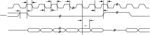
Figure 2. Timing Diagram
06853-002
Rev. F | Page 4 of 24
Data Sheet |
AD5601/AD5611/AD5621 |
ABSOLUTE MAXIMUM RATINGS
TA = 25°C, unless otherwise noted.
Table 4.
Parameter |
Rating |
|
|
VDD to GND |
−0.3 V to +7.0 V |
Digital Input Voltage to GND |
−0.3 V to VDD + 0.3 V |
VOUT to GND |
−0.3 V to VDD + 0.3 V |
Operating Temperature Range |
|
Industrial (A/B Grades) |
−40°C to +125°C |
Storage Temperature Range |
−65°C to +160°C |
Maximum Junction Temperature |
150°C |
SC70 Package |
|
θJA Thermal Impedance |
433.34°C/W |
θJC Thermal Impedance |
149.47°C/W |
LFCSP Package |
|
θJA Thermal Impedance |
95°C/W |
Lead Temperature, Soldering |
|
Vapor Phase (60 sec) |
215°C |
Infrared (15 sec) |
220°C |
ESD (Human Body Model) |
2.0 kV |
Stresses above those listed under Absolute Maximum Ratings may cause permanent damage to the device. This is a stress rating only; functional operation of the device at these or any other conditions above those indicated in the operational section of this specification is not implied. Exposure to absolute maximum rating conditions for extended periods may affect device reliability.
ESD CAUTION
Rev. F | Page 5 of 24
AD5601/AD5611/AD5621
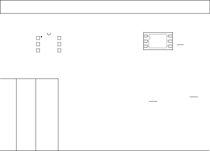
PIN CONFIGURATION AND FUNCTION DESCRIPTIONS
|
|
|
1 |
|
|
|
6 |
VOUT |
|
|
|
|
AD5601/ |
|
|||||
SYNC |
|
||||||||
SCLK |
2 |
AD5611/ |
5 |
GND |
|
||||
AD5621 |
-003 |
||||||||
|
SDIN |
3 |
TOP VIEW |
4 |
VDD |
||||
|
|
|
|
(Not to Scale) |
|
|
06853 |
||
|
|
|
|
|
|
|
|
|
|
Figure 3. 6-Lead SC70 Pin Configuration
Data Sheet
VDD |
1 |
AD5601/ |
6 |
VOUT |
|
SCLK |
2 |
AD5611/ |
5 |
GND |
|
AD5621 |
|
||||
SDIN |
3 |
TOP VIEW |
4 |
SYNC |
|
(Not to Scale) |
|
||||
NOTES: |
|
|
|
-053 |
|
|
|
|
06853 |
||
1. CONNECT THE EXPOSED PAD TO GND. |
|||||
Figure 4. 6-Lead LFCSP Pin Configuration
Table 5. Pin Function Descriptions
SC70 |
LFCSP |
|
|
Pin No. |
Pin No. |
Mnemonic |
|
1 |
4 |
|
|
SYNC |
|
||
2 |
2 |
SCLK |
3 |
3 |
SDIN |
4 |
1 |
VDD |
5 |
5 |
GND |
6 |
6 |
VOUT |
|
|
EP |
Description
Level-Triggered Control Input (Active Low). This is the frame synchronization signal for the input data. When SYNC goes low, it enables the input shift register, and data is transferred in on the falling edges of the clocks that follow. The DAC is updated following the 16th clock cycle, unless SYNC is taken high before this edge, in which case the rising edge of SYNC acts as an interrupt and the write sequence is ignored by the DAC.
Serial Clock Input. Data is clocked into the input shift register on the falling edge of the serial clock input. Data can be transferred at rates up to 30 MHz.
Serial Data Input. This device has a 16-bit shift register. Data is clocked into the register on the falling edge of the serial clock input.
Power Supply Input. The AD5601/AD5611/AD5621 can be operated from 2.7 V to 5.5 V. VDD should be decoupled to GND.
Ground. Ground reference point for all circuitry on the AD5601/AD5611/AD5621. Analog Output Voltage from the DAC. The output amplifier has rail-to-rail operation. Exposed Pad. Connect to GND.
Rev. F | Page 6 of 24
Data Sheet
TYPICAL PERFORMANCE CHARACTERISTICS
1.0VDD = VREF = 5V TA = 25°C
(LSB) |
0.5 |
|
|
|
|
|
|
|
|
|
|
|
|
|
|
|
|
|
|
|
|
|
|
|
|
|
|
|
|
|
|
|
|
|
|
|
|
|
|
|
|
|
|
|
|
|
|
|
|
|
|
|
|
|
|
|
|
|
|
|
|
|
|
||
|
|
|
|
|
|
|
|
|
|
|
|
|
|
|
|
|
|
|
|
|
|
|
|
|
|
|
|
|
|
|
|
|
ERRORINL |
0 |
|
|
|
|
|
|
|
|
|
|
|
|
|
|
|
|
|
|
|
|
|
|
|
|
|
|
|
|
|
|
|
|
|
|
|
|
|
|
|
|
|
|
|
|
|
|
|
|
|
|
|
|
|
|
|
|
|
|
|
|
|
|
|
|
|
–0.5 |
|
|
|
|
|
|
|
|
|
|
|
|
|
|
|
|
|
|
|
|
|
|
|
|
|
|
|
|
|
|
|
|
|
|
|
|
|
|
|
|
|
|
|
|
|
|
|
|
|
|
|
|
|
|
|
|
|
|
|
|
|
|
|
|
|
–1.0 |
|
|
|
|
|
|
|
|
|
|
|
|
|
|
|
|
|
|
|
|
|
|
|
|
|
|
|
|
|
|
-004 |
|
|
|
|
|
|
|
|
|
|
|
|
|
|
|
|
|
|
|
|
|
|
|
|
|
|
|
|
|
|
|
||
|
64 |
|
564 |
1064 |
|
|
|
1564 |
|
2064 |
2564 |
3064 3564 |
|
4064 |
||||||||||||||||||
|
|
|
|
|
|
|
|
|
|
|
|
|
|
|
|
|
DAC CODE |
|
|
|
|
|
|
|
|
|
06853 |
|||||
|
|
|
|
|
|
|
|
|
|
Figure 5. Typical AD5621 INL |
|
|
|
|
|
|
|
|
||||||||||||||
|
0.5 |
|
|
|
|
|
|
|
|
|
|
|
|
|
|
|
|
|
|
|
|
|
|
|
|
|
|
|
|
|
|
|
|
|
|
|
VDD = VREF = 5V |
|
|
|
|
|
|
|
|
|
|
|
|
|
|
|
|
|
|
|
|
||||||||
|
|
|
|
|
|
|
|
|
|
|
|
|
|
|
|
|
|
|
|
|
|
|
|
|
||||||||
|
0.4 |
|
|
|
TA = 25°C |
|
|
|
|
|
|
|
|
|
|
|
|
|
|
|
|
|
|
|
|
|
||||||
|
|
|
|
|
|
|
|
|
|
|
|
|
|
|
|
|
|
|
|
|
|
|
|
|
||||||||
|
0.3 |
|
|
|
|
|
|
|
|
|
|
|
|
|
|
|
|
|
|
|
|
|
|
|
|
|
|
|
|
|
|
|
|
|
|
|
|
|
|
|
|
|
|
|
|
|
|
|
|
|
|
|
|
|
|
|
|
|
|
|
|
|
|
|
|
|
|
|
|
|
|
|
|
|
|
|
|
|
|
|
|
|
|
|
|
|
|
|
|
|
|
|
|
|
|
|
|
|
(LSB) |
0.2 |
|
|
|
|
|
|
|
|
|
|
|
|
|
|
|
|
|
|
|
|
|
|
|
|
|
|
|
|
|
|
|
|
|
|
|
|
|
|
|
|
|
|
|
|
|
|
|
|
|
|
|
|
|
|
|
|
|
|
|
|
|
|
||
0.1 |
|
|
|
|
|
|
|
|
|
|
|
|
|
|
|
|
|
|
|
|
|
|
|
|
|
|
|
|
|
|
|
|
ERROR |
|
|
|
|
|
|
|
|
|
|
|
|
|
|
|
|
|
|
|
|
|
|
|
|
|
|
|
|
|
|
|
|
0 |
|
|
|
|
|
|
|
|
|
|
|
|
|
|
|
|
|
|
|
|
|
|
|
|
|
|
|
|
|
|
|
|
|
|
|
|
|
|
|
|
|
|
|
|
|
|
|
|
|
|
|
|
|
|
|
|
|
|
|
|
|
|
|
|
|
INL |
–0.1 |
|
|
|
|
|
|
|
|
|
|
|
|
|
|
|
|
|
|
|
|
|
|
|
|
|
|
|
|
|
|
|
|
|
|
|
|
|
|
|
|
|
|
|
|
|
|
|
|
|
|
|
|
|
|
|
|
|
|
|
|
|
|||
–0.2 |
|
|
|
|
|
|
|
|
|
|
|
|
|
|
|
|
|
|
|
|
|
|
|
|
|
|
|
|
|
|
||
|
|
|
|
|
|
|
|
|
|
|
|
|
|
|
|
|
|
|
|
|
|
|
|
|
|
|
|
|
|
|
||
|
|
|
|
|
|
|
|
|
|
|
|
|
|
|
|
|
|
|
|
|
|
|
|
|
|
|
|
|
|
|
||
|
–0.3 |
|
|
|
|
|
|
|
|
|
|
|
|
|
|
|
|
|
|
|
|
|
|
|
|
|
|
|
|
|
|
|
|
|
|
|
|
|
|
|
|
|
|
|
|
|
|
|
|
|
|
|
|
|
|
|
|
|
|
|
|
|
|
||
|
–0.4 |
|
|
|
|
|
|
|
|
|
|
|
|
|
|
|
|
|
|
|
|
|
|
|
|
|
|
|
|
|
|
|
|
|
|
|
|
|
|
|
|
|
|
|
|
|
|
|
|
|
|
|
|
|
|
|
|
|
|
|
|
|
|
||
|
–0.5 |
|
|
|
|
|
|
|
|
|
|
|
|
|
|
|
|
|
|
|
|
|
|
|
|
|
|
|
|
|
||
|
|
|
|
|
|
|
|
|
|
|
|
|
|
|
|
|
|
|
|
|
|
|
|
|
|
|
005- |
|||||
|
16 |
116 |
216 |
|
316 |
416 |
516 |
616 |
716 |
816 |
916 |
|||||||||||||||||||||
|
|
06853 |
||||||||||||||||||||||||||||||
|
|
|
|
|
|
|
|
|
|
|
|
|
|
|
|
|
DAC CODE |
|
|
|
|
|
|
|
||||||||
|
|
|
|
|
|
|
|
|
|
Figure 6. Typical AD5611 INL |
|
|
|
|
|
|
|
|
||||||||||||||
|
0.100 |
|
|
|
|
|
|
|
|
|
|
|
|
|
|
|
|
|
|
|
|
|
||||||||||
|
|
|
VDD = VREF = 5V |
|
|
|
|
|
|
|
|
|
|
|
|
|
|
|
|
|
|
|||||||||||
|
0.075 |
|
|
TA = 25°C |
|
|
|
|
|
|
|
|
|
|
|
|
|
|
|
|
|
|
|
|
|
|||||||
|
|
|
|
|
|
|
|
|
|
|
|
|
|
|
|
|
|
|
|
|
|
|
||||||||||
|
|
|
|
|
|
|
|
|
|
|
|
|
|
|
|
|
|
|
|
|
|
|
|
|
|
|
|
|
|
|||
|
|
|
|
|
|
|
|
|
|
|
|
|
|
|
|
|
|
|
|
|
|
|
|
|
|
|
|
|
|
|||
|
0.050 |
|
|
|
|
|
|
|
|
|
|
|
|
|
|
|
|
|
|
|
|
|
|
|
|
|
|
|
|
|
||
|
|
|
|
|
|
|
|
|
|
|
|
|
|
|
|
|
|
|
|
|
|
|
|
|
|
|
|
|
|
|||
(LSB) |
0.025 |
|
|
|
|
|
|
|
|
|
|
|
|
|
|
|
|
|
|
|
|
|
|
|
|
|
|
|
|
|
||
|
|
|
|
|
|
|
|
|
|
|
|
|
|
|
|
|
|
|
|
|
|
|
|
|
|
|
|
|
||||
ERROR |
0 |
|
|
|
|
|
|
|
|
|
|
|
|
|
|
|
|
|
|
|
|
|
|
|
|
|
|
|
|
|
||
INL |
|
|
|
|
|
|
|
|
|
|
|
|
|
|
|
|
|
|
|
|
|
|
|
|
|
|
|
|
|
|||
–0.025 |
|
|
|
|
|
|
|
|
|
|
|
|
|
|
|
|
|
|
|
|
|
|
|
|
|
|
|
|
||||
|
|
|
|
|
|
|
|
|
|
|
|
|
|
|
|
|
|
|
|
|
|
|
|
|
|
|
|
|||||
|
|
|
|
|
|
|
|
|
|
|
|
|
|
|
|
|
|
|
|
|
|
|
|
|
|
|
|
|
|
|
|
|
|
–0.050 |
|
|
|
|
|
|
|
|
|
|
|
|
|
|
|
|
|
|
|
|
|
|
|
|
|
|
|
|
|||
|
|
|
|
|
|
|
|
|
|
|
|
|
|
|
|
|
|
|
|
|
|
|
|
|
|
|
|
|
||||
|
–0.075 |
|
|
|
|
|
|
|
|
|
|
|
|
|
|
|
|
|
|
|
|
|
|
|
|
|
|
|
|
|||
|
|
|
|
|
|
|
|
|
|
|
|
|
|
|
|
|
|
|
|
|
|
|
|
|
|
|
|
|
||||
|
–0.100 4 |
|
|
|
|
|
|
|
|
|
|
|
|
|
|
|
|
|
|
|
|
|
|
|
-006 |
|||||||
|
54 |
|
|
|
|
104 |
|
154 |
|
|
204 |
|
|
|
|
|||||||||||||||||
|
|
|
|
|
|
|
|
|
|
|
|
|
|
|
|
|
|
DAC CODE |
|
|
|
|
|
|
|
|
|
06853 |
||||
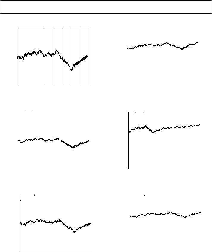
Figure 7. Typical AD5601 INL
AD5601/AD5611/AD5621
|
|
2.5 |
|
|
|
|
|
|
|
|
|
|
|
|
|
|
|
|
|
|
|
|
|
|
|
|
|
|
|
|
|
|
|
|
|
|
|
|
VDD = VREF = 5V |
|
|
|
|
|
|
|
|
|
|
|
|
|
|
|
|
|
|
|
|
|
|
|
|
|
|||||||
|
|
|
|
|
|
|
|
|
|
|
|
|
|
|
|
|
|
|
|
|
|
|
|
|
|
|
|
|
|||||||
(LSB) |
|
2.0 |
|
TA = 25°C |
|
|
|
|
|
|
|
|
|
|
|
|
|
|
|
|
|
|
|
|
|
|
|
|
|
|
|
|
|||
|
|
|
|
|
|
|
|
|
|
|
|
|
|
|
|
|
|
|
|
|
|
|
|
|
|
|
|
|
|||||||
|
1.5 |
|
|
|
|
|
|
|
|
|
|
|
|
|
|
|
|
|
|
|
|
|
|
|
|
|
|
|
|
|
|
|
|
|
|
ERROR |
|
|
|
|
|
|
|
|
|
|
|
|
|
|
|
|
|
|
|
|
|
|
|
|
|
|
|
|
|
|
|
|
|
|
|
|
1.0 |
|
|
|
|
|
|
|
|
|
|
|
|
|
|
|
|
|
|
|
|
|
|
|
|
|
|
|
|
|
|
|
|
|
|
|
|
|
|
|
|
|
|
|
|
|
|
|
|
|
|
|
|
|
|
|
|
|
|
|
|
|
|
|
|
|
|
|
|
|
|
UNADJUSTED |
|
0.5 |
|
|
|
|
|
|
|
|
|
|
|
|
|
|
|
|
|
|
|
|
|
|
|
|
|
|
|
|
|
|
|
|
|
|
|
|
|
|
|
|
|
|
|
|
|
|
|
|
|
|
|
|
|
|
|
|
|
|
|
|
|
|
|
|
|
|
|
||
|
0 |
|
|
|
|
|
|
|
|
|
|
|
|
|
|
|
|
|
|
|
|
|
|
|
|
|
|
|
|
|
|
|
|
|
|
|
|
|
|
|
|
|
|
|
|
|
|
|
|
|
|
|
|
|
|
|
|
|
|
|
|
|
|
|
|
|
|
|
|
|
|
|
–0.5 |
|
|
|
|
|
|
|
|
|
|
|
|
|
|
|
|
|
|
|
|
|
|
|
|
|
|
|
|
|
|
|
|
|
|
|
|
|
|
|
|
|
|
|
|
|
|
|
|
|
|
|
|
|
|
|
|
|
|
|
|
|
|
|
|
|
|
|
|
||
TOTAL |
–1.0 |
|
|
|
|
|
|
|
|
|
|
|
|
|
|
|
|
|
|
|
|
|
|
|
|
|
|
|
|
|
|
|
|
|
|
|
|
|
|
|
|
|
|
|
|
|
|
|
|
|
|
|
|
|
|
|
|
|
|
|
|
|
|
|
|
|
|
|
|||
–1.5 |
|
|
|
|
|
|
|
|
|
|
|
|
|
|
|
|
|
|
|
|
|
|
|
|
|
|
|
|
|
|
|
|
|
||
|
|
|
|
|
|
|
|
|
|
|
|
|
|
|
|
|
|
|
|
|
|
|
|
|
|
|
|
|
|
|
|
|
|
||
|
–2.0 |
|
|
|
|
|
|
|
|
|
|
|
|
|
|
|
|
|
|
|
|
|
|
|
|
|
|
|
|
|
|
|
|
|
|
|
|
|
|
|
|
|
|
|
|
|
|
|
|
|
|
|
|
|
|
|
|
|
|
|
|
|
|
|
|
|
|
|
|
||
|
–2.5 |
|
|
|
|
|
|
|
|
|
|
|
|
|
|
|
|
|
|
|
|
|
|
|
|
|
|
|
|
|
|
|
|
-007 |
|
|
|
|
|
|
|
|
|
|
|
|
|
|
|
|
|
|
|
|
|
|
|
|
|
|
|
|
|
|
4064 |
||||||
|
|
64 |
|
|
564 |
1064 |
1564 |
|
2064 |
2564 |
3064 |
3564 |
|
||||||||||||||||||||||
|
|
|
|
|
|
06853 |
|||||||||||||||||||||||||||||
|
|
|
|
|
|
|
|
|
|
|
|
|
|
|
DAC CODE |
|
|
|
|
|
|
|
|
|
|
|
|
|
|
|
|||||
|
|
|
|
|
|
Figure 8. AD5621 Total Unadjusted Error (TUE) |
|
|
|
|
|
||||||||||||||||||||||||
|
|
0.6 |
|
|
|
|
|
|
|
|
|
|
|
|
|
|
|
|
|
|
|
|
|
|
|
|
|
|
|
|
|
|
|
|
|
|
|
|
|
VDD = VREF = 5V |
|
|
|
|
|
|
|
|
|
|
|
|
|
|
|
|
|
|
|
|
|
|
|
|
|||||||
|
|
|
|
|
|
|
|
|
|
|
|
|
|
|
|
|
|
|
|
|
|
|
|
|
|
|
|
||||||||
(LSB) |
|
|
|
TA = 25°C |
|
|
|
|
|
|
|
|
|
|
|
|
|
|
|
|
|
|
|
|
|
|
|
|
|
||||||
0.4 |
|
|
|
|
|
|
|
|
|
|
|
|
|
|
|
|
|
|
|
|
|
|
|
|
|
|
|
|
|
|
|
|
|
||
|
|
|
|
|
|
|
|
|
|
|
|
|
|
|
|
|
|
|
|
|
|
|
|
|
|
|
|
|
|
|
|
|
|||
|
|
|
|
|
|
|
|
|
|
|
|
|
|
|
|
|
|
|
|
|
|
|
|
|
|
|
|
|
|
|
|
|
|
||
ERROR |
0.2 |
|
|
|
|
|
|
|
|
|
|
|
|
|
|
|
|
|
|
|
|
|
|
|
|
|
|
|
|
|
|
|
|
|
|
UNADJUSTEDTOTAL |
–0.4 |
|
|
|
|
|
|
|
|
|
|
|
|
|
|
|
|
|
|
|
|
|
|
|
|
|
|
|
|
|
|
|
|
|
|
|
|
0 |
|
|
|
|
|
|
|
|
|
|
|
|
|
|
|
|
|
|
|
|
|
|
|
|
|
|
|
|
|
|
|
|
|
|
|
–0.2 |
|
|
|
|
|
|
|
|
|
|
|
|
|
|
|
|
|
|
|
|
|
|
|
|
|
|
|
|
|
|
|
-008 |
|
|
|
|
|
|
|
|
|
|
|
|
|
|
|
|
|
|
|
|
|
|
|
|
|
|
|
|
|
|
|||||||
|
|
–0.616 |
|
|
|
|
|
|
|
|
|
|
|
|
|
|
|
|
|
|
|
|
|
|
|
|
|
|
|
||||||
|
|
116 |
216 |
|
316 416 |
516 |
616 |
716 |
|
816 916 |
|
||||||||||||||||||||||||
|
|
|
|
|
|
|
|
|
|
|
|
|
|
|
|
DAC CODE |
|
|
|
|
|
|
|
|
06853 |
||||||||||
|
|
|
|
|
|
Figure 9. AD5611 Total Unadjusted Error (TUE) |
|
|
|
|
|
||||||||||||||||||||||||
|
|
0.20 |
|
|
|
|
|
|
|
|
|
|
|
|
|
|
|
|
|
|
|
|
|
|
|
|
|
|
|
|
|
|
|
||
|
|
|
|
|
|
VDD = VREF = 5V |
|
|
|
|
|
|
|
|
|
|
|
|
|
|
|
|
|
|
|
|
|||||||||
(LSB) |
0.15 |
|
TA = 25°C |
|
|
|
|
|
|
|
|
|
|
|
|
|
|
|
|
|
|
|
|
|
|
|
|
|
|||||||
|
|
|
|
|
|
|
|
|
|
|
|
|
|
|
|
|
|
|
|
|
|
|
|
|
|
|
|
|
|
|
|||||
0.10 |
|
|
|
|
|
|
|
|
|
|
|
|
|
|
|
|
|
|
|
|
|
|
|
|
|
|
|
|
|
|
|
||||
ERROR |
|
|
|
|
|
|
|
|
|
|
|
|
|
|
|
|
|
|
|
|
|
|
|
|
|
|
|
|
|
|
|
||||
0.05 |
|
|
|
|
|
|
|
|
|
|
|
|
|
|
|
|
|
|
|
|
|
|
|
|
|
|
|
|
|
|
|
||||
UNADJUSTED |
|
|
|
|
|
|
|
|
|
|
|
|
|
|
|
|
|
|
|
|
|
|
|
|
|
|
|
|
|
|
|
||||
|
0 |
|
|
|
|
|
|
|
|
|
|
|
|
|
|
|
|
|
|
|
|
|
|
|
|
|
|
|
|
|
|
|
|||
|
|
|
|
|
|
|
|
|
|
|
|
|
|
|
|
|
|
|
|
|
|
|
|
|
|
|
|
|
|
|
|
|
|
||
TOTAL |
–0.05 |
|
|
|
|
|
|
|
|
|
|
|
|
|
|
|
|
|
|
|
|
|
|
|
|
|
|
|
|
|
|
|
|||
|
|
|
|
|
|
|
|
|
|
|
|
|
|
|
|
|
|
|
|
|
|
|
|
|
|
|
|
|
|
|
|||||
–0.10 |
|
|
|
|
|
|
|
|
|
|
|
|
|
|
|
|
|
|
|
|
|
|
|
|
|
|
|
|
|
|
|
||||
|
|
|
|
|
|
|
|
|
|
|
|
|
|
|
|
|
|
|
|
|
|
|
|
|
|
|
|
|
|
|
|
|
|||
|
|
–0.15 |
|
|
|
|
|
|
|
|
|
|
|
|
|
|
|
|
|
|
|
|
|
|
|
|
|
|
|
|
|
|
009- |
||
|
|
|
|
|
|
|
|
|
|
|
|
|
|
|
|
|
|
|
|
|
|
|
|
|
|
|
|
|
|
|
|
||||
|
|
–0.20 |
|
|
|
|
|
|
|
|
|
|
|
|
|
|
|
|
|
|
|
|
|
|
|
|
|
|
|
|
|
|
|||
|
|
|
|
|
54 |
104 |
|
|
154 |
|
|
|
204 |
|
|
|
|
|
|
||||||||||||||||
|
|
|
4 |
|
|
|
|
|
|
|
|
|
|
|
|
|
06853 |
||||||||||||||||||
|
|
|
|
|
|
|
|
|
|
|
|
|
|
|
|
|
DAC CODE |
|
|
|
|
|
|
|
|
|
|
|
|
||||||
Figure 10. AD5601 Total Unadjusted Error (TUE)
Rev. F | Page 7 of 24

AD5601/AD5611/AD5621 |
|
|
|
|||||||
|
0.20 |
|
VDD = 5V |
|
|
|
|
|
|
|
|
|
|
|
|
|
|
|
|
|
|
|
0.15 |
|
TA = 25°C |
|
|
|
|
|
|
|
|
|
|
|
|
|
|
|
|
|
|
(LSB)ERRORDNL |
0.10 |
|
|
|
|
|
|
|
|
DEVICESOFNUMBER |
0.05 |
|
|
|
|
|
|
|
|
||
|
|
|
|
|
|
|
|
|
|
|
|
0 |
0 |
|
|
|
|
|
|
|
|
|
–0.05 |
|
|
|
|
|
|
|
|
|
|
–0.10 |
|
|
|
|
|
|
|
|
|
|
–0.15 |
|
|
|
|
|
|
|
|
|
|
–0.20 |
64 |
564 |
1064 |
1564 |
2064 |
2564 |
3064 |
3564 |
-010 |
|
|
06853 |
||||||||
|
|
|
|
|
DAC CODE |
|
|
|
||
Data Sheet
12 |
|
|
|
|
|
|
|
|
|
|
|
|
|
|
|
|
|
|
|
|
|
|
|
|
|
|
|
|
|
|
|
|
|
|
|
|
|
|
|
|
|
|
|
VDD = 3V |
|
|
|
|
|
|
|
|
|
|
|
|
|
|
|
|
|
|
|
|
|
|
|
|
VDD = 5V |
|
|||||||||||||||
|
|
|
|
|
|
|
|
|
|
|
|
|
|
|
|
|
|
|
|
|
|
|
|
|
|
|
||||||||||||||||
|
|
VIH |
|
= DVDD |
|
|
|
|
|
|
|
|
|
|
|
|
|
|
|
|
|
|
|
|
|
|
|
|
VIH |
= DVDD |
|
|||||||||||
|
|
V |
= GND |
|
|
|
|
|
|
|
|
|
|
|
|
|
|
|
|
|
|
|
|
|
|
|
|
V |
= GND |
|
||||||||||||
10 |
|
TAIL |
= 25°C |
|
|
|
|
|
|
|
|
|
|
|
|
|
|
|
|
|
|
|
|
|
|
|
|
TAIL |
= 25°C |
|
||||||||||||
|
|
|
|
|
|
|
|
|
|
|
|
|
|
|
|
|
|
|
|
|
|
|
||||||||||||||||||||
8 |
|
|
|
|
|
|
|
|
|
|
|
|
|
|
|
|
|
|
|
|
|
|
|
|
|
|
|
|
|
|
|
|
|
|
|
|
|
|
|
|
|
|
|
|
|
|
|
|
|
|
|
|
|
|
|
|
|
|
|
|
|
|
|
|
|
|
|
|
|
|
|
|
|
|
|
|
|
|
|
|
|
|
|
|
|
|
|
|
|
|
|
|
|
|
|
|
|
|
|
|
|
|
|
|
|
|
|
|
|
|
|
|
|
|
|
|
|
|
|
|
|
|
|
|
|
|
|
|
6 |
|
|
|
|
|
|
|
|
|
|
|
|
|
|
|
|
|
|
|
|
|
|
|
|
|
|
|
|
|
|
|
|
|
|
|
|
|
|
|
|
|
|
|
|
|
|
|
|
|
|
|
|
|
|
|
|
|
|
|
|
|
|
|
|
|
|
|
|
|
|
|
|
|
|
|
|
|
|
|
|
|
|
|
|
|
|
|
|
|
|
|
|
|
|
|
|
|
|
|
|
|
|
|
|
|
|
|
|
|
|
|
|
|
|
|
|
|
|
|
|
|
|
|
|
|
|
|
|
4 |
|
|
|
|
|
|
|
|
|
|
|
|
|
|
|
|
|
|
|
|
|
|
|
|
|
|
|
|
|
|
|
|
|
|
|
|
|
|
|
|
|
|
|
|
|
|
|
|
|
|
|
|
|
|
|
|
|
|
|
|
|
|
|
|
|
|
|
|
|
|
|
|
|
|
|
|
|
|
|
|
|
|
|
|
|
|
|
|
|
|
|
|
|
|
|
|
|
|
|
|
|
|
|
|
|
|
|
|
|
|
|
|
|
|
|
|
|
|
|
|
|
|
|
|
|
|
|
|
2 |
|
|
|
|
|
|
|
|
|
|
|
|
|
|
|
|
|
|
|
|
|
|
|
|
|
|
|
|
|
|
|
|
|
|
|
|
|
|
|
|
|
|
|
|
|
|
|
|
|
|
|
|
|
|
|
|
|
|
|
|
|
|
|
|
|
|
|
|
|
|
|
|
|
|
|
|
|
|
|
|
|
|
|
|
|
0 |
|
|
|
|
|
|
|
|
|
|
|
|
|
|
|
|
|
|
|
|
|
|
|
|
|
|
|
|
|
|
|
|
|
|
|
|
|
|
|
|
|
|
|
|
|
|
|
|
|
|
|
|
|
|
|
|
|
|
|
|
|
|
|
|
|
|
|
|
|
|
|
|
|
|
|
|
|
|
|
|
|
|
|
|
|
|
|
|
|
|
|
|
0.06710 |
0.06773 0.06835 0.06897 0.06960 0.07022 0.07084 0.07147 0.07209 0.07271 0.07334 06853-013 |
0.05456 0.05527 |
0.05599 |
0.05671 |
0.05742 |
0.05814 |
I |
0.05885 |
(mA)0.06648 |
|
|
|
|
|
|
|
DD |
|
|
Figure 11. Typical AD5621 DNL |
Figure 14. IDD Histogram (3 V/5 V) |
|
0.05 |
VDD = 5V |
|
|
|
|
|
|
|
|
|
|
|
|
|
|
|
|
|
|
|
|
|
|
0.04 |
TA = 25°C |
|
|
|
|
|
|
|
|
|
|
0.03 |
|
|
|
|
|
|
|
|
|
|
(LSB) |
0.02 |
|
|
|
|
|
|
|
|
|
|
0.01 |
|
|
|
|
|
|
|
|
|
|
|
ERROR |
0 |
|
|
|
|
|
|
|
|
|
|
–0.01 |
|
|
|
|
|
|
|
|
|
|
|
DNL |
|
|
|
|
|
|
|
|
|
|
|
–0.02 |
|
|
|
|
|
|
|
|
|
|
|
|
|
|
|
|
|
|
|
|
|
|
|
|
–0.03 |
|
|
|
|
|
|
|
|
|
|
|
–0.04 |
|
|
|
|
|
|
|
|
|
|
|
–0.05 |
|
|
|
|
|
|
|
|
|
011- |
|
16 |
116 |
216 |
316 |
416 |
516 |
616 |
716 |
816 |
916 |
06853 |
|
|
|
|
|
DAC CODE |
|
|
|
|||
Figure 12. Typical AD5611 DNL
|
0.010 |
VDD = 5V |
|
|
|
|
|
0.008 |
|
|
|
|
|
|
TA = 25°C |
|
|
|
|
|
|
0.006 |
|
|
|
|
|
(LSB) |
0.004 |
|
|
|
|
|
0.002 |
|
|
|
|
|
|
|
|
|
|
|
|
|
ERROR |
0 |
|
|
|
|
|
–0.002 |
|
|
|
|
|
|
DNL |
|
|
|
|
|
|
–0.004 |
|
|
|
|
|
|
|
|
|
|
|
|
|
|
–0.006 |
|
|
|
|
|
|
–0.008 |
|
|
|
|
|
|
–0.010 |
|
|
|
|
-012 |
|
4 |
54 |
104 |
154 |
204 |
|
|
06853 |
|||||
|
|
|
DAC CODE |
|
||
|
|
|
|
|
||
Figure 13. Typical AD5601 DNL
TA = 25°C
VDD = 5V
CH1 = SCLK
|
|
|
|
|
|
|
|
|
|
|
|
|
|
|
|
|
|
|
|
|
|
|
|
|
|
|
|
|
|
|
|
|
|
|
|
|
|
|
|
|
|
|
|
|
|
|
|
|
|
|
|
|
|
|
|
|
|
|
CH2 = VOUT |
|
||
|
|
|
|
|
|
|
|
06853-014 |
|
|
|
|
|
|
|
|
|
|
CH1 = 5V/DIV CH2 = 1V/DIV TIME BASE = 2µs/DIV |
|||||||
Figure 15. Full-Scale Settling Time
|
|
TA = 25°C |
|
|
VDD = 5V |
|
CH1 = SCLK |
|
|
CH2 = VOUT |
|
|
|
06853-015 |
CH1 = 5V/DIV |
CH2 = 1V/DIV |
TIME BASE = 2µs/DIV |
Figure 16. Half-Scale Settling Time
Rev. F | Page 8 of 24
Loading...