


 Loading...
a |
2-Channel, 256-Position |
|
Digital Potentiometer |
||
|
|
|
|
|
AD5207 |
|
|
|
FEATURES 256-Position, 2-Channel
Potentiometer Replacement 10 k , 50 k , 100 k
Power Shut-Down, Less than 5 A
2.7 V to 5.5 V Single Supply2.7 V Dual Supply
3-Wire SPI-Compatible Serial Data Input Midscale Preset During Power-On
APPLICATIONS
Mechanical Potentiometer Replacement
Stereo Channel Audio Level Control
Instrumentation: Gain, Offset Adjustment
Programmable Voltage-to-Current Conversion
Programmable Filters, Delays, Time Constants
Line Impedance Matching
Automotive Electronics Adjustment
FUNCTIONAL BLOCK DIAGRAM
A1 |
W1 |
B1 |
A2 |
W2 |
B2 |
|
SHDN |
|
|
|
|
|
|
RDAC1 REGISTER |
RDAC2 REGISTER |
|||||
VDD |
|
R |
|
|
R |
|
|
|
|
|
|||
VSS |
|
|
|
|
|
|
LOGIC |
|
|
|
POWER- |
||
CS |
|
|
|
|
ON |
|
|
AD5207 |
8 |
|
RESET |
||
|
|
|
||||
CLK |
SERIAL INPUT REGISTER |
SDO |
||||
SDI |
||||||
|
|
|
|
|
||
DGND |
|
|
|
|
|
|
GENERAL DESCRIPTION
The AD5207 provides dual channel, 256-position, digitally controlled variable resistor (VR) devices that perform the same electronic adjustment function as a potentiometer or variable resistor. Each channel of the AD5207 contains a fixed resistor with a wiper contact that taps the fixed resistor value at a point determined by a digital code loaded into the SPI-compatible serial-input register. The resistance between the wiper and either end point of the fixed resistor varies linearly with respect to the digital code transferred into the VR latch. The variable resistor offers a completely programmable value of resistance, between the A Terminal and the wiper or the B Terminal and the wiper. The fixed A-to-B terminal resistance of 10 kΩ, 50 kΩ or 100 kΩ has a ± 1% channel-to-channel matching tolerance with a nominal temperature coefficient of 500 ppm/°C. A unique switching circuit minimizes the high glitch inherent in traditional switched resistor designs and avoids any make-before-break or break- before-make operation.
Each VR has its own VR latch, which holds its programmed resistance value. These VR latches are updated from an internal serial-to-parallel shift register, which is loaded from a standard 3-wire serial-input digital interface. Ten bits, to make up the data word, are required and clocked into the serial input register.
REV. 0
Information furnished by Analog Devices is believed to be accurate and reliable. However, no responsibility is assumed by Analog Devices for its use, nor for any infringements of patents or other rights of third parties that may result from its use. No license is granted by implication or otherwise under any patent or patent rights of Analog Devices.
The first two bits are address bits. The following eight bits are the data bits that represent the 256 steps of the resistance value. The reason for two address bits instead of one is to be compatible with similar products such as AD8402 so that drop-in replacement is possible. The address bit determines the corresponding VR latch to be loaded with the data bits during the returned positive edge of CS strobe. A serial data output pin at the opposite end of the serial register allows simple daisy chaining in multiple VR applications without additional external decoding logic.
An internal reset block will force the wiper to the midscale position during every power-up condition. The SHDN pin forces an open circuit on the A Terminal and at the same time shorts the wiper to the B Terminal, achieving a microwatt power shutdown state. When SHDN is returned to logic high, the previous latch settings put the wiper in the same resistance setting prior to shutdown. The digital interface remains active during shutdown; code changes can be made to produce new wiper positions when the device is resumed from shutdown.
The AD5207 is available in 1.1 mm thin TSSOP-14 package, which is suitable for PCMCIA applications. All parts are guaranteed to operate over the extended industrial temperature range of –40°C to +125°C.
One Technology Way, P.O. Box 9106, Norwood, MA 02062-9106, U.S.A.
Tel: 781/329-4700 |
www.analog.com |
Fax: 781/326-8703 |
© Analog Devices, Inc., 2001 |
AD5207–SPECIFICATIONS
ELECTRICAL CHARACTERISTICS 10 k , 50 k , 100 k VERSION (VDD = 5 V, VSS = 0, VA = 5 V,
VB = 0, –40 C < TA < +125 C unless otherwise noted.)
Parameter |
Symbol |
Conditions |
Min |
Typ1 |
Max |
Unit |
DC CHARACTERISTICS |
|
|
|
|
|
|
RHEOSTAT MODE |
|
|
|
|
|
|
Specifications Apply to All VRs |
|
|
|
|
|
|
Resistor Differential Nonlinearity2 |
R-DNL |
RWB, VA = NC |
–1 |
|
+1 |
LSB |
Resistor Nonlinearity2 |
R-INL |
RWB, VA = NC |
–1.5 |
|
+1.5 |
LSB |
Nominal Resistor Tolerance3 |
∆R |
|
–30 |
|
+30 |
% |
Resistance Temperature Coefficient |
RAB/∆T |
VAB = VDD, Wiper = No Connect |
|
500 |
|
ppm/°C |
Wiper Resistance |
RW |
IW = 1 V/R, VDD = 5 V |
|
50 |
100 |
Ω |
Nominal Resistance Match |
∆R/RO |
Ch 1 to 2, VAB = VDD, TA = 25°C |
|
0.2 |
1 |
% |
DC CHARACTERISTICS |
|
|
|
|
|
|
POTENTIOMETER DIVIDER MODE |
|
|
|
|
|
|
Specifications Apply to All VRs |
|
|
|
|
|
|
Resolution |
N |
|
8 |
|
|
Bits |
Integral Nonlinearity4 |
INL |
|
–1.5 |
|
+1.5 |
LSB |
Differential Nonlinearity4 |
DNL |
VDD = 5 V, VSS = 0 V |
–1 |
|
+1 |
LSB |
Voltage Divider Temperature |
∆VW/∆T |
Code = 80H |
|
15 |
|
ppm/°C |
Coefficient |
|
|
|
|
|
|
Full-Scale Error |
VWFSE |
Code = FFH |
–1.5 |
|
|
LSB |
Zero-Scale Error |
VWZSE |
Code = 00H |
|
|
+1.5 |
LSB |
RESISTOR TERMINALS |
|
|
|
|
|
|
Voltage Range5 |
VA, B, W |
|VDD| + |VSS| ≤5.5 V |
VSS |
|
VDD |
V |
Capacitance6 AX, BX |
CA,B |
f = 1 MHz, Measured to GND, Code = 80H |
|
45 |
|
pF |
Capacitance6 WX |
CW |
f = 1 MHz, Measured to GND, Code = 80H |
|
70 |
|
pF |
Shutdown Current7 |
IA_SD |
VA = VDD, VB = 0 V, SHDN = 0 |
|
|
5 |
µA |
Shutdown Wiper Resistance |
RW_SD |
VA = VDD, VB = 0 V, SHDN = 0, VDD = 5 V |
|
|
200 |
Ω |
Common-Mode Leakage |
ICM |
VA = VB = VDD/2 |
|
1 |
|
nA |
DIGITAL INPUTS AND OUTPUTS |
|
|
|
|
|
|
Input Logic High |
VIH |
VDD = 5 V, VSS = 0 V |
2.4 |
|
|
V |
Input Logic Low |
VIL |
VDD = 5 V, VSS = 0 V |
|
|
0.8 |
V |
Input Logic High |
VIH |
VDD = 3 V, VSS = 0 V |
2.1 |
|
|
V |
Input Logic Low |
VIL |
VDD = 3 V, VSS = 0 V |
|
|
0.6 |
V |
Output Logic High |
VOH |
RL = 1 kΩ to VDD |
VDD – 0.1 |
|
|
V |
Output Logic Low |
VOL |
IOL = 1.6 mA, VDD = 5 V |
|
|
0.4 |
V |
Input Current |
IIL |
VIN = 0 V or 5 V |
|
|
±10 |
µA |
Input Capacitance6 |
CIL |
|
|
10 |
|
pF |
POWER SUPPLIES |
|
|
|
|
|
|
Power Single-Supply Range |
VDD RANGE |
VSS = 0 V |
2.7 |
|
5.5 |
V |
Power Dual-Supply Range |
VDD/SS RANGE |
|
±2.2 |
|
±2.7 |
V |
Positive Supply Current |
IDD |
VIH = VDD or VIL = GND, VSS = 0 V |
|
|
40 |
µA |
Negative Supply Current |
ISS |
VIH = VDD or VIL = GND VSS = –2.5 V |
|
|
40 |
µA |
Power Dissipation8 |
PDISS |
VIH = 5 V or VIL = 0 V, VDD = 5 V |
|
|
0.2 |
mW |
Power Supply Sensitivity, VDD |
PSS |
∆VDD = 5 V ± 10%, VSS = 0 V, Code = 80H |
|
|
0.01 |
%/% |
Power Supply Sensitivity, VSS |
PSS |
∆VSS = –2.5 V ± 10%, VDD = 2.5 V, Code = 80H |
|
|
0.03 |
%/% |
DYNAMIC CHARACTERISTICS6, 9 |
|
|
|
|
|
|
Bandwidth –3 dB |
BW_10 kΩ |
RAB = 10 kΩ |
|
600 |
|
kHz |
Bandwidth –3 dB |
BW_50 kΩ |
RAB = 50 kΩ |
|
125 |
|
kHz |
Bandwidth –3 dB |
BW_100 kΩ |
RAB = 100 kΩ |
|
71 |
|
kHz |
Total Harmonic Distortion |
THDW |
VA = 1 V rms, VB = 0 V, f = 1 kHz, RAB = 10 kΩ |
|
0.003 |
|
% |
VW Settling Time |
tS |
RAB = 10 kΩ/50 kΩ/100 kΩ, ±1 LSB Error Band |
|
2/9/18 |
|
µs |
Resistor Noise Voltage |
eN_WB |
RWB = 5 kΩ, f = 1 kHz, RS = 0 |
|
9 |
|
nV√Hz |
Crosstalk10 |
CT |
VA = 5 V, VB = 0 V |
|
–65 |
|
dB |
–2– |
REV. 0 |
|
|
|
|
|
|
AD5207 |
|
|
|
|
|
|
|
|
|
Parameter |
Symbol |
Conditions |
Min |
Typ1 |
Max |
|
Unit |
INTERFACE TIMING |
|
|
|
|
|
|
|
CHARACTERISTICS |
|
|
|
|
|
|
|
Applies to All Parts6, 11 |
|
|
|
|
|
|
|
Input Clock Pulsewidth |
tCH, tCL |
Clock Level High or Low |
10 |
|
|
|
ns |
Data Setup Time |
tDS |
|
5 |
|
|
|
ns |
Data Hold Time |
tDH |
RL = 1 kΩ to 5 V, CL < 20 pF |
5 |
|
|
|
ns |
CLK to SDO Propagation Delay12 |
tPD |
1 |
|
25 |
|
ns |
|
CS Setup Time |
tCSS |
|
10 |
|
|
|
ns |
CS High Pulsewidth |
tCSW |
|
10 |
|
|
|
ns |
CLK Fall to CS Fall Hold Time |
tCSH0 |
|
0 |
|
|
|
ns |
CLK Fall to CS Rise Hold Time |
tCSH1 |
|
0 |
|
|
|
ns |
CS Rise to Clock Rise Setup |
tCS1 |
|
10 |
|
|
|
ns |
NOTES
1Typicals represent average readings at 25°C and VDD = 5 V, VSS = 0 V.
2Resistor position nonlinearity error R-INL is the deviation from an ideal value measured between the maximum resistance and the minimum resistance wiper positions. R-DNL measures the relative step change from ideal between successive tap positions. Parts are guaranteed monotonic. I W = VDD/R for both VDD = 5 V, VSS = 0 V.
3VAB = VDD, Wiper (VW) = No connect.
4INL and DNL are measured at VW with the RDAC configured as a potentiometer divider similar to a voltage output D/A converter. V A = VDD and VB = 0 V. DNL specification limits of ±1 LSB maximum are Guaranteed Monotonic operating conditions.
5Resistor Terminals A, B, W have no limitations on polarity with respect to each other.
6Guaranteed by design and not subject to production test.
7Measured at the AX terminals. All AX terminals are open-circuited in shut-down mode.
8PDISS is calculated from (IDD × VDD). CMOS logic level inputs result in minimum power dissipation.
9All dynamic characteristics use VDD = 5 V, VSS = 0 V.
10Measured at a VW pin where an adjacent VW pin is making a full-scale voltage change.
11 See timing diagram for location of measured values. All input control voltages are specified with t R = tF = 2 ns (10% to 90% of 3 V) and timed from a voltage level of 1.5 V. Switching characteristics are measured using VDD = 5 V.
12 Propagation delay depends on value of VDD, RL, and CL; see applications text.
The AD5207 contains 474 transistors. Die Size: 67 mil × 69 mil, 4623 sq. mil. Specifications subject to change without notice.
|
1 |
|
|
|
|
|
|
|
|
|
SDI |
A1 |
A0 |
D7 |
D6 |
D5 |
D4 |
D3 |
D2 |
D1 |
D0 |
|
0 |
|
|
|
|
|
|
|
|
|
|
1 |
|
|
|
|
|
|
|
|
|
CLK |
|
|
|
|
|
|
|
|
|
|
|
0 |
|
|
|
|
|
|
|
|
|
|
1 |
|
|
|
|
|
|
|
|
|
CS |
|
|
|
|
RDAC REGISTER LOAD |
|
||||
|
0 |
|
|
|
|
|
|
|
|
|
VOUT
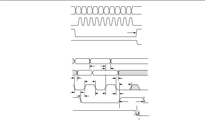
Figure 1a. Timing Diagram
SDI 1 (DATA IN) 0
SDO 1 (DATA OUT) 0
1
CLK
0
1
CS
0
VDD
VOUT
0V
Ax OR Dx |
Ax OR Dx |
|
|
|
tDS |
tDH |
|
|
|
|
|
A'x OR D'x |
A'x OR D'x |
|
|
tCH |
|
|
tPD_MAX |
|
|
tCS1 |
|
|
|
|
|
tCSH0 |
tCL |
|
tCSH1 |
|
|
||
tCSS |
|
|
|
|
|
|
tCSW |

 tS
tS 

1LSB ERROR BAND 
1LSB
Figure 1b. Detail Timing Diagram
REV. 0 |
–3– |

AD5207
ABSOLUTE MAXIMUM RATINGS1
(TA = 25°C, unless otherwise noted)
VDD to GND . . . . . . . . . . . . . . . . . . . . . . . |
. . . . . . . –0.3, +7 V |
VSS to GND . . . . . . . . . . . . . . . . . . . . . . . . |
. . . . . . . . . 0, –3 V |
VDD to VSS . . . . . . . . . . . . . . . . . . . . . . . . . |
. . . . . . . . . . . . 7 V |
VA, VB, VW to GND . . . . . . . . . . . . . . . . . . |
. . . . . . . . VSS, VDD |
IMAX2 (A, B, W) . . . . . . . . . . . . . . . . . . . . . |
. . . . . . . . ±20 mA |
Digital Inputs and Output Voltage to GND |
. . 0 V, VDD + 0.3 V |
Operating Temperature Range . . . . . . . . . |
. –40°C to +125°C |
Maximum Junction Temperature (TJ Max) |
. . . . . . . . . . 150°C |
Storage Temperature . . . . . . . . . . . . . . . . . |
. –65°C to +150°C |
Lead Temperature (Soldering, 10 sec) . . . . |
. . . . . . . . . 300°C |
Thermal Resistance3 θJA, TSSOP-14 . . . . . . |
. . . . . . . 206°C/W |
NOTES
1Stresses above those listed under Absolute Maximum Ratings may cause permanent damage to the device. This is a stress rating only; functional operation of the device at these or any other conditions above those indicated in the operational section of this specification is not implied. Exposure to absolute maximum rating conditions for extended periods may affect device reliability.
2Max current is bounded by the maximum current handling of the switches, maximum power dissipation of the package, and maximum applied voltage across any two of the A, B, and W Terminals at a given resistance. Please refer to TPC 22 for detail.
3Package Power Dissipation = (TJ Max–TA)/θJA.
PIN CONFIGURATION
VSS |
|
|
|
B1 |
1 |
|
14 |
||
B2 |
|
|
|
A1 |
2 |
|
13 |
||
A2 |
|
|
|
W1 |
3 |
AD5207 |
12 |
||
W2 |
|
|
VDD |
|
4 |
TOP VIEW |
11 |
||
DGND |
|
(Not to Scale) |
|
|
5 |
10 |
CLK |
||
|
|
|
|
|
SHDN |
6 |
|
9 |
SDO |
|
|
|
|
SDI |
CS |
7 |
|
8 |
|
|
|
|
|
|
PIN FUNCTION DESCRIPTIONS
Pin |
Mnemonic |
Description |
|
|
|
|
||||
|
|
|
|
|
||||||
1 |
VSS |
|
Negative Power Supply, specified for opera- |
|||||||
|
|
|
|
tion from 0 V to –2.7 V. |
|
|
|
|||
2 |
B2 |
|
Terminal B of RDAC#2. |
|
|
|
||||
3 |
A2 |
|
Terminal A of RDAC#2. |
|
|
|
||||
4 |
W2 |
|
Wiper, RDAC#2, addr = 12 |
|
|
|||||
5 |
DGND |
Digital Ground. |
|
|
|
|
||||
6 |
SHDN |
|
Active Low Input. Terminal A open-circuit |
|||||||
|
|
|
|
and Terminal B shorted to Wiper. Shut- |
||||||
|
|
|
|
down controls both RDACs #1 and #2. |
||||||
7 |
CS |
|
Chip Select Input, Active Low. When CS |
|||||||
|
|
|
|
returns high, data in the serial input register |
||||||
|
|
|
|
is decoded, based on the address bit, and |
||||||
|
|
|
|
loaded into the corresponding RDAC register. |
||||||
8 |
SDI |
|
Serial Data Input. MSB is loaded first. |
|
||||||
9 |
SDO |
|
Serial Data Output. Open Drain transistor |
|||||||
|
|
|
|
requires pull-up resistor. |
|
|
|
|||
10 |
CLK |
|
Serial Clock Input. Positive Edge Triggered. |
|||||||
11 |
VDD |
|
Positive Power Supply. Specified for opera- |
|||||||
|
|
|
|
tion at 2.7 V to 5.5 V. |
|
|
|
|||
12 |
W1 |
|
Wiper, RDAC #1, addr = 02. |
|
|
|||||
13 |
A1 |
|
Terminal A of RDAC #1. |
|
|
|
||||
14 |
B1 |
|
Terminal B of RDAC #1. |
|
|
|
||||
|
|
|
|
|
|
|
||||
|
|
|
Table I. Serial-Data Word Format |
|
|
|||||
|
|
|
|
|
|
|
|
|
|
|
ADDR |
|
|
|
|
DATA |
|
|
|
|
|
B9 |
B8 |
|
B7 |
B6 |
B5 |
B4 |
B3 |
B2 |
B1 |
B0 |
|
|
|
|
|
|
|
|
|
|
|
A1 |
A0 |
|
D7 |
D6 |
D5 |
D4 |
D3 |
D2 |
D1 |
D0 |
|
|
|
MSB |
|
|
|
|
|
|
LSB |
29 |
28 |
|
27 |
|
|
|
|
|
|
20 |
NOTES
ADDR(RDAC1) = 00; ADDR(RDAC2 = 01).
Data loads B9 first into SDI pin.
ORDERING GUIDE
|
|
Temperature |
Package |
Package |
Qty Per |
Branding |
Model |
k |
Range |
Description |
Option |
Container |
Information* |
|
|
|
|
|
|
|
AD5207BRU10-REEL7 |
10 |
–40°C to +125°C |
TSSOP-14 |
RU-14 |
1,000 |
B10 |
AD5207BRU50-REEL7 |
50 |
–40°C to +125°C |
TSSOP-14 |
RU-14 |
1,000 |
B50 |
AD5207BRU100-REEL7 |
100 |
–40°C to +125°C |
TSSOP-14 |
RU-14 |
1,000 |
B100 |
|
|
|
|
|
|
|
*Three lines of information appear on the device. Line 1 lists the part number; Line 2 includes branding information and the ADI logo, and Line 3 contains the date code YYWW.
CAUTION
ESD (electrostatic discharge) sensitive device. Electrostatic charges as high as 4000 V readily accumulate on the human body and test equipment and can discharge without detection. Although the AD5207 features proprietary ESD protection circuitry, permanent damage may occur on devices subjected to high-energy electrostatic discharges. Therefore, proper ESD precautions are recommended to avoid performance degradation or loss of functionality.
WARNING!
ESD SENSITIVE DEVICE
–4– |
REV. 0 |

Typical Performance Characteristics–AD5207
|
0.20 |
|
|
|
|
|
|
|
|
|
|
|
|
|
|
|
VDD = 5.5V,V SS = 0V |
||
|
0.15 |
|
|
|
|
|
|
|
|
|
0.10 |
|
|
|
|
|
|
|
|
– LSB |
0.05 |
|
|
|
|
|
|
|
|
0.00 |
|
|
|
|
|
|
|
|
|
RDNL |
|
|
|
|
|
|
|
|
|
0.05 |
|
|
|
|
|
|
|
|
|
|
|
|
|
|
|
|
|
|
|
|
0.10 |
|
|
|
|
|
|
|
|
|
0.15 |
|
|
|
|
|
|
|
|
|
0.20 |
32 |
64 |
96 |
128 |
160 |
192 |
224 |
256 |
|
0 |
||||||||
CODE – Decimal
TPC 1. 10 kΩ RDNL vs. Code
|
0.20 |
|
|
|
|
|
|
|
|
|
|
|
|
|
|
|
VDD = 5.5V,V SS = 0V |
||
|
0.15 |
|
|
|
|
|
|
|
|
|
0.10 |
|
|
|
|
|
|
|
|
– LSB |
0.05 |
|
|
|
|
|
|
|
|
0.00 |
|
|
|
|
|
|
|
|
|
RINL |
|
|
|
|
|
|
|
|
|
–0.05 |
|
|
|
|
|
|
|
|
|
|
|
|
|
|
|
|
|
|
|
|
–0.10 |
|
|
|
|
|
|
|
|
|
–0.15 |
|
|
|
|
|
|
|
|
|
–0.20 |
|
|
|
|
|
|
|
|
|
0 |
32 |
64 |
96 |
128 |
160 |
192 |
224 |
256 |
CODE – Decimal
TPC 2. 10 kΩ RINL vs. Code
0.3 |
|
|
|
|
|
|
|
|
|
|
|
|
|
|
VDD = 5.5V,V SS = 0V |
|
|
0.2 |
|
|
|
|
|
|
|
|
0.1 |
|
|
|
|
|
|
|
|
–LSB |
|
|
|
|
|
|
|
|
0.0 |
|
|
|
|
|
|
|
|
DNL |
|
|
|
|
|
|
|
|
–0.1 |
|
|
|
|
|
|
|
|
–0.2 |
|
|
|
|
|
|
|
|
–0.3 |
|
|
|
|
|
|
|
|
0 |
32 |
64 |
96 |
128 |
160 |
192 |
224 |
256 |
CODE – Decimal
TPC 3. 10 kΩ DNL vs. Code
|
0.4 |
|
|
|
|
|
|
|
|
|
0.3 |
|
|
|
|
|
VDD = 5.5V,V SS = 0V |
|
|
|
|
|
|
|
|
|
|
|
|
|
0.2 |
|
|
|
|
|
|
|
|
– LSB |
0.1 |
|
|
|
|
|
|
|
|
0.0 |
|
|
|
|
|
|
|
|
|
INL |
–0.1 |
|
|
|
|
|
|
|
|
|
|
|
|
|
|
|
|
|
|
|
–0.2 |
|
|
|
|
|
|
|
|
|
–0.3 |
|
|
|
|
|
|
|
|
|
–0.4 |
|
|
|
|
|
|
|
|
|
0 |
32 |
64 |
96 |
128 |
160 |
192 |
224 |
256 |
CODE – Decimal
TPC 4. 10 kΩ INL vs. Code
1.0 |
|
|
|
|
|
|
|
|
IDD @ VDD/VSS = 5V/0V |
|
|
0.1 |
|
|
|
|
|
– mA |
|
IDD @ VDD/VSS = 2.5V |
|
|
|
SS |
|
|
|
||
/I |
|
|
|
|
|
DD |
|
|
|
|
|
I |
|
|
|
|
|
0.01 |
|
|
|
|
|
|
ISS @ VDD/VSS = 2.5V |
IDD @ V DD/VSS = 3V/0V |
|
||
|
|
|
|
||
0.001 |
|
|
|
|
|
0.0 |
1.0 |
2.0 |
3.0 |
4.0 |
5.0 |
|
|
VIH – V |
|
|
|
TPC 5. Supply Current vs. Logic Input Voltage
|
20 |
|
|
|
|
|
|
|
|
|
|
|
|
|
|
|
|
|
|
|
18 |
|
|
|
|
|
|
|
|
|
|
|
|
|
VIL = VSS |
|
|
|
|
|
|
|
|
|
|
|
|
|
|
|
|
|
|
VIH = VDD |
|
|
|
||
|
|
|
|
|
|
|
|
|
|
|
|
|
|
|
|
|
|||
– A |
16 |
|
|
|
|
|
|
|
|
|
|
|
|
|
|
|
|
|
|
|
|
|
|
|
|
|
|
|
|
|
|
|
|
|
|
|
|
||
14 |
|
|
|
|
|
|
|
|
|
|
|
|
|
|
|
|
|
|
|
|
|
|
|
|
|
|
VDD |
= 5.5V |
|
|
|
|
|
|
|
||||
|
|
|
|
|
|
|
|
|
|
|
|
|
|
|
|||||
CURRENT |
12 |
|
|
|
|
|
|
|
|
|
|
|
|
|
|
|
|
|
|
|
|
|
|
|
|
|
|
|
|
|
|
|
|
|
|
|
|
||
|
|
|
|
|
|
|
|
|
|
|
|
|
|
|
|
|
|
|
|
SUPPLY |
10 |
|
|
|
|
|
|
|
|
|
|
|
|
|
|
|
|
|
|
|
|
|
|
|
|
|
|
|
|
|
|
|
|
|
|
|
|
||
8 |
|
|
|
|
|
|
|
|
|
|
|
|
|
|
|
|
|
|
|
|
|
|
|
|
|
|
|
|
|
|
|
|
|
|
|
|
|
|
|
|
6 |
|
|
|
|
|
|
|
VDD = 2.7V |
|
|
|
|
|
|
|
|
||
DD |
|
|
|
|
|
|
|
|
|
|
|
|
|
|
|
|
|
|
|
I |
4 |
|
|
|
|
|
|
|
|
|
|
|
|
|
|
|
|
|
|
|
|
|
|
|
|
|
|
|
|
|
|
|
|
|
|
|
|
|
|
|
|
|
|
|
|
|
|
|
|
|
|
|
|
|
|
|
|
|
|
|
2 |
|
|
|
|
|
|
|
|
|
|
|
|
|
|
|
|
|
|
|
|
|
|
|
|
|
|
|
|
|
|
|
|
|
|
|
|
|
|
|
0 |
|
|
|
|
|
|
|
|
|
|
|
|
|
|
|
|
|
|
|
|
|
|
|
|
|
|
|
|
|
|
|
|
|
|
|
|
|
|
|
–40 |
–20 |
0 |
20 |
40 |
|
60 |
80 |
100 |
||||||||||
TEMPERATURE – C
TPC 6. Supply Current vs. Temperature
REV. 0 |
–5– |
Loading...