


 Loading...
8-Channel DAC with PLL and Single-Ended Outputs, 192 kHz, 24 Bits
FEATURES
PLL generated or direct master clock Low EMI design
108 dB DAC dynamic range and SNR −94 dB THD + N
Single 3.3 V supply Tolerance for 5 V logic inputs
Supports 24 bits and 8 kHz to 192 kHz sample rates Single-ended DAC output
Log volume control with autoramp function SPI® controllable for flexibility Software-controllable clickless mute Software power-down
Right-justified, left-justified, I2S, and TDM modes Master and slave modes up to 16-channel in/out 48-lead LQFP
Qualified for automotive applications
APPLICATIONS
Automotive audio systems
Home theater systems
Set-top boxes
Digital audio effects processors
AD1934
GENERAL DESCRIPTION
The AD1934 is a high performance, single chip that provides eight digital-to-analog converters (DACs) with single-ended output using the Analog Devices, Inc., patented multibit sigmadelta (Σ-Δ) architecture. An SPI port is included, allowing a microcontroller to adjust volume and many other parameters. The AD1934 operates from 3.3 V digital and analog supplies. The AD1934 is available in a 48-lead (single-ended output) LQFP. Other members of this family include a differential DAC output version.
The AD1934 is designed for low EMI. This consideration is apparent in both the system and circuit design architectures. By using the on-board PLL to derive the master clock from the LR clock or from an external crystal, the AD1934 eliminates the need for a separate high frequency master clock and can also be used with a suppressed bit clock. The DACs are designed using
the latest Analog Devices continuous time architectures to further minimize EMI. By using 3.3 V supplies, power consumption is minimized, further reducing emissions.
FUNCTIONAL BLOCK DIAGRAM
|
AD1934 |
|
|
|
DAC |
|
|
|
|
|
|
DAC |
|
|
|
|
|
DIGITAL |
DAC |
|
|
|
|
|
DAC |
ANALOG |
|
|
|
|
|
FILTER |
||
|
|
|
|
AND |
DAC |
AUDIO |
|
|
CLOCKS |
|
VOLUME |
OUTPUTS |
|
|
|
|
CONTROL |
DAC |
|
|
DIGITAL AUDIO |
SERIAL |
|
TIMING MANAGEMENT |
|
|
|
DATA |
|
AND CONTROL |
|
|
|
|
INPUT/OUTPUT |
SDATAIN |
|
DAC |
|
||
PORT |
(CLOCK AND PLL) |
|
|
|||
|
|
|
|
|
DAC |
|
|
PRECISION |
|
CONTROL PORT |
6.144MHz |
|
|
|
VOLTAGE |
|
|
|
|
|
|
|
SPI |
|
|
|
|
|
REFERENCE |
|
|
|
|
|
|
|
|
|
|
|
|
|
|
|
CONTROL DATA |
|
|
06106-001 |
|
|
|
INPUT/OUTPUT |
|
|
Figure 1.
Rev. C
Information furnished by Analog Devices is believed to be accurate and reliable. However, no responsibilityisassumedbyAnalogDevicesforitsuse,norforanyinfringementsofpatentsorother rightsofthirdpartiesthatmayresultfromitsuse.Specificationssubjecttochangewithoutnotice.No license is granted by implication or otherwise under any patent or patent rights of Analog Devices. Trademarksandregisteredtrademarksarethepropertyoftheirrespectiveowners.
One Technology Way, P.O. Box 9106, Norwood, MA 02062-9106, U.S.A. Tel: 781.329.4700 www.analog.com Fax: 781.461.3113 ©2007–2011 Analog Devices, Inc. All rights reserved.

AD1934
TABLE OF CONTENTS |
|
Features .............................................................................................. |
1 |
Applications....................................................................................... |
1 |
General Description ......................................................................... |
1 |
Functional Block Diagram .............................................................. |
1 |
Revision History ............................................................................... |
2 |
Specifications..................................................................................... |
3 |
Test Conditions............................................................................. |
3 |
Analog Performance Specifications ........................................... |
3 |
Crystal Oscillator Specifications................................................. |
4 |
Digital Input/Output Specifications........................................... |
4 |
Power Supply Specifications........................................................ |
5 |
Digital Filters................................................................................. |
6 |
Timing Specifications .................................................................. |
6 |
Absolute Maximum Ratings............................................................ |
8 |
Thermal Resistance ...................................................................... |
8 |
ESD Caution.................................................................................. |
8 |
Pin Configuration and Function Descriptions............................. |
9 |
Typical Performance Characteristics ........................................... |
11 |
Theory of Operation ...................................................................... |
12 |
REVISION HISTORY |
|
7/11—Rev. B to Rev. C |
|
Deleted References to I2C ............................................. |
Throughout |
Changes to Figure 2 and Table 10, DSDATAx/AUXDATA1 Pin |
|
Descriptions ...................................................................................... |
9 |
1/11—Rev. A to Rev. B |
|
Added Automotive Information.................................. |
Throughout |
Change to Table 2, Introductory Text ............................................ |
4 |
Change to Table 4, Introductory Text ............................................ |
4 |
Change to Table 7, Introductory Text ............................................ |
6 |
Digital-to-Analog Converters (DACs) .................................... |
12 |
Clock Signals............................................................................... |
12 |
Reset and Power-Down ............................................................. |
12 |
Serial Control Port ..................................................................... |
13 |
Power Supply and Voltage Reference....................................... |
14 |
Serial Data Ports—Data Format............................................... |
14 |
Time-Division Multiplexed (TDM) Modes............................ |
14 |
Daisy-Chain Mode ..................................................................... |
16 |
Control Registers ............................................................................ |
20 |
Definitions................................................................................... |
20 |
PLL and Clock Control Registers............................................. |
20 |
DAC Control Registers .............................................................. |
21 |
Auxiliary TDM Port Control Registers ................................... |
23 |
Additional Modes....................................................................... |
23 |
Application Circuits ....................................................................... |
25 |
Outline Dimensions ....................................................................... |
26 |
Ordering Guide .......................................................................... |
26 |
Automotive Products................................................................. |
26 |
Changes to Ordering Guide .......................................................... |
26 |
9/09—Rev. 0 to Rev. A |
|
Change to Title................................................................................... |
1 |
Change to Table 11 ......................................................................... |
13 |
Change to Power Supply and Voltage Reference Section.......... |
14 |
Updated Outline Dimensions....................................................... |
26 |
Changes to Ordering Guide .......................................................... |
26 |
8/07—Revision 0: Initial Version |
|
Rev. C | Page 2 of 28

AD1934
SPECIFICATIONS
TEST CONDITIONS
Performance of all channels is identical, exclusive of the interchannel gain mismatch and interchannel phase deviation specifications.
Supply Voltages (AVDD, DVDD) |
3.3 V |
Temperature Range1 |
As specified in Table 1 and Table 2 |
Master Clock |
12.288 MHz (48 kHz fS, 256 × fS mode) |
Input Sample Rate |
48 kHz |
Measurement Bandwidth |
20 Hz to 20 kHz |
Word Width |
24 bits |
Load Capacitance (Digital Output) |
20 pF |
Load Current (Digital Output) |
±1 mA or 1.5 kΩ to ½ DVDD supply |
Input Voltage HI |
2.0 V |
Input Voltage LO |
0.8 V |
1 Functionally guaranteed at −40°C to +125°C case temperature.
ANALOG PERFORMANCE SPECIFICATIONS
Specifications guaranteed at 25°C (ambient).
Table 1.
Parameter |
Test Conditions/Comments |
Min |
Typ |
Max |
Unit |
|
|
|
|
|
|
DIGITAL-TO-ANALOG CONVERTERS |
|
|
|
|
|
Dynamic Range |
20 Hz to 20 kHz, −60 dB input |
|
|
|
|
No Filter (RMS) |
|
98 |
104 |
|
dB |
With A-Weighted Filter (RMS) |
|
100 |
106 |
|
dB |
With A-Weighted Filter (Average) |
|
|
108 |
|
dB |
Total Harmonic Distortion + Noise |
0 dBFS |
|
|
|
|
Single-Ended Version |
Two channels running |
|
−92 |
|
dB |
|
Eight channels running |
|
−86 |
−75 |
dB |
Full-Scale Output Voltage |
|
|
0.88 (2.48) |
|
V rms (V p-p) |
Gain Error |
|
−10 |
|
+10 |
% |
Interchannel Gain Mismatch |
|
−0.2 |
|
+0.2 |
dB |
Offset Error |
|
−16 |
−4 |
+16 |
mV |
Gain Drift |
|
−30 |
|
+30 |
ppm/°C |
Interchannel Isolation |
|
|
100 |
|
dB |
Interchannel Phase Deviation |
|
|
0 |
|
Degrees |
Volume Control Step |
|
|
0.375 |
|
dB |
Volume Control Range |
|
|
95 |
|
dB |
De-emphasis Gain Error |
|
|
|
±0.6 |
dB |
Output Resistance at Each Pin |
|
|
100 |
|
Ω |
REFERENCE |
|
|
|
|
|
Internal Reference Voltage |
FILTR pin |
|
1.50 |
|
V |
External Reference Voltage |
FILTR pin |
1.32 |
1.50 |
1.68 |
V |
Common-Mode Reference Output |
CM pin |
|
1.50 |
|
V |
|
|
|
|
|
|
Rev. C | Page 3 of 28

AD1934
Specifications measured at 125°C (case).
Table 2.
Parameter |
Test Conditions/Comments |
Min |
Typ |
Max |
Unit |
DIGITAL-TO-ANALOG CONVERTERS |
|
|
|
|
|
Dynamic Range |
20 Hz to 20 kHz, −60 dB input |
|
|
|
|
No Filter (RMS) |
|
98 |
104 |
|
dB |
With A-Weighted Filter (RMS) |
|
100 |
106 |
|
dB |
With A-Weighted Filter (Average) |
|
|
108 |
|
dB |
Total Harmonic Distortion + Noise |
0 dBFS |
|
|
|
|
Single-Ended Version |
Two channels running |
|
−92 |
|
dB |
|
Eight channels running |
|
−86 |
−70 |
dB |
Full-Scale Output Voltage |
|
|
0.8775 (2.482) |
|
V rms (V p-p) |
Gain Error |
|
−10 |
|
+10 |
% |
Interchannel Gain Mismatch |
|
−0.2 |
|
+0.2 |
dB |
Offset Error |
|
−16 |
−4 |
+16 |
mV |
Gain Drift |
|
−30 |
|
+30 |
ppm/°C |
REFERENCE |
|
|
|
|
|
Internal Reference Voltage |
FILTR pin |
|
1.50 |
|
V |
External Reference Voltage |
FILTR pin |
1.32 |
1.50 |
1.68 |
V |
Common-Mode Reference Output |
CM pin |
|
1.50 |
|
V |
|
|
|
|
|
|
CRYSTAL OSCILLATOR SPECIFICATIONS
Table 3.
Parameter |
Min |
Typ |
Max |
Unit |
|
|
|
|
|
Transconductance |
|
3.5 |
|
mmhos |
DIGITAL INPUT/OUTPUT SPECIFICATIONS
−40°C < TC < 125°C, DVDD = 3.3 V ± 10%.
Table 4.
Parameter |
Test Conditions/Comments |
Min |
Typ |
Max |
Unit |
|
|
|
|
|
|
Input Voltage HI (VIH) |
|
2.0 |
|
|
V |
Input Voltage HI (VIH) |
MCLKI pin |
2.2 |
|
|
V |
Input Voltage LO (VIL) |
|
|
|
0.8 |
V |
Input Leakage |
IIH @ VIH = 2.4 V |
|
|
10 |
μA |
|
IIL @ VIL = 0.8 V |
|
|
10 |
μA |
High Level Output Voltage (VOH) |
IOH = 1 mA |
DVDD − 0.60 |
|
|
V |
Low Level Output Voltage (VOL) |
IOL = 1 mA |
|
|
0.4 |
V |
Input Capacitance |
|
|
|
5 |
pF |
Rev. C | Page 4 of 28

|
|
|
|
|
|
AD1934 |
|
|
|
|
|
|
|
|
|
POWER SUPPLY SPECIFICATIONS |
|
|
|
|
|
|
|
Table 5. |
|
|
|
|
|
|
|
Parameter |
|
Test Conditions/Comments |
Min |
Typ |
Max |
|
Unit |
|
|
|
|
|
|
|
|
SUPPLIES |
|
|
|
|
|
|
|
Voltage |
|
|
|
|
|
|
|
|
|
DVDD |
3.0 |
3.3 |
3.6 |
|
V |
|
|
AVDD |
3.0 |
3.3 |
3.6 |
|
V |
Digital Current |
|
MCLK = 256 fS |
|
|
|
|
|
Normal Operation |
|
fS = 48 kHz |
|
56 |
|
|
mA |
|
|
fS = 96 kHz |
|
65 |
|
|
mA |
|
|
fS = 192 kHz |
|
95 |
|
|
mA |
Power-Down |
|
fS = 48 kHz to 192 kHz |
|
2.0 |
|
|
mA |
Analog Current |
|
|
|
|
|
|
|
Normal Operation |
|
|
|
74 |
|
|
mA |
Power-Down |
|
|
|
23 |
|
|
mA |
|
|
|
|
|
|
|
|
DISSIPATION |
|
|
|
|
|
|
|
Operation |
|
MCLK = 256 fS, 48 kHz |
|
|
|
|
|
All Supplies |
|
|
|
429 |
|
|
mW |
Digital Supply |
|
|
|
185 |
|
|
mW |
Analog Supply |
|
|
|
244 |
|
|
mW |
Power-Down, All Supplies |
|
|
|
83 |
|
|
mW |
POWER SUPPLY REJECTION RATIO |
|
|
|
|
|
|
|
Signal at Analog Supply Pins |
|
1 kHz, 200 mV p-p |
|
50 |
|
|
dB |
|
|
20 kHz, 200 mV p-p |
|
50 |
|
|
dB |
|
|
|
|
|
|
|
|
Rev. C | Page 5 of 28

AD1934
DIGITAL FILTERS
Table 6.
Parameter |
Mode |
Factor |
Min |
Typ |
Max |
Unit |
DAC INTERPOLATION FILTER |
|
|
|
|
|
|
Pass Band |
48 kHz mode, typ @ 48 kHz |
0.4535 fS |
|
22 |
|
kHz |
|
96 kHz mode, typ @ 96 kHz |
0.3646 fS |
35 |
|
|
kHz |
|
192 kHz mode, typ @ 192 kHz |
0.3646 fS |
|
70 |
|
kHz |
Pass-Band Ripple |
48 kHz mode, typ @ 48 kHz |
|
|
|
±0.01 |
dB |
|
96 kHz mode, typ @ 96 kHz |
|
|
|
±0.05 |
dB |
|
192 kHz mode, typ @ 192 kHz |
|
|
|
±0.1 |
dB |
Transition Band |
48 kHz mode, typ @ 48 kHz |
0.5 fS |
|
24 |
|
kHz |
|
96 kHz mode, typ @ 96 kHz |
0.5 fS |
|
48 |
|
kHz |
|
192 kHz mode, typ @ 192 kHz |
0.5 fS |
|
96 |
|
kHz |
Stop Band |
48 kHz mode, typ @ 48 kHz |
0.5465 fS |
|
26 |
|
kHz |
|
96 kHz mode, typ @ 96 kHz |
0.6354 fS |
|
61 |
|
kHz |
|
192 kHz mode, typ @ 192 kHz |
0.6354 fS |
|
122 |
|
kHz |
Stop-Band Attenuation |
48 kHz mode, typ @ 48 kHz |
|
70 |
|
|
dB |
|
96 kHz mode, typ @ 96 kHz |
|
70 |
|
|
dB |
|
192 kHz mode, typ @ 192 kHz |
|
70 |
|
|
dB |
Group Delay |
48 kHz mode, typ @ 48 kHz |
25/fS |
|
521 |
|
μs |
|
96 kHz mode, typ @ 96 kHz |
11/fS |
|
115 |
|
μs |
|
192 kHz mode, typ @ 192 kHz |
8/fS |
|
42 |
|
μs |
TIMING SPECIFICATIONS
−40°C < TC < 125°C, DVDD = 3.3 V ± 10%.
Table 7.
Parameter |
Condition |
Comments |
Min |
Max |
Unit |
||||
|
|
|
|
|
|
|
|
|
|
INPUT MASTER CLOCK (MCLK) AND RESET |
|
|
|
|
|
|
|
|
|
tMH |
|
MCLK duty cycle |
DAC clock source = PLL clock @ 256 fS, |
40 |
60 |
% |
|||
|
|
|
|
|
|
384 fS, 512 fS, 768 fS |
|
|
|
tMH |
|
|
|
|
|
DAC clock source = direct MCLK @ 512 fS |
40 |
60 |
% |
|
|
|
|
|
|
(bypass on-chip PLL) |
|
|
|
fMCLK |
|
MCLK frequency |
PLL mode, 256 fS reference |
6.9 |
13.8 |
MHz |
|||
fMCLK |
|
|
|
|
|
Direct 512 fS mode |
|
27.6 |
MHz |
tPDR |
|
|
low |
|
15 |
|
ns |
||
|
RST |
|
|
|
|||||
tPDRR |
|
|
|
Reset to active output |
4096 |
|
tMCLK |
||
|
RST |
recovery |
|
||||||
|
|
|
|
|
|
|
|
|
|
PLL |
|
|
|
|
|
|
|
|
|
Lock Time |
|
MCLK and LRCLK input |
|
|
10 |
ms |
|||
256 fS VCO Clock, Output Duty Cycle |
|
|
|
|
|
|
40 |
60 |
% |
MCLKO Pin |
|
|
|
|
|
|
|
|
|
SPI PORT |
|
|
|
|
|
See Figure 9 |
|
|
|
tCCH |
|
CCLK high |
|
35 |
|
ns |
|||
tCCL |
|
CCLK low |
|
35 |
|
ns |
|||
fCCLK |
|
CCLK frequency |
fCCLK = 1/tCCP, only tCCP shown in Figure 9 |
|
10 |
MHz |
|||
tCDS |
|
CDATA setup |
To CCLK rising |
10 |
|
ns |
|||
tCDH |
|
CDATA hold |
From CCLK rising |
10 |
|
ns |
|||
tCLS |
|
|
To CCLK rising |
10 |
|
ns |
|||
|
CLATCH |
setup |
|
||||||
tCLH |
|
|
From CCLK falling |
10 |
|
ns |
|||
|
CLATCH |
hold |
|
||||||
tCLHIGH |
|
|
Not shown in Figure 9 |
10 |
|
ns |
|||
|
CLATCH |
high |
|
||||||
tCOE |
|
COUT enable |
From CCLK falling |
|
30 |
ns |
|||
tCOD |
|
COUT delay |
From CCLK falling |
|
30 |
ns |
|||
tCOH |
|
COUT hold |
From CCLK falling, not shown in Figure 9 |
30 |
|
ns |
|||
tCOTS |
|
COUT tri-state |
From CCLK falling |
|
30 |
ns |
|||
|
|
|
|
|
|
|
|
|
|
Rev. C | Page 6 of 28

AD1934
Parameter |
Condition |
Comments |
Min |
Max |
Unit |
DAC SERIAL PORT |
|
See Figure 16 |
|
|
|
tDBH |
DBCLK high |
Slave mode |
10 |
|
ns |
tDBL |
DBCLK low |
Slave mode |
10 |
|
ns |
tDLS |
DLRCLK setup |
To DBCLK rising, slave mode |
10 |
|
ns |
tDLH |
DLRCLK hold |
From DBCLK rising, slave mode |
5 |
|
ns |
tDLS |
DLRCLK skew |
From DBCLK falling, master mode |
−8 |
+8 |
ns |
tDDS |
DSDATA setup |
To DBCLK rising |
10 |
|
ns |
tDDH |
DSDATA hold |
From DBCLK rising |
5 |
|
ns |
|
|
|
|
|
|
AUXTDM SERIAL PORT |
|
See Figure 17 |
|
|
|
tABH |
AUXTDMBCLK high |
Slave mode |
10 |
|
ns |
tABL |
AUXTDMBCLK low |
Slave mode |
10 |
|
ns |
tALS |
AUXTDMLRCLK setup |
To AUXTDMBCLK rising, slave mode |
10 |
|
ns |
tALH |
AUXTDMLRCLK hold |
From AUXTDMBCLK rising, slave mode |
5 |
|
ns |
tALS |
AUXTDMLRCLK skew |
From AUXTDMBCLK falling, master mode |
−8 |
+8 |
ns |
tDDS |
DSDATA setup |
To AUXTDMBCLK, not shown in Figure 17 |
10 |
|
ns |
tDDH |
DSDATA hold |
From AUXTDMBCLK rising, not shown in |
5 |
|
ns |
|
|
Figure 17 |
|
|
|
AUXILIARY INTERFACE |
|
|
|
|
|
tDXDD |
AUXDATA delay |
From AUXBCLK falling |
|
18 |
ns |
tXBH |
AUXBCLK high |
|
10 |
|
ns |
tXBL |
AUXBCLK low |
|
10 |
|
ns |
tDLS |
AUXLRCLK setup |
To AUXBCLK rising |
10 |
|
ns |
tDLH |
AUXLRCLK hold |
From AUXBCLK rising |
5 |
|
ns |
Rev. C | Page 7 of 28

AD1934
ABSOLUTE MAXIMUM RATINGS
Table 8.
Parameter |
Rating |
|
|
Analog (AVDD) |
−0.3 V to +3.6 V |
Digital (DVDD) |
−0.3 V to +3.6 V |
Input Current (Except Supply Pins) |
±20 mA |
Analog Input Voltage (Signal Pins) |
−0.3 V to AVDD + 0.3 V |
Digital Input Voltage (Signal Pins) |
−0.3 V to DVDD + 0.3 V |
Operating Temperature Range (Case) |
−40°C to +125°C |
Storage Temperature Range |
−65°C to +150°C |
Stresses above those listed under Absolute Maximum Ratings may cause permanent damage to the device. This is a stress rating only; functional operation of the device at these or any other conditions above those indicated in the operational section of this specification is not implied. Exposure to absolute maximum rating conditions for extended periods may affect device reliability.
THERMAL RESISTANCE
θJA represents thermal resistance, junction-to-ambient; θJC represents the thermal resistance, junction-to-case. All characteristics are for a 4-layer board.
Table 9. Thermal Resistance
Package Type |
θJA |
θJC |
Unit |
|
|
|
|
48-Lead LQFP |
50.1 |
17 |
°C/W |
|
|
|
|
ESD CAUTION
Rev. C | Page 8 of 28
AD1934
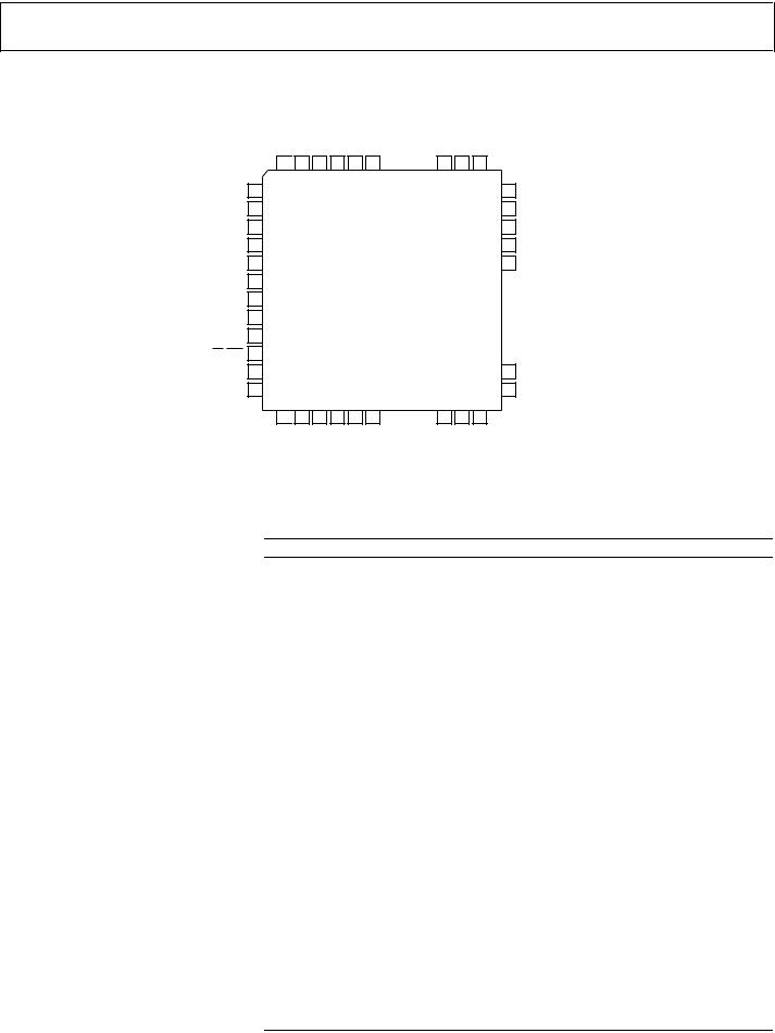
PIN CONFIGURATION AND FUNCTION DESCRIPTIONS
AGND 1 

MCLKI/XI 2
MCLKO/XO 3
AGND 4
AVDD 5
OL3 6
OR3 7
OL4 8
OR4 9
PD/RST 10
DSDATA4 11
DGND 12
NC = NO CONNECT
AVDD |
LF |
NC |
NC |
NC |
NC |
NC |
NC |
|
NC |
NC |
CM |
AVDD |
|
|
|
|||
|
|
|
|
|
|
|
|
|
|
|
|
|
|
|
|
|
|
|
48 |
47 |
46 |
45 |
44 |
43 |
42 |
|
|
41 |
|
40 |
39 |
38 |
37 |
|
|
|
|
|
|
|
|
|
|
|
|
|
|
|
|
|
|
36 |
AGND |
|||
|
|
|
|
|
|
|
|
|
|
|
|
|
|
35 |
FILTR |
|||
|
|
|
|
|
|
|
|
|
|
|
|
|
|
34 |
AGND |
|||
|
|
|
|
|
|
|
|
|
|
|
|
|
|
33 |
AVDD |
|||
|
|
|
|
|
AD1934 |
|
|
|
|
|
32 |
AGND |
||||||
|
|
|
|
|
TOP VIEW |
|
|
|
|
|
|
31 |
OR2 |
|||||
|
|
|
|
(Not to Scale) |
|
|
|
|
|
|
OL2 |
|||||||
|
|
|
|
|
|
|
|
|
30 |
|||||||||
|
|
|
|
SINGLE-ENDED |
|
|
|
|
|
|||||||||
|
|
|
|
|
|
|
|
|
|
|
|
|
||||||
|
|
|
|
|
OUTPUT |
|
|
|
|
|
|
29 |
OR1 |
|||||
|
|
|
|
|
|
|
|
|
|
|
|
|
|
|
OL1 |
|||
|
|
|
|
|
|
|
|
|
|
|
|
|
|
|
28 |
|||
|
|
|
|
|
|
|
|
|
|
|
|
|
|
|
|
|
|
|
|
|
|
|
|
|
|
|
|
|
|
|
|
|
|
27 |
|
CLATCH |
|
|
|
|
|
|
|
|
|
|
|
|
|
|
|
26 |
CCLK |
|||
|
|
|
|
|
|
|
|
|
|
|
|
|
|
25 |
DGND |
|||
|
|
|
|
|
|
|
|
|
|
|
|
|
|
|
|
|
|
|
13 |
14 |
15 |
16 |
17 |
18 |
19 |
|
|
20 |
|
21 |
22 |
23 |
24 |
|
|
|
|
DVDD |
DSDATA3 |
DSDATA2 |
DSDATA1 |
DBCLK |
DLRCLK |
AUXDATA1 |
NC |
|
AUXTDMBCLK |
AUXTDMLRCLK |
CIN |
COUT |
06106-020 |
|||||
|
|
|
|
|
|
|
Figure 2. Pin Configuration |
Table 10. Pin Function Description |
|
||||||
Pin No. |
Input/Output |
|
Mnemonic |
Description |
|||
|
|
|
|
|
|
|
|
1 |
I |
AGND |
Analog Ground. |
||||
2 |
I |
MCLKI/XI |
Master Clock Input/Crystal Oscillator Input. |
||||
3 |
O |
|
MCLKO/XO |
Master Clock Output/Crystal Oscillator Output. |
|||
4 |
I |
AGND |
Analog Ground. |
||||
5 |
I |
AVDD |
Analog Power Supply. Connect to analog 3.3 V supply. |
||||
6 |
O |
|
OL3 |
DAC 3 Left Output. |
|||
7 |
O |
|
OR3 |
DAC 3 Right Output. |
|||
8 |
O |
|
OL4 |
DAC 4 Left Output. |
|||
9 |
O |
|
OR4 |
DAC 4 Right Output. |
|||
10 |
I |
|
|
|
|
|
Power-Down Reset (Active Low). |
|
PD/RST |
||||||
11 |
I/O |
|
DSDATA4 |
DAC Serial Data Input 4. Data input to DAC4 data in/TDM DAC2 data out (dual-line |
|||
|
|
|
|
|
|
|
mode)/AUX DAC2 data out (to external DAC2). |
12 |
I |
DGND |
Digital Ground. |
||||
13 |
I |
DVDD |
Digital Power Supply. Connect to digital 3.3 V supply. |
||||
14 |
I/O |
|
DSDATA3 |
DAC Serial Data Input 3. Data input to DAC3 data in/TDM DAC2 data in (dual-line |
|||
|
|
|
|
|
|
|
mode)/AUX not used. |
15 |
I/O |
|
DSDATA2 |
DAC Serial Data Input 2. Data input to DAC2 data in/TDM DAC2 data out/AUX not used. |
|||
16 |
I |
|
DSDATA1 |
DAC Serial Data Input 1. Data input to DAC1 data in/TDM DAC data in/AUX TDM data in. |
|||
17 |
I/O |
|
DBCLK |
Bit Clock for DACs (Regular Stereo, TDM, or Daisy-Chain TDM Mode). |
|||
18 |
I/O |
|
DLRCLK |
LR Clock for DACs (Regular Stereo, TDM, or Daisy-Chain TDM Mode). |
|||
19 |
O |
|
AUXDATA1 |
AUX DAC1 data out (to external DAC1). |
|||
20 |
|
NC |
No Connect. |
||||
21 |
I/O |
|
AUXTDMBCLK |
Auxiliary Mode Only DAC TDM Bit Clock. |
|||
22 |
I/O |
|
AUXTDMLRCLK |
Auxiliary Mode Only DAC LR TDM Clock. |
|||
23 |
I |
|
CIN/ADR0 |
Control Data Input (SPI). |
|||
24 |
I/O |
|
COUT/SDA |
Control Data Output (SPI). |
|||
25 |
I |
DGND |
Digital Ground. |
||||
|
|
|
|
|
|
|
|
Rev. C | Page 9 of 28
Loading...