


AD420AR-32
Table of contents
 Loading...
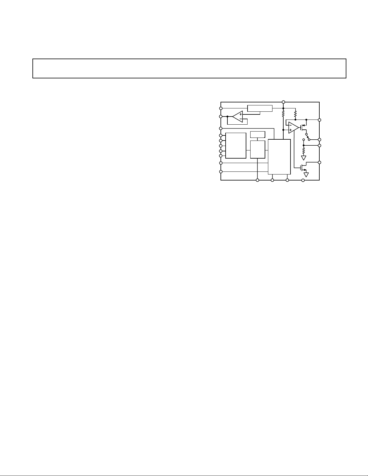
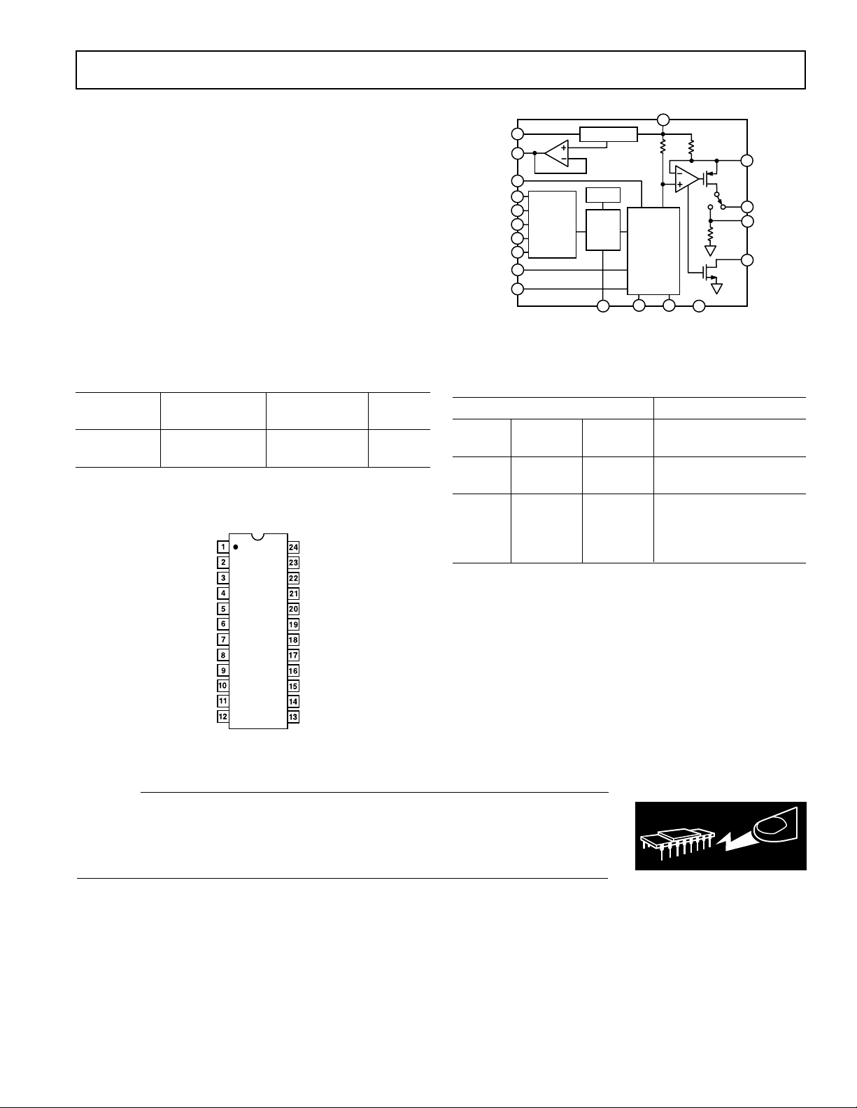
FUNCTIONAL BLOCK DIAGRAM
AD420
V
CC
4kV
40V
BOOST
I
OUT
V
OUT
FAULT
DETECT
GNDCAP 1
OFFSET
TRIM
V
LL
REF OUT
REF IN
DATA OUT
CLEAR
LATCH
CLOCK
DATA IN
RANGE
SELECT 1
RANGE
SELECT 2
1.25kV
REFERENCE
CLOCK
16-BIT
DAC
DATA I/P
REGISTER
SWITCHED
CURRENT
SOURCES
AND
FILTERING
CAP 2
REV. F
Information furnished by Analog Devices is believed to be accurate and
reliable. However, no responsibility is assumed by Analog Devices for its
use, nor for any infringements of patents or other rights of third parties
which may result from its use. No license is granted by implication or
otherwise under any patent or patent rights of Analog Devices.
a
Serial Input 16-Bit
4 mA–20 mA, 0 mA–20 mA DAC
FEATURES
4 mA–20 mA, 0 mA–20 mA or 0 mA–24 mA Current Output
16-Bit Resolution and Monotonicity
ⴞ0.012% Max Integral Nonlinearity
ⴞ0.05% Max Offset (Trimmable)
ⴞ0.15% Max Total Output Error (Trimmable)
Flexible Serial Digital Interface (3.3 MBPS)
On-Chip Loop Fault Detection
On-Chip 5 V Reference (25 ppm/ⴗC Max)
Asynchronous CLEAR Function
Maximum Power Supply Range of 32 V
Output Loop Compliance of 0 V to V
CC
– 2.5 V
24-Lead SOIC and PDIP Packages
PRODUCT DESCRIPTION
The AD420 is a complete digital to current loop output con-
verter, designed to meet the needs of the industrial control
market. It provides a high precision, fully integrated, low cost
single-chip solution for generating current loop signals in a
compact 24-lead SOIC or PDIP package.
The output current range can be programmed to 4 mA–20 mA,
0 mA–20 mA or an overrange function of 0 mA–24 mA. The
AD420 can alternatively provide a voltage output from a sepa-
rate pin that can be configured to provide 0 V–5 V, 0 V–10 V,
±5 V or ±10 V with the addition of a single external buffer
amplifier.
The 3.3M Baud serial input logic design minimizes the cost of
galvanic isolation and allows for simple connection to com-
monly used microprocessors. It can be used in three-wire or
asynchronous mode and a serial-out pin is provided to allow
daisy chaining of multiple DACs on the current loop side of the
isolation barrier.
The AD420 uses sigma-delta (Σ∆) DAC technology to achieve
16-bit monotonicity at very low cost. Full-scale settling to 0.1%
occurs within 3 ms. The only external components that are re-
quired (in addition to normal transient protection circuitry) are
two low cost capacitors which are used in the DAC output filter.
If the AD420 is going to be used at extreme temperatures and
supply voltages, an external output transistor can be used to
minimize power dissipation on the chip via the “BOOST” pin.
The FAULT DETECT pin signals when an open circuit occurs
in the loop. The on-chip voltage reference can be used to supply
a precision +5 V to external components in addition to the
AD420 or, if the user desires temperature stability exceeding
25 ppm/°C, an external precision reference such as the AD586
can be used as the reference.
One Technology Way, P.O. Box 9106, Norwood, MA 02062-9106, U.S.A.
Tel: 781/329-4700 World Wide Web Site: http://www.analog.com
Fax: 781/326-8703 © Analog Devices, Inc., 1999
AD420
The AD420 is available in a 24-lead SOIC and PDIP over the
industrial temperature range of –40°C to +85°C.
PRODUCT HIGHLIGHTS
1. The AD420 is a single chip solution for generating 4 mA–
20 mA or 0 mA–20 mA signals at the “controller end” of the
current loop.
2. The AD420 is specified with a power supply range
from 12 V to 32 V. Output loop compliance is 0 V to
V
CC
– 2.5 V.
3. The flexible serial input can be used in three-wire mode
with SPI
®
or MICROWIRE
®
microcontrollers, or in asyn-
chronous mode which minimizes the number of control
signals required.
4. The serial data out pin can be used to daisy chain any num-
ber of AD420s together in three-wire mode.
5. At power-up the AD420 initializes its output to the low end
of the selected range.
6. The AD420 has an asynchronous CLEAR pin which sends
the output to the low end of the selected range (0 mA,
4 mA, or 0 V).
7. The AD420 BOOST pin accommodates an external transis-
tor to off-load power dissipation from the chip.
8. The offset of ±0.05% and total output error of ±0.15% can
be trimmed if desired, using two external potentiometers.
SPI is a registered trademark of Motorola.
MICROWIRE is a registered trademark of National Semiconductor.

REV. F–2–
AD420–SPECIFICATIONS
(T
A
= T
MIN
–T
MAX
, V
CC
= +24 V, unless otherwise noted)
AX-32 Version
1
Parameter Min Typ Max Units Comments
RESOLUTION 16 Bits
I
OUT
CHARACTERISTICS R
L
= 500 Ω
Operating Current Ranges 4 20 mA
020mA
024mA
Current Loop Voltage Compliance 0 V
CC
– 2.5 V V
Settling Time (to 0.1% of FS)
2
2.5 3 ms
Output Impedance (Current Mode) 25 MΩ
Accuracy
3
Monotonicity 16 Bits
Integral Nonlinearity ±0.002 ±0.012 %
Offset (0 mA or 4 mA) (T
A
= +25°C) ±0.05 %
Offset Drift 20 50 ppm/°C
Total Output Error (20 mA or 24 mA) (T
A
= +25°C) ±0.15 %
Total Output Error Drift 20 50 ppm/°C
PSRR
4
510 µA/V
V
OUT
CHARACTERISTICS
FS Output Voltage Range (Pin 17) 0 5 V
VOLTAGE REFERENCE
REF OUT
Output Voltage (T
A
= +25°C) 4.995 5.0 5.005 V
Drift ±25 ppm/°C
Externally Available Current 5 mA
Short Circuit Current 7 mA
REF IN
Resistance 30 kΩ
V
LL
Output Voltage 4.5 V
Externally Available Current 5 mA
Short Circuit Current 20 mA
DIGITAL INPUTS
V
IH
(Logic 1) 2.4 V
V
IL
(Logic 0) 0.8 V
I
IH
(V
IN
= 5.0 V) ±10 µA
I
IL
(V
IN
= 0 V) ±10 µA
Data Input Rate (“3-Wire” Mode) No Minimum 3.3 MBPS
Data Input Rate (“Asynchronous” Mode) No Minimum 150 kBPS
DIGITAL OUTPUTS
FAULT DEFECT
V
OH
(10 kΩ Pull-Up Resistor to V
LL
) 3.6 4.5 V
V
OL
(10 kΩ Pull-Up Resistor to V
LL
)0.20.4V
V
OL
@ 2.5 mA 0.6 V
DATA OUT
V
OH
(I
OH
= –0.8 mA) 3.6 4.3 V
V
OL
(I
OL
= 1.6 mA) 0.3 0.4 V
POWER SUPPLY
Operating Range V
CC
12 32 V
Quiescent Current 4.2 5.5 mA
Quiescent Current (External V
LL
)3mA
TEMPERATURE RANGE
Specified Performance –40 +85 °C
NOTES
1
X refers to package designator, R or N.
2
External capacitor selection must be as described in Figure 5.
3
Total Output Error includes Offset and Gain Error. Total Output Error and Offset Error are with respect to the Full-Scale Output and are measured with an ideal
+5 V reference. If the internal reference is used, the reference errors must be added to the Offset and Total Output Errors.
4
PSRR is measured by varying V
CC
from 12 V to its maximum 32 V.
Specifications subject to change without notice.
REV. F –3–
AD420
ABSOLUTE MAXIMUM RATINGS*
V
CC
to GND
AD420AR/AN-32 . . . . . . . . . . . . . . . . . . . . . . . . . . . . . 32 V
I
OUT
to GND . . . . . . . . . . . . . . . . . . . . . . . . . . . . . . . . . . . V
CC
Digital Inputs to GND . . . . . . . . . . . . . . . . . . . –0.5 V to +7 V
Digital Output to GND . . . . . . . . . . . . . –0.5 V to V
LL
+ 0.3 V
V
LL
and REF OUT: Outputs Safe for Indefinite Short to Ground
Storage Temperature . . . . . . . . . . . . . . . . . . –65°C to +150°C
Lead Temperature (Soldering, 10 sec) . . . . . . . . . . . . +300°C
Thermal Impedance:
SOIC (R) Package . . . . . . . . . . . . . . . . . . . . . .θ
JA
= 75°C/W
PDIP (N) Package . . . . . . . . . . . . . . . . . . . . . . θ
JA
= 50°C/W
*Stresses above those listed under Absolute Maximum Ratings may cause perma-
nent damage to the device. This is a stress rating only; functional operation of the
device at these or any other conditions above those indicated in the operational
section of this specification is not implied. Exposure to absolute maximum rating
conditions for extended periods may affect device reliability.
ORDERING GUIDE
Temperature Max Operating Package
Model Range Voltage Options*
AD420AN-32 – 40°C to +85°C 32 V N-24
AD420AR-32 –40°C to +85°C 32 V R-24
*N = Plastic DIP, R = Plastic SOIC.
PIN DESIGNATIONS
TOP VIEW
(Not to Scale)
AD420
NC = NO CONNECT
NC
CAP2
NC
V
CC
NC
V
LL
FAULT DETECT
RANGE SELECT 2
I
OUT
BOOST
CAP1
RANGE SELECT 1
CLEAR
LATCH
CLOCK
DATA IN
DATA OUT
REF IN
OFFSET TRIM
V
OUT
GND
NC
REF OUT
NC
CAUTION
ESD (electrostatic discharge) sensitive device. Electrostatic charges as high as 4000 V readily
accumulate on the human body and test equipment and can discharge without detection.
Although the AD420 features proprietary ESD protection circuitry, permanent damage may
occur on devices subjected to high energy electrostatic discharges. Therefore, proper ESD
precautions are recommended to avoid performance degradation or loss of functionality.
AD420
V
CC
4kV 40V
BOOST
I
OUT
V
OUT
FAULT
DETECT
GND
CAP 1
OFFSET
TRIM
V
LL
REF OUT
REF IN
DATA OUT
CLEAR
LATCH
CLOCK
DATA IN
RANGE
SELECT 1
RANGE
SELECT 2
1.25kV
REFERENCE
CLOCK
16-BIT
DAC
DATA I/P
REGISTER
19
20
21
23
14
15
16
17
18
6
7
8
9
10
11
2
3
4
5
SWITCHED
CURRENT
SOURCES
AND
FILTERING
CAP 2
Figure 1. Functional Block Diagram
Table I. Truth Table
Inputs
Range Range
CLEAR Select 2 Select 1 Operation
0 X X Normal Operation
1 X X Output at Bottom of Span
X 0 0 0 V–5 V Range
X 0 1 4 mA–20 mA Range
X 1 0 0 mA–20 mA Range
X 1 1 0 mA–24 mA Range
WARNING!
ESD SENSITIVE DEVICE
REV. F–4–
AD420
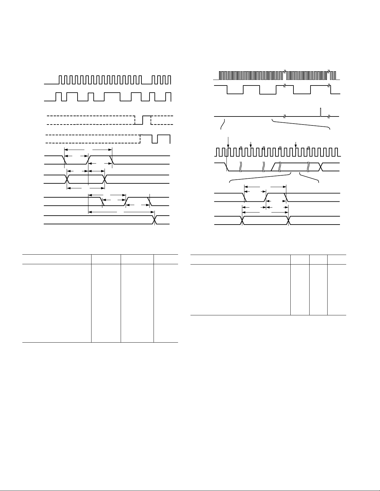
Timing Requirements
(T
A
= –40ⴗC to +85ⴗC, V
CC
= +12 V to +32 V)
THREE-WIRE INTERFACE
CLOCK
DATA IN
LATCH
DATA OUT
CLOCK
DATA IN
LATCH
DATA OUT
WORD "N" WORD "N + 1"
WORD "N – 1"
WORD "N"
1
0 1 1 0 0 1
0 0 1 1 1 0 0 1 1 1
0 0 1
(MSB)
B15
B14
B13
B12
B11
B10
B9
B8
B7
B6
B5
B4
B3
B2
B1
B0
B15
B14
B13
B12
(LSB)
1
01 1
B15
B14
B13
B12
t
CK
t
CL
t
CH
t
DS
t
DH
t
DW
t
LD
t
LL
t
LH
t
SD
Figure 2. Timing Diagram for Three-Wire Interface
Table II. Timing Specification for Three-Wire Interface
Parameter Label Limit Units
Data Clock Period t
CK
300 ns min
Data Clock Low Time t
CL
80 ns min
Data Clock High Time t
CH
80 ns min
Data Stable Width t
DW
125 ns min
Data Setup Time t
DS
40 ns min
Data Hold Time t
DH
5 ns min
Latch Delay Time t
LD
80 ns min
Latch Low Time t
LL
80 ns min
Latch High Time t
LH
80 ns min
Serial Output Delay Time t
SD
225 ns max
Clear Pulsewidth t
CLR
50 ns min
Three-Wire Interface Fast Edges on Digital Input
With a fast rising edge (<10 ns) on one of the serial inputs
(CLOCK, DATA IN, LATCH) while another input is logic
high, the part may be triggered into a test mode and the con-
tents of the data register may become corrupted, which may
result in the output being loaded with an incorrect value. If fast
edges are expected on the digital input lines, it is recommended
that the latch line remain at Logic 0 during serial loading of the
DAC. Similarly, the clock line should remain low during updates
of the DAC via the latch pin. Alternatively, the addition of
small value capacitors on the digital lines will slow down the
edge.
CLOCK
DATA IN
CLOCK
DATA IN
t
ADH
t
ACK
t
ADW
t
ACL
t
ADS
START
BIT
01 100
BIT 15
BIT 14
BITs
13-1
BIT 0
STOP
BIT
NEXT
START
BIT
(INTERNALLY GENERATED LATCH)
EXPANDED TIME VIEW BELOW
CLOCK COUNTER STARTS HERE
CONFIRM START BIT
SAMPLE BIT 15
0 1 2 8 16 24
START BIT
DATA BIT 15
BIT 14
EXPANDED TIME VIEW BELOW
t
ACH
CLOCK
DATA IN
Figure 3. Timing Diagram for Asynchronous Interface
Table III. Timing Specifications for Asynchronous Interface
Parameter Label Limit Units
Asynchronous Clock Period t
ACK
400 ns min
Asynchronous Clock Low Time t
ACL
50 ns min
Asynchronous Clock High Time t
ACH
150 ns min
Data Stable Width (Critical Clock Edge) t
ADW
300 ns min
Data Setup Time (Critical Clock Edge) t
ADS
50 ns min
Data Hold Time (Critical Clock Edge) t
ADH
20 ns min
Clear Pulsewidth t
CLR
50 ns min
ASYNCHRONOUS INTERFACE
Note in the timing diagram for asynchronous mode operation
each data word is “framed” by a START (0) bit and a STOP
(1) bit. The data timing is with respect to the rising edge of the
CLOCK at the center of each bit cell. Bit cells are 16 clocks
long, and the first cell (the START bit) begins at the first clock
following the leading (falling) edge of the START bit. Thus the
MSB (D15) is sampled 24 clock cycles after the beginning of
the START bit, D14 is sampled at clock number 40, and so on.
During any “dead time” before writing the next word the
DATA IN pin must remain at Logic 1.
The DAC output updates when the STOP bit is received. In
the case of a “framing error” (the STOP bit sampled as a 0) the
AD420 will output a pulse at the DATA OUT pin one clock
period wide during the clock period subsequent to sampling the
STOP bit. The DAC output will not update if a “framing error”
is detected.
Loading...