


 Loading...
Variable Resolution, 10-Bit to 16-Bit R/D
Converter with Reference Oscillator
|
|
|
|
|
|
|
|
|
|
|
|
|
|
|
|
|
|
|
|
|
|
|
|
|
|
|
|
|
|
AD2S1210 |
||||||||||
|
|
|
|
|
|
|
|
|
|
|
|
|
|
|
|
|
|
|
|
|
|
|
|
|
|
|
|
|
|
|
|
|
|
|
|
|
|
|
|
|
FEATURES |
|
|
|
|
|
FUNCTIONAL BLOCK DIAGRAM |
|
|
|
|||||||||||||||||||||||||||||||
Complete monolithic resolver-to-digital converter |
|
|
|
|
|
|
|
|
|
|
|
|
|
|
|
|
|
|
|
|
|
REFERENCE |
|
CRYSTAL |
|
|
|
|||||||||||||
|
|
|
|
|
|
|
|
|
|
|
|
|
|
|
|
|
|
|
|
|
|
PINS |
|
|
|
|
||||||||||||||
3125 rps maximum tracking rate (10-bit resolution) |
|
|
|
|
|
|
|
|
|
|
|
|
|
|
|
|
|
|
|
|
|
|
|
|
|
|
|
|
|
|
|
|
|
|
|
|
|
|
|
|
|
|
|
|
|
|
|
|
|
|
|
|
|
|
|
|
|
|
|
|
|
|
|
|
|
|
|
|
|
|
|
|
|
|
|
|
|
|
|
||
±2.5 arc minutes of accuracy |
|
|
|
|
|
|
|
|
|
|
|
|
|
|
|
|
|
|
|
|
|
|
|
|
|
|
|
|
|
|
|
|
|
|
|
|
|
|
|
|
|
|
|
|
|
|
|
|
|
|
|
|
|
|
|
|
|
|
|
|
|
|
|
|
|
|
|
|
|
|
|
|
|
|
|
|
|
|
|
||
10-/12-/14-/16-bit resolution, set by user |
EXCITATION |
|
|
|
|
|
|
REFERENCE |
|
|
VOLTAGE |
|
INTERNAL |
|
|
|
|
|
|
|||||||||||||||||||||
|
|
|
|
|
|
|
|
|
|
CLOCK |
|
|
|
|
|
|
||||||||||||||||||||||||
|
|
OUTPUTS |
|
|
|
|
|
OSCILLATOR |
|
|
REFERENCE |
|
|
|
|
|
|
|
|
|||||||||||||||||||||
Parallel and serial 10-bit to 16-bit data ports |
|
|
|
|
|
|
|
|
(DAC) |
|
|
|
|
|
|
|
|
|
GENERATOR |
|
|
|
|
|
|
|||||||||||||||
|
|
|
|
|
|
|
|
|
|
|
|
|
|
|
|
|
|
|
|
|
|
|
|
|
|
|||||||||||||||
|
|
|
|
|
|
|
|
|
|
|
|
|
|
|
|
|
|
|
|
|||||||||||||||||||||
Absolute position and velocity outputs |
|
|
|
|
|
|
|
|
|
|
|
|
|
|
|
|
|
|
|
|
|
|
|
|
|
|
|
|
|
|
|
|
|
|
|
|
|
|
|
|
|
|
|
|
|
|
|
|
|
|
|
|
|
|
|
|
|
|
|
|
|
|
|
|
|
AD2S1210 |
|
|
|
||||||||||||
|
|
|
|
|
|
|
|
|
|
|
|
|
|
|
|
|
|
|
|
|
|
|
|
|
|
|
|
|||||||||||||
System fault detection |
|
|
|
|
|
|
|
|
|
SYNTHETIC |
|
|
|
|
|
|
|
|
|
|||||||||||||||||||||
Programmable fault detection thresholds |
|
|
|
|
|
|
|
|
|
REFERENCE |
|
|
|
|
|
|
|
|
|
|
|
|
|
|
|
|
|
|
|
|
||||||||||
|
|
|
|
|
|
|
|
|
|
|
|
|
|
|
|
|
|
|
|
|
|
|
|
|
|
|
|
|
|
|
|
|
|
|
|
|
|
|
||
|
|
|
|
|
|
|
|
|
|
|
|
|
|
|
|
|
|
|
|
|
|
|
|
|
|
|
|
|
|
|
|
|
|
|
|
|
|
|
||
Differential inputs |
|
|
|
|
|
|
ADC |
|
|
|
|
|
|
|
|
|
|
|
|
|
|
|
|
|
|
|
|
|
|
|
|
|
|
|
|
|
|
|||
INPUTS |
|
|
|
|
|
|
|
|
|
|
|
|
TYPE II |
|
|
FAULT |
|
|
|
|
FAULT |
|||||||||||||||||||
Incremental encoder emulation |
|
|
|
|
|
|
|
|
|
|
|
|
|
|
|
|
|
|
|
|
|
|||||||||||||||||||
|
|
|
|
|
|
|
|
|
|
|
|
|
|
|
|
|
|
|
|
|
||||||||||||||||||||
FROM |
|
|
|
|
|
|
|
|
|
|
|
|
|
|
|
|
|
|
|
|
DETECTION |
|||||||||||||||||||
|
|
|
|
|
|
|
|
|
|
|
|
|
TRACKING LOOP |
|
DETECTION |
|
|
|
||||||||||||||||||||||
Programmable sinusoidal oscillator on-board |
RESOLVER |
|
|
|
|
|
|
|
|
|
|
|
|
|
|
|
|
|
|
|
|
|
|
|
|
|
|
|
|
|
|
|
|
|
OUTPUTS |
|||||
|
|
|
ADC |
|
|
|
|
|
|
|
|
|
|
|
|
|
|
|
|
|
|
|
|
|
|
|
|
|
|
|
||||||||||
Compatible with DSP and SPI interface standards |
|
|
|
|
|
|
|
|
|
|
|
|
|
|
|
|
|
|
|
|
|
|
|
|
|
|
|
|
|
|
|
|
|
|
|
|
||||
5 V supply with 2.3 V to 5 V logic interface |
|
|
|
|
|
|
|
|
|
|
|
|
|
|
|
|
|
|
|
|
|
|
|
|
|
|
|
|
|
|
|
|
|
|
|
|
|
|
|
|
|
|
|
|
|
|
|
|
|
|
POSITION |
|
|
VELOCITY |
|
CONFIGURATION |
|
|
|
|
|
||||||||||||||||||||
|
|
|
|
|
|
|
|
|
|
|
|
|
|
DATA I/O |
||||||||||||||||||||||||||
−40°C to +125°C temperature rating |
|
|
|
|
|
|
|
|
|
|
REGISTER |
|
|
REGISTER |
|
|
REGISTER |
|
|
|||||||||||||||||||||
|
|
|
|
|
|
|
|
|
|
|
|
|
|
|
||||||||||||||||||||||||||
|
|
|
|
|
|
|
ENCODER EMULATION |
|
|
|
|
|
|
|
|
|
|
|
|
|
|
|
|
|
|
|
|
|
|
|
|
|
|
|
|
|
|
|
||
APPLICATIONS |
ENCODER |
|
|
|
|
|
|
|
|
|
|
|
|
|
|
|
|
|
|
|
|
|
|
|
|
|
|
|
|
|
|
|
|
|
||||||
|
|
|
|
|
|
|
|
MULTIPLEXER |
|
|
|
|
|
|
|
|
|
|
|
|
|
|||||||||||||||||||
EMULATION |
|
|
|
|
|
|
|
|
|
|
|
|
|
|
|
|
|
|
|
|
|
|||||||||||||||||||
DC and ac servo motor control |
OUTPUTS |
|
|
|
|
|
|
|
|
|
|
|
|
|
|
|
|
|
|
|
|
|
|
|
|
|
|
|
|
|
|
|
|
|
||||||
|
|
|
|
|
|
|
|
|
|
|
|
|
|
|
|
|
|
|
|
|
|
|
|
|
|
|
|
|
|
|
|
|
||||||||
|
|
|
|
|
|
|
|
|
|
|
|
|
|
|
|
|
|
|
|
|
|
|
|
|
|
|
|
|
|
|
|
|
|
|
|
|||||
|
|
|
|
|
|
|
|
|
|
|
|
|
|
|
|
|
|
|
|
|
|
|
|
|
|
|
|
|
|
|
|
|
|
|
|
|||||
Encoder emulation |
|
|
|
|
|
|
|
|
|
|
|
|
DATA BUS OUTPUT |
|
|
|
|
|
|
|
|
|
|
|
|
|
||||||||||||||
Electric power steering |
|
|
|
|
|
|
|
|
|
|
|
|
|
|
|
|
|
|
|
|
|
|
|
|
|
|
|
|
|
|
|
|
|
|
|
|
|
|
|
|
|
|
|
|
|
|
|
|
|
|
|
|
|
|
|
|
|
|
|
|
|
|
|
|
|
|
|
|
|
|
|
|
|
|
|
|
|
|
|
||
Electric vehicles |
|
|
|
|
|
|
|
|
|
|
|
|
|
|
|
|
DATA I/O |
|
|
|
|
|
|
|
|
|
|
|
|
-001 |
||||||||||
|
|
|
|
|
|
|
|
|
|
|
|
|
|
|
|
|
|
|
|
|
|
|
|
|
|
|||||||||||||||
|
|
|
|
|
|
|
|
|
|
|
|
|
|
|
|
|
|
|
|
|
|
|
|
|
|
|
|
|||||||||||||
|
|
|
|
|
|
|
|
|
|
|
|
|
|
|
|
|
|
|
|
|
|
|
|
|
|
|
|
|
|
|
|
|
|
|
|
07467 |
||||
|
|
|
|
|
|
RESET |
|
|
|
|
|
|
|
|
|
|
|
|
|
|
|
|
|
|||||||||||||||||
Integrated starter generators/alternators MacshbM
Automotive motion sensing and control |
Figure 1. |
|
GENERAL DESCRIPTION
The AD2S1210 is a complete 10-bit to 16-bit resolution tracking resolver-to-digital converter, integrating an on-board programmable sinusoidal oscillator that provides sine wave excitation for resolvers.
The converter accepts 3.15 V p-p ± 27% input signals, in the range of 2 kHz to 20 kHz on the sine and cosine inputs. A Type II servo loop is employed to track the inputs and convert the input sine and cosine information into a digital representation of the input angle and velocity. The maximum tracking rate is 3125 rps.
Rev. 0
Information furnished by Analog Devices is believed to be accurate and reliable. However, no responsibilityisassumedbyAnalogDevicesforitsuse,norforanyinfringementsofpatentsorother rightsofthirdpartiesthatmayresultfromitsuse.Specificationssubjecttochangewithoutnotice.No license is granted by implication or otherwise under any patent or patent rights of Analog Devices. Trademarksandregisteredtrademarksarethepropertyoftheirrespectiveowners.
PRODUCT HIGHLIGHTS
1.Ratiometric tracking conversion. The Type II tracking loop provides continuous output position data without conversion delay. It also provides noise immunity and tolerance of harmonic distortion on the reference and input signals.
2.System fault detection. A fault detection circuit can sense loss of resolver signals, out-of-range input signals, input signal mismatch, or loss of position tracking. The fault detection threshold levels can be individually programmed by the user for optimization within a particular application.
3.Input signal range. The sine and cosine inputs can accept differential input voltages of 3.15 V p-p ± 27%.
4.Programmable excitation frequency. Excitation frequency is easily programmable to a number of standard frequencies between 2 kHz and 20 kHz.
5.Triple format position data. Absolute 10-bit to 16-bit angular position data is accessed via either a 16-bit parallel port or a 4-wire serial interface. Incremental encoder emulation is in standard A-quad-B format with direction output available.
6.Digital velocity output. 10-bit to 16-bit signed digital velocity accessed via either a 16-bit parallel port or a 4-wire serial interface.
One Technology Way, P.O. Box 9106, Norwood, MA 02062-9106, U.S.A.
Tel: 781.329.4700 |
www.analog.com |
Fax: 781.461.3113 |
©2008 Analog Devices, Inc. All rights reserved. |

AD2S1210
TABLE OF CONTENTS
Features .............................................................................................. |
|
|
1 |
|
LOS Threshold Register ............................................................ |
21 |
||
Applications....................................................................................... |
|
1 |
|
DOS Overrange Threshold Register........................................ |
21 |
|||
Functional Block Diagram .............................................................. |
1 |
|
DOS Mismatch Threshold Register......................................... |
21 |
||||
General Description ......................................................................... |
1 |
|
DOS Reset Maximum and Minimum Threshold Registers . 22 |
|||||
Product Highlights ........................................................................... |
1 |
|
LOT High Threshold Register .................................................. |
22 |
||||
Revision History ............................................................................... |
2 |
|
LOT Low Threshold Register ................................................... |
22 |
||||
Specifications..................................................................................... |
|
3 |
|
Excitation Frequency Register.................................................. |
22 |
|||
Timing Specifications .................................................................. |
6 |
|
Control Register ......................................................................... |
22 |
||||
Absolute Maximum Ratings............................................................ |
8 |
|
Software Reset Register ............................................................. |
23 |
||||
ESD Caution.................................................................................. |
8 |
|
Fault Register .............................................................................. |
23 |
||||
Pin Configuration and Function Descriptions............................. |
9 |
Digital interface .............................................................................. |
24 |
|||||
Typical Performance Characteristics |
11 |
|
|
|
24 |
|||
|
SOE |
....................................................................................Input |
||||||
Resolver Format Signals |
15 |
|
|
24 |
||||
|
SAMPLE |
............................................................................Input |
||||||
Theory of Operation ...................................................................... |
16 |
|
Data Format ................................................................................ |
24 |
||||
Resolver to Digital Conversion................................................. |
16 |
|
Parallel Interface......................................................................... |
24 |
||||
Fault Detection Circuit .............................................................. |
16 |
|
Serial Interface ............................................................................ |
28 |
||||
On-Board Programmable Sinusoidal Oscillator .................... |
18 |
|
Incremental Encoder Outputs.................................................. |
31 |
||||
Modes of |
|
MacshbMLoop Response Model ............................................................... 32 |
||||||
Synthetic Reference Generation ............................................... |
18 |
|
Supply Sequen ing and Re et ................................................... |
31 |
||||
Configuration of AD2S1210 ......................................................... |
20 |
Circuit Dynami ........................................................................... |
32 |
|||||
|
Operation ................................................................... |
20 |
|
|
|
|
|
|
Register Map.................................................................................... |
|
21 |
|
Sources of Error.......................................................................... |
33 |
|||
Position Register......................................................................... |
21 |
Outline Dimensions ....................................................................... |
34 |
|||||
Velocity Register ......................................................................... |
21 |
|
Ordering Guide .......................................................................... |
34 |
||||
REVISION HISTORY
8/08—Revision 0: Initial Version
Rev. 0 | Page 2 of 36

AD2S1210
SPECIFICATIONS
AVDD = DVDD = 5.0 V ± 5%, CLKIN = 8.192 MHz ± 25%, EXC, EXC frequency = 10 kHz to 20 kHz (10-bit); 6 kHz to 20 kHz (12-bit); 3 kHz to 12 kHz (14-bit); 2 kHz to 10 kHz (16-bit); TA = TMIN to TMAX; unless otherwise noted.1
Table 1.
Parameter |
Min |
Typ |
Max |
Unit |
Conditions/Comments |
|
|
|
|
|
|
SINE, COSINE INPUTS2 |
|
|
|
|
|
Voltage Amplitude |
2.3 |
3.15 |
4.0 |
V p-p |
Sinusoidal waveforms, differential SIN to SINLO, |
|
|
|
|
|
COS to COSLO |
Input Bias Current |
|
|
8.25 |
μA |
VIN = 4.0 V p-p, CLKIN = 8.192 MHz |
Input Impedance |
485 |
|
|
kΩ |
VIN = 4.0 V p-p, CLKIN = 8.192 MHz |
Phase Lock Range |
−44 |
|
+44 |
Degrees |
Sine/cosine vs. EXC output, Control Register D3 = 0 |
Common-Mode Rejection |
|
±20 |
|
arc sec/V |
10 Hz to 1 MHz, Control Register D4 = 0 |
ANGULAR ACCURACY3 |
|
|
|
|
|
Angular Accuracy |
|
±2.5 + 1 LSB |
±5 + 1 LSB |
arc min |
B, D grades |
|
|
±5 + 1 LSB |
±10 + 1 LSB |
arc min |
A, C grades |
Resolution |
|
10, 12, 14, 16 |
|
Bits |
No missing codes |
Linearity INL |
|
|
|
|
|
10-bit |
|
|
±1 |
LSB |
B, D grades |
|
|
|
±2 |
LSB |
A, C grades |
12-bit |
|
|
±2 |
LSB |
B, D grades |
|
|
|
±4 |
LSB |
A, C grades |
14-bit |
|
|
±4 |
LSB |
B, D grades |
|
|
|
±8 |
LSB |
A, C grades |
16-bit |
|
|
±16 |
LSB |
B, D grades |
|
|
|
±32 |
LSB |
A, C grades |
Linearity DNL |
|
|
±0.9 |
LSB |
shbM |
Repeatability |
|
±1 |
|
LSB |
|
Mac |
|||||
VELOCITY OUTPUT |
|
|
|
|
|
Velocity Accuracy4 |
|
|
|
|
|
10-bit |
|
|
±2 |
LSB |
B, D grades, zero acceleration |
|
|
|
±4 |
LSB |
A, C grades, zero acceleration |
12-bit |
|
|
±2 |
LSB |
B, D grades, zero acceleration |
|
|
|
±4 |
LSB |
A, C grades, zero acceleration |
14-bit |
|
|
±4 |
LSB |
B, D grades, zero acceleration |
|
|
|
±8 |
LSB |
A, C grades, zero acceleration |
16-bit |
|
|
±16 |
LSB |
B, D grades, zero acceleration |
|
|
|
±32 |
LSB |
A, C grades, zero acceleration |
Resolution5 |
|
9, 11, 13, 15 |
|
Bits |
|
DYNAMNIC PERFORMANCE |
|
|
|
|
|
Bandwidth |
|
|
|
|
|
10-bit |
2000 |
|
6500 |
Hz |
|
|
2900 |
|
5300 |
Hz |
CLKIN = 8.192 MHz |
12-bit |
900 |
|
2800 |
Hz |
|
|
1200 |
|
2200 |
Hz |
CLKIN = 8.192 MHz |
14-bit |
400 |
|
1500 |
Hz |
|
|
600 |
|
1200 |
Hz |
CLKIN = 8.192 MHz |
16-bit |
100 |
|
350 |
Hz |
|
|
125 |
|
275 |
Hz |
CLKIN = 8.192 MHz |
|
|
|
|
|
|
Rev. 0 | Page 3 of 36

AD2S1210
Parameter |
|
Min |
Typ |
Max |
Unit |
Conditions/Comments |
||||||||||||
|
|
|
|
|
|
|
|
|
|
|
|
|
|
|
|
|
|
|
Tracking Rate |
|
|
|
|
|
|
|
|
|
|
|
|
|
|
||||
|
10-bit |
|
|
|
3125 |
rps |
CLKIN = 10.24 MHz |
|||||||||||
|
|
|
|
|
|
|
|
2500 |
|
CLKIN = 8.192 MHz |
||||||||
|
12-bit |
|
|
|
1250 |
rps |
CLKIN = 10.24 MHz |
|||||||||||
|
|
|
|
|
|
|
|
1000 |
|
CLKIN = 8.192 MHz |
||||||||
|
14-bit |
|
|
|
625 |
rps |
CLKIN = 10.24 MHz |
|||||||||||
|
|
|
|
|
|
|
|
500 |
|
CLKIN = 8.192 MHz |
||||||||
|
16-bit |
|
|
|
156.25 |
rps |
CLKIN = 10.24 MHz |
|||||||||||
|
|
|
|
|
|
|
|
125 |
|
CLKIN = 8.192 MHz |
||||||||
Acceleration Error |
|
|
|
|
|
|
|
|
|
|
|
|
|
|||||
|
10-bit |
|
|
30 |
|
arc min |
At 50,000 rps2, CLKIN = 8.192 MHz |
|||||||||||
|
12-bit |
|
|
30 |
|
arc min |
At 10,000 rps2, CLKIN = 8.192 MHz |
|||||||||||
|
14-bit |
|
|
30 |
|
arc min |
At 2500 rps2, CLKIN = 8.192 MHz |
|||||||||||
|
16-bit |
|
|
30 |
|
arc min |
At 125 rps2, CLKIN = 8.192 MHz |
|||||||||||
Settling Time 10° Step Input |
|
|
|
|
|
|
|
|
|
|
|
|
|
|||||
|
10-bit |
|
|
0.6 |
0.9 |
ms |
To settle to within ±2 LSB , CLKIN = 8.192 MHz |
|||||||||||
|
12-bit |
|
|
2.2 |
3.1 |
ms |
To settle to within ±2 LSB, CLKIN = 8.192 MHz |
|||||||||||
|
14-bit |
|
|
6.5 |
9.0 |
ms |
To settle to within ±2 LSB , CLKIN = 8.192 MHz |
|||||||||||
|
16-bit |
|
|
27.5 |
40 |
ms |
To settle to within ±2 LSB, CLKIN = 8.192 MHz |
|||||||||||
Settling Time 179° Step Input |
|
|
|
|
|
|
|
|
|
|
|
|
|
|||||
|
10-bit |
|
|
1.5 |
2.2 |
ms |
To settle to within ±2 LSB , CLKIN = 8.192 MHz |
|||||||||||
|
12-bit |
|
|
4.75 |
6.0 |
ms |
To settle to within ±2 LSB, CLKIN = 8.192 MHz |
|||||||||||
|
14-bit |
|
|
10.5 |
14.7 |
ms |
To settle to within ±2 LSB , CLKIN = 8.192 MHz |
|||||||||||
|
16-bit |
|
|
45 |
66 |
ms |
To settle to within ±2 LSB, CLKIN = 8.192 MHz |
|||||||||||
|
|
|
|
|
|
|
|
|
|
|
|
|
|
|
|
|||
EXC, |
|
|
OUTPUTS |
|
|
|
|
|
|
|
|
|
|
|
|
|
||
EXC |
|
|
|
|
|
|
|
|
|
|
|
|
|
|||||
Voltage |
|
3.2 |
3.6 |
4.0 |
V p-p |
Load ±100 μA, typical differential output |
||||||||||||
|
|
|
|
|
|
|
|
|
|
(EXC to EXC) = 7.2 V p-p |
||||||||
Center Voltage |
2.40 |
2.47 |
2.53 |
V |
shbM |
|||||||||||||
|
|
|
|
|
Mac |
|||||||||||||
Frequency |
|
2 |
|
20 |
kHz |
|
|
|
|
|
|
|
|
|
||||
|
|
DC Mismatch |
|
|
30 |
mV |
|
|
|
|
|
|
|
|
|
|||
EXC/EXC |
|
|
|
|
|
|
|
|
|
|
|
|||||||
|
|
|
|
|
100 |
mV |
|
|
|
|
|
|
|
|
|
|||
EXC/EXC |
AC Mismatch |
|
|
|
|
|
|
|
|
|
|
|
||||||
THD |
|
|
−58 |
|
dB |
First five harmonics |
||||||||||||
VOLTAGE REFERENCE |
|
|
|
|
|
|
|
|
|
|
|
|
|
|||||
REFOUT |
|
2.40 |
2.47 |
2.53 |
V |
±IOUT = 100 μA |
||||||||||||
Drift |
|
|
100 |
|
ppm/°C |
|
|
|
|
|
|
|
|
|
||||
PSRR |
|
|
−60 |
|
dB |
|
|
|
|
|
|
|
|
|
||||
|
|
|
|
|
|
|
|
|
|
|
|
|
|
|||||
CLKIN, XTALOUT6 |
|
|
|
|
|
|
|
|
|
|
|
|
|
|||||
VIL Voltage Input Low |
|
|
0.8 |
V |
|
|
|
|
|
|
|
|
|
|||||
VIH Voltage Input High |
2.0 |
|
|
V |
|
|
|
|
|
|
|
|
|
|||||
|
|
|
|
|
|
|
|
|
|
|
|
|
|
|
||||
LOGIC INPUTS |
|
|
|
|
|
|
|
|
|
|
|
|
|
|
||||
VIL Voltage Input Low |
|
|
0.8 |
V |
VDRIVE = 2.7 V to 5.25 V |
|||||||||||||
|
|
|
|
|
|
|
|
0.7 |
V |
VDRIVE = 2.3 V to 2.7 V |
||||||||
VIH Voltage Input High |
2.0 |
|
|
V |
VDRIVE = 2.7 V to 5.25 V |
|||||||||||||
|
|
|
|
|
|
1.7 |
|
|
V |
VDRIVE = 2.3 V to 2.7 V |
||||||||
IIL Low Level Input Current (Non |
|
|
10 |
μA |
|
|
|
|
|
|
|
|
|
|||||
|
Pull-Up) |
|
|
|
|
|
|
|
|
|
|
|
|
|
|
|||
IIL Low Level Input Current (Pull-Up) |
|
|
80 |
μA |
|
|
|
|
|
|
|
|
|
|||||
|
|
RES0, RES1, |
RD, |
|
WR/FSYNC, A0, A1, and RESET pins |
|||||||||||||
IIH High Level Input Current |
−10 |
|
|
μA |
|
|
|
|
|
|
|
|
|
|||||
LOGIC OUTPUTS |
|
|
|
|
|
|
|
|
|
|
|
|
|
|||||
VOL Voltage Output Low |
|
|
0.4 |
V |
VDRIVE = 2.3 V to 5.25 V |
|||||||||||||
VOH Voltage Output High |
2.4 |
|
|
V |
VDRIVE = 2.7 V to 5.25 V |
|||||||||||||
|
|
|
|
|
|
2.0 |
|
|
V |
VDRIVE = 2.3 V to 2.7 V |
||||||||
IOZH High Level Three-State Leakage |
−10 |
|
|
μA |
|
|
|
|
|
|
|
|
|
|||||
IOZL Low Level Three-State Leakage |
|
|
10 |
μA |
|
|
|
|
|
|
|
|
|
|||||
|
|
|
|
|
|
|
|
|
|
|
|
|
|
|
|
|
|
|
Rev. 0 | Page 4 of 36

AD2S1210
Parameter |
Min |
Typ |
Max |
Unit |
Conditions/Comments |
|
|
|
|
|
|
POWER REQUIREMENTS |
|
|
|
|
|
AVDD |
4.75 |
|
5.25 |
V |
|
DVDD |
4.75 |
|
5.25 |
V |
|
VDRIVE |
2.3 |
|
5.25 |
V |
|
POWER SUPPLY |
|
|
|
|
|
IAVDD |
|
|
12 |
mA |
|
IDVDD |
|
|
35 |
mA |
|
IOVDD |
|
|
2 |
mA |
|
|
|
|
|
|
|
1 Temperature ranges are as follows: A, B grades: –40°C to +85°C; C, D grades: –40°C to +125°C.
2 The voltages, SIN, SINLO, COS, and COSLO, relative to AGND, must always be between 0.15 V and AVDD − 0.2 V.
3 All specifications within the angular accuracy parameter are tested at constant velocity, that is, zero acceleration. 4 The velocity accuracy specification includes velocity offset and dynamic ripple.
5For example when RES0 = 0 and RES1 = 1, the position output has a resolution of 12 bits. The velocity output has a resolution of 11 bits with the MSB indicating the direction of rotation. In this example, with a CLKIN frequency of 8.192 MHz the velocity LSB is 0.488 rps, that is, 1000 rps/(211).
6The clock frequency of the AD2S1210 can be supplied with a crystal, an oscillator, or directly from a DSP/microprocessor digital output. When using a single-ended clock signal directly from the DSP/microprocessor, the XTALOUT pin should remain open circuit and the logic levels outlined under the logic inputs parameter in Table 1 apply.
MacshbM
Rev. 0 | Page 5 of 36

AD2S1210
TIMING SPECIFICATIONS
AVDD = DVDD = 5.0 V ± 5%, TA = TMIN to TMAX, unless otherwise noted.1
Table 2.
Parameter |
|
|
Description |
|
Limit at TMIN, TMAX |
Unit |
|
|||||||||||||||||||||||||||||||||||||||||||||||||||||||
|
|
|
|
|
|
|
|
|
|
|
|
|
|
|
|
|
|
|
|
|
|
|
|
|
|
|
|
|
|
|
|
|
|
|
|
|
|
|
|
|
|
|
|
|
|
|
|
|
|
|
|
|
|
|
|
|
|
|
|
|
|
|
fCLKIN |
|
|
Frequency of clock input |
6.144 |
MHz min |
|||||||||||||||||||||||||||||||||||||||||||||||||||||||||
|
|
|
|
|
|
|
|
|
|
|
|
|
|
|
|
|
|
|
|
|
|
|
|
|
|
|
|
|
|
|
|
|
|
|
|
|
|
|
|
|
|
|
|
|
|
|
|
|
|
|
|
|
|
|
|
|
|
|
|
10.24 |
MHz max |
|
tCK |
|
|
Clock period ( = 1/fCLKIN) |
|
98 |
ns min |
||||||||||||||||||||||||||||||||||||||||||||||||||||||||
|
|
|
|
|
|
|
|
|
|
|
|
|
|
|
|
|
|
|
|
|
|
|
|
|
|
|
|
|
|
|
|
|
|
|
|
|
|
|
|
|
|
|
|
|
|
|
|
|
|
|
|
|
|
|
|
|
|
|
|
163 |
ns max |
|
t1 |
|
|
|
|
|
|
|
|
|
|
|
|
|
|
|
|
|
|
|
|
|
|
|
|
|
|
|
|
|
|
|
|
|
|
|
|
|
|
|
|
|
|
|
|
|
|
|
|
|
|
|
|
|
|
|
|
|
|
|
2 |
ns min |
|
|
|
A0 and A1 setup time before |
RD/CS low |
|
||||||||||||||||||||||||||||||||||||||||||||||||||||||||||
t2 |
|
|
|
|
|
|
|
|
|
|
|
|
|
|
|
|
|
|
|
|
|
|
|
|
|
|
|
|
|
|
|
|
|
|
|
|
|
|
|
|
|
|
|
|
|
|
|
|
|
|
|
|
|
|
|
|
22 |
ns min |
||||
|
|
Delay |
CS |
falling edge to |
WR/FSYNC rising edge |
|
||||||||||||||||||||||||||||||||||||||||||||||||||||||||
t3 |
|
|
Address/data setup time during a write cycle |
|
3 |
ns min |
||||||||||||||||||||||||||||||||||||||||||||||||||||||||
t4 |
|
|
Address/data hold time during a write cycle |
|
2 |
ns min |
||||||||||||||||||||||||||||||||||||||||||||||||||||||||
t5 |
|
|
|
|
|
|
|
|
|
|
|
|
|
|
|
|
|
|
|
|
|
|
|
|
|
|
|
|
|
|
|
|
|
|
|
|
|
|
|
|
|
|
|
|
|
|
|
|
|
|
2 |
ns min |
||||||||||
|
|
Delay |
WR/FSYNC rising edge to CS rising edge |
|
||||||||||||||||||||||||||||||||||||||||||||||||||||||||||
t6 |
|
|
|
|
|
|
|
|
|
|
|
|
|
|
|
|
|
|
|
|
|
|
|
falling edge |
|
10 |
ns min |
|||||||||||||||||||||||||||||||||||
|
|
Delay |
CS |
rising edge to |
CS |
|
||||||||||||||||||||||||||||||||||||||||||||||||||||||||
t7 |
|
|
Delay between writing address and writing data |
|
2 × tCK + 20 |
ns min |
||||||||||||||||||||||||||||||||||||||||||||||||||||||||
t8 |
|
|
|
|
|
|
|
|
|
|
|
|
|
|
|
|
|
|
|
|
|
|
|
|
|
|
|
|
|
|
|
|
|
|
|
|
|
|
|
|
|
|
|
2 |
ns min |
|||||||||||||||||
|
|
A0 and A1 hold time after |
WR/FSYNC rising edge |
|
||||||||||||||||||||||||||||||||||||||||||||||||||||||||||
t9 |
|
|
Delay between successive write cycles |
|
6 × tCK + 20 |
ns min |
||||||||||||||||||||||||||||||||||||||||||||||||||||||||
t10 |
|
|
|
|
|
|
|
|
|
|
|
|
|
|
|
|
|
|
|
|
|
|
|
|
|
|
|
|
|
|
|
|
|
|
|
|
|
|
|
|
2 |
ns min |
||||||||||||||||||||
|
|
Delay between rising edge of |
WR/FSYNC and falling edge of RD |
|
||||||||||||||||||||||||||||||||||||||||||||||||||||||||||
t11 |
|
|
|
|
|
|
|
|
|
|
|
|
|
|
|
|
|
|
|
|
|
|
|
|
|
|
|
|
|
|
|
|
|
|
2 |
ns min |
||||||||||||||||||||||||||
|
|
Delay |
CS |
falling edge to |
RD |
|
falling edge |
|
||||||||||||||||||||||||||||||||||||||||||||||||||||||
t12 |
|
|
|
|
|
|
|
|
|
|
low to data valid in configuration mode |
|
|
|
|
|||||||||||||||||||||||||||||||||||||||||||||||
|
|
Enable delay |
RD |
|
|
|
|
|
||||||||||||||||||||||||||||||||||||||||||||||||||||||
|
|
|
|
VDRIVE = 4.5 V to 5.25 V |
|
37 |
ns min |
|||||||||||||||||||||||||||||||||||||||||||||||||||||||
|
|
|
|
VDRIVE = 2.7 V to 3.6 V |
|
25 |
ns min |
|||||||||||||||||||||||||||||||||||||||||||||||||||||||
|
|
|
|
VDRIVE = 2.3 V to 2.7 V |
|
30 |
ns min |
|||||||||||||||||||||||||||||||||||||||||||||||||||||||
t14B |
|
|
|
|
|
|
|
|
|
|
|
|
|
|
|
|
|
|
|
|
|
|
|
|
|
|
|
|
|
|
|
|
|
|||||||||||||||||||||||||||||
Disable delay CS high to data highMacshbM-Z 16 ns min |
||||||||||||||||||||||||||||||||||||||||||||||||||||||||||||||
t13 |
|
|
RD rising edge to CS rising edge |
2 |
ns min |
|||||||||||||||||||||||||||||||||||||||||||||||||||||||||
t14A |
|
|
Disable delay |
RD |
|
high to data high-Z |
16 |
ns min |
||||||||||||||||||||||||||||||||||||||||||||||||||||||
t15 |
|
|
|
|
|
|
|
|
|
|
|
|
|
|
|
|
|
|
|
|
|
|
|
|
|
|
|
|
2 |
ns min |
||||||||||||||||||||||||||||||||
|
|
Delay between rising edge of |
RD |
and falling edge of |
WR/FSYNC |
|||||||||||||||||||||||||||||||||||||||||||||||||||||||||
t16 |
|
|
|
|
|
|
|
|
|
|
|
|
|
|
|
|
|
|
|
|
|
|
2 × tCK + 20 |
ns min |
||||||||||||||||||||||||||||||||||||||
|
|
SAMPLE |
pulse width |
|
||||||||||||||||||||||||||||||||||||||||||||||||||||||||||
t17 |
|
|
|
|
|
|
|
|
|
|
|
|
|
|
|
|
|
|
|
|
|
|
6 × tCK + 20 |
ns min |
||||||||||||||||||||||||||||||||||||||
|
|
Delay from |
SAMPLE |
before |
RD/CS low |
|
||||||||||||||||||||||||||||||||||||||||||||||||||||||||
t18 |
|
|
|
|
|
|
|
|
low |
2 |
ns min |
|||||||||||||||||||||||||||||||||||||||||||||||||||
|
|
Hold time |
RD |
before |
RD |
|||||||||||||||||||||||||||||||||||||||||||||||||||||||||
t19 |
|
|
|
|
|
|
|
|
|
|
|
|
|
|
|
|
|
|||||||||||||||||||||||||||||||||||||||||||||
|
|
Enable delay |
RD/CS low to data valid |
|
|
|
|
|||||||||||||||||||||||||||||||||||||||||||||||||||||||
|
|
|
|
VDRIVE = 4.5 V to 5.25 V |
17 |
ns min |
||||||||||||||||||||||||||||||||||||||||||||||||||||||||
|
|
|
|
VDRIVE = 2.7 V to 3.6 V |
21 |
ns min |
||||||||||||||||||||||||||||||||||||||||||||||||||||||||
|
|
|
|
VDRIVE = 2.3 V to 2.7 V |
33 |
ns min |
||||||||||||||||||||||||||||||||||||||||||||||||||||||||
t20 |
|
|
|
|
|
|
|
|
6 |
ns min |
||||||||||||||||||||||||||||||||||||||||||||||||||||
|
|
RD |
pulse width |
|||||||||||||||||||||||||||||||||||||||||||||||||||||||||||
t21 |
|
|
|
|
|
|
|
|
|
|
|
|
||||||||||||||||||||||||||||||||||||||||||||||||||
|
|
A0 and A1 set time to data valid when |
RD/CS low |
|
|
|
|
|||||||||||||||||||||||||||||||||||||||||||||||||||||||
|
|
|
|
VDRIVE = 4.5 V to 5.25 V |
36 |
ns min |
||||||||||||||||||||||||||||||||||||||||||||||||||||||||
|
|
|
|
VDRIVE = 2.7 V to 3.6 V |
37 |
ns min |
||||||||||||||||||||||||||||||||||||||||||||||||||||||||
|
|
|
|
VDRIVE = 2.3 V to 2.7 V |
29 |
ns min |
||||||||||||||||||||||||||||||||||||||||||||||||||||||||
t22 |
|
|
|
|
|
|
|
3 |
ns min |
|||||||||||||||||||||||||||||||||||||||||||||||||||||
|
|
Delay |
WR/FSYNC falling edge to SCLK rising edge |
|||||||||||||||||||||||||||||||||||||||||||||||||||||||||||
t23 |
|
|
|
|
|
|
|
|
|
|
|
|||||||||||||||||||||||||||||||||||||||||||||||||||
|
|
Delay |
WR/FSYNC falling edge to SDO release from high-Z |
|
|
|
|
|||||||||||||||||||||||||||||||||||||||||||||||||||||||
|
|
|
|
VDRIVE = 4.5 V to 5.25 V |
16 |
ns min |
||||||||||||||||||||||||||||||||||||||||||||||||||||||||
|
|
|
|
VDRIVE = 2.7 V to 3.6 V |
26 |
ns min |
||||||||||||||||||||||||||||||||||||||||||||||||||||||||
|
|
|
|
VDRIVE = 2.3 V to 2.7 V |
29 |
ns min |
||||||||||||||||||||||||||||||||||||||||||||||||||||||||
t24 |
|
|
Delay SCLK rising edge to DBx valid |
|
|
|
|
|||||||||||||||||||||||||||||||||||||||||||||||||||||||
|
|
|
|
VDRIVE = 4.5 V to 5.25 V |
24 |
ns min |
||||||||||||||||||||||||||||||||||||||||||||||||||||||||
|
|
|
|
VDRIVE = 2.7 V to 3.6 V |
18 |
ns min |
||||||||||||||||||||||||||||||||||||||||||||||||||||||||
|
|
|
|
VDRIVE = 2.3 V to 2.7 V |
32 |
ns min |
||||||||||||||||||||||||||||||||||||||||||||||||||||||||
t25 |
|
|
SCLK high time |
|
0.4 × tCK |
ns min |
||||||||||||||||||||||||||||||||||||||||||||||||||||||||
t26 |
|
|
SCLK low time |
|
0.4 × tCK |
ns min |
||||||||||||||||||||||||||||||||||||||||||||||||||||||||
t27 |
|
|
SDI setup time prior to SCLK falling edge |
3 |
ns min |
|||||||||||||||||||||||||||||||||||||||||||||||||||||||||
t28 |
|
|
SDI hold time after SCLK falling edge |
|
2 |
ns min |
|
|||||||||||||||||||||||||||||||||||||||||||||||||||||||
Rev. 0 | Page 6 of 36

|
|
|
|
|
|
|
|
|
|
|
|
|
|
|
|
|
|
|
|
|
|
|
|
|
|
|
|
|
|
|
|
AD2S1210 |
|
|
|
|
|
|
|
|
|
|
|
|
|
|
|
|
|
|
|
|
|
|
|
|
|
|
|
|
|
|
|
|
|
|
|
|
|
|
|
|
|
|
|
|
|
|
|
|
|
|
|
|
|
|
|
|
|
|
|
|
|
|
|
|
|
|
Parameter |
Description |
Limit at TMIN, TMAX |
Unit |
|||||||||||||||||||||||||||||
t29 |
Delay |
WR/FSYNC rising edge to SDO high-Z |
15 |
ns min |
||||||||||||||||||||||||||||
t30 |
|
|
|
|
|
|
|
|
|
|
|
|
|
|
|
|
|
|
|
|
|
|
|
|
|
|
6 × tCK + 20 ns |
ns min |
||||
Delay from |
SAMPLE |
before |
WR/FSYNC falling edge |
|||||||||||||||||||||||||||||
t31 |
|
|
|
|
|
|
|
|
|
|
|
|
|
|
|
|
|
|
|
|
2 |
ns min |
||||||||||
Delay |
CS |
falling edge to |
WR/FSYNC falling edge in normal mode |
|||||||||||||||||||||||||||||
t32 |
|
|
|
|
|
|
|
|
|
|
|
|
|
|
|
2 |
ns min |
|||||||||||||||
A0 and A1 setup time before |
WR/FSYNC falling edge |
|||||||||||||||||||||||||||||||
t33 |
|
|
|
|
|
|
|
|
|
|
|
|
|
|||||||||||||||||||
A0 and A1 hold time after |
WR/FSYNC falling edge2 |
|
|
|||||||||||||||||||||||||||||
|
In normal mode, A0 = 0, A1 = 0/1 |
24 × tCK + 5 ns |
ns min |
|||||||||||||||||||||||||||||
|
In configuration mode, A0 = 1, A1 = 1 |
8 × tCK + 5 ns |
ns min |
|||||||||||||||||||||||||||||
t34 |
|
|
|
|
|
|
|
|
|
|
10 |
ns min |
||||||||||||||||||||
Delay |
WR/FSYNC rising edge to WR/FSYNC falling edge |
|||||||||||||||||||||||||||||||
fSCLK |
Frequency of SCLK input |
|
|
|||||||||||||||||||||||||||||
|
VDRIVE = 4.5 V to 5.25 V |
20 |
MHz |
|||||||||||||||||||||||||||||
|
VDRIVE = 2.7 V to 3.6 V |
25 |
MHz |
|||||||||||||||||||||||||||||
|
VDRIVE = 2.3 V to 2.7 V |
15 |
MHz |
|||||||||||||||||||||||||||||
|
|
|
|
|
|
|
|
|
|
|
|
|
|
|
|
|
|
|
|
|
|
|
|
|
|
|
|
|
|
|
|
|
1 Temperature ranges are as follows: A, B grades: –40°C to +85°C; C, D grades: –40°C to +125°C.
2A0 and A1 should remain constant for the duration of the serial readback. This may require 24 clock periods to read back the 8-bit fault information in addition to the 16 bits of position/velocity data. If the fault information is not required, A0/A1 may be released following 16 clock cycles.
MacshbM
Rev. 0 | Page 7 of 36

AD2S1210
ABSOLUTE MAXIMUM RATINGS
Table 3.
Parameter |
Rating |
|
|
AVDD to AGND, DGND |
−0.3 V to +7.0 V |
DVDD to AGND, DGND |
−0.3 V to +7.0 V |
VDRIVE to AGND, DGND |
−0.3 V to AVDD |
AVDD to DVDD |
−0.3 V to +0.3 V |
AGND to DGND |
−0.3 V to +0.3 V |
Analog Input Voltage to AGND |
−0.3 V to AVDD + 0.3 V |
Digital Input Voltage to DGND |
−0.3 V to VDRIVE + 0.3 V |
Digital Output Voltage to DGND |
−0.3 V to VDRIVE + 0.3 V |
Analog Output Voltage Swing |
−0.3 V to AVDD + 0.3 V |
Input Current to Any Pin Except Supplies1 |
±10 mA |
Operating Temperature Range (Ambient) |
|
A, B Grades |
−40°C to +85°C |
C, D Grades |
−40°C to +125°C |
Storage Temperature Range |
−65°C to +150°C |
θJA Thermal Impedance2 |
54°C/W |
θJA Thermal Impedance2 |
15°C/W |
RoHS-Compliant Temperature, Soldering |
260(−5/+0)oC |
Reflow |
|
ESD |
2 kV HBM |
Stresses above those listed under Absolute Maximum Ratings may cause permanent damage to the device. This is a stress rating only; functional operation of the device at these or any other conditions above those indicated in the operational section of this specification is not implied. Exposure to absolute maximum rating conditions for extended periods may affect device reliability.
ESD CAUTION
1 Transient currents of up to 100 mA do not cause latch-up.
2 JEDEC 2S2P standard board.
MacshbM
Rev. 0 | Page 8 of 36
AD2S1210
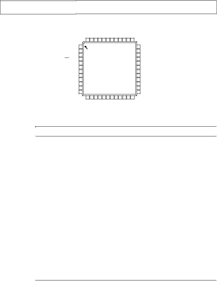
PIN CONFIGURATION AND FUNCTION DESCRIPTIONS
|
|
|
|
|
|
|
|
|
|
|
|
|
|
|
|
|
|
|
|
|
|
|
|
|
|
|
|
|
|
|
|
|
|
|
|
|
|
|
RES0 |
|
REFOUT |
REFBYP |
COS |
COSLO |
|
DD |
SINLO |
SIN |
AGND |
|
EXC |
EXC |
|
|
|
|
|
|
|
|
|
|
|
|
|
|
|
|
|
|
|
|
|
|||||
|
|
|
|
|
|
|
|
|
|
|
|
|
|
|
|
|
|
|
|
|
|
|
|
|
|
|
|
|
|
|
|
|
|
|
|
|
|
|
|
|
|
|
|
|
|
|
|
|
|
|
|
|
|
|
|
|
|
|
|
|
|
|||||||||||||||||
|
|
|
|
|
|
|
|
|
|
|
|
|
|
|
|
|
|
|
|
|
|
|
|
|
|
|
|
|
|
|
|
|
|
|
|
|
|
|
|
AV |
|
A0 |
|
|
|
|
|
|
|
|
|
|
|
|
|
|
|
|
|
|
|
|
||||||||||||||||
|
|
|
|
|
|
|
|
|
|
|
|
|
|
|
|
|
|
|
|
|
|
|
|
|
|
|
|
|
|
|
|
|
|
|
|
|
|
|
|
|
|
|
|
|
|
|
|
|
|
|
|
|
|
|
|
|||||||||||||||||||||||
|
|
|
|
|
|
|
|
|
|
|
|
|
|
|
|
|
|
|
|
|
|
|
|
|
|
|
|
|
|
|
|
|
|
|
48 |
47 |
46 |
45 |
|
44 |
43 |
42 |
41 |
40 |
39 |
38 |
37 |
|
|
|
|
|
|
|
|
|
|
|
|
|
|
|
|
|
|
|
|
|||||||||||
|
|
|
|
|
|
|
|
|
|
|
|
|
|
|
|
|
|
|
|
|
|
|
|
|
|
RES1 |
1 |
|
|
|
|
PIN 1 |
|
|
|
|
|
|
|
|
|
|
|
|
36 |
A1 |
||||||||||||||||||||||||||||||||
|
|
|
|
|
|
|
|
|
|
|
|
|
|
|
|
|
|
|
|
|
|
|
|
|
|
|
|
|
|
|
|
|
|
|
|
|
|
|
|
|
|
|
|
|
|
|
|
|
|
|
|
|
|
|
|
|
|
|
|
|
|
|
|
|
|
|
|
|
|
|
|
|
|
|
||||
|
|
|
|
|
|
|
|
|
|
|
|
|
|
|
|
|
|
|
|
|
|
|
|
|
|
|
|
|
|
CS |
2 |
|
|
|
|
|
|
|
|
|
|
|
|
|
|
|
35 |
DOS |
||||||||||||||||||||||||||||||
|
|
|
|
|
|
|
|
|
|
|
|
|
|
|
|
|
|
|
|
|
|
|
|
|
|
|
|
|
|
|
|
|
|
|
|
|
|
|
|
|
|
|
|
|
|
|
|
|
|
|||||||||||||||||||||||||||||
|
|
|
|
|
|
|
|
|
|
|
|
|
|
|
|
|
|
|
|
|
|
|
|
|
|
|
|
|
|
|
|
|
|
|
3 |
|
|
|
|
|
|
|
|
|
|
|
|
|
|
|
|
|
|
|
|
34 |
LOT |
|||||||||||||||||||||
|
|
|
|
|
|
|
|
|
|
|
|
|
|
|
|
|
|
|
|
RD |
|
|
|
|
|
|
|
|
|
|
|
|
|
|
|
|
|
|
|
|
||||||||||||||||||||||||||||||||||||||
|
|
|
|
|
|
|
|
|
|
|
|
|
|
|
|
|
|
|
|
|
|
|
|
|
|
|
|
|
|
|
|
|
|
4 |
|
|
|
|
|
|
|
|
|
|
|
|
|
|
|
|
|
|
|
|
33 |
|
|
|
|
|
|
|
|
|
|
|
|
|
|
|
|
|
|
|
|
|||
|
|
|
|
|
|
|
|
|
|
|
|
|
|
|
|
|
|
|
|
|
|
WR/FSYNC |
|
|
|
|
|
|
|
|
|
|
|
|
|
|
|
|
|
|
|
|
|
|
RESET |
|||||||||||||||||||||||||||||||||
|
|
|
|
|
|
|
|
|
|
|
|
|
|
|
|
|
|
|
|
|
|
|
|
|
|
DGND |
5 |
|
|
|
|
|
|
|
|
|
|
AD2S1210 |
|
|
|
|
32 |
DIR |
||||||||||||||||||||||||||||||||||
|
|
|
|
|
|
|
|
|
|
|
|
|
|
|
|
|
|
|
|
|
|
|
|
|
|
DVDD |
6 |
|
|
|
|
|
|
|
|
|
|
|
|
|
|
31 |
NM |
|||||||||||||||||||||||||||||||||||
|
|
|
|
|
|
|
|
|
|
|
|
|
|
|
|
|
|
|
|
|
|
|
|
|
|
|
|
|
|
|
|
|
|
|
|
TOP VIEW |
|
|
|
|
||||||||||||||||||||||||||||||||||||||
|
|
|
|
|
|
|
|
|
|
|
|
|
|
|
|
|
|
|
|
|
|
|
|
|
CLKIN |
7 |
|
|
|
|
|
|
|
|
|
|
(Not to Scale) |
|
|
|
|
30 |
B |
|||||||||||||||||||||||||||||||||||
|
|
|
|
|
|
|
|
|
|
|
|
|
|
|
|
|
|
|
|
|
|
XTALOUT |
8 |
|
|
|
|
|
|
|
|
|
|
|
|
|
|
|
|
|
|
|
|
29 |
A |
|||||||||||||||||||||||||||||||||
|
|
|
|
|
|
|
|
|
|
|
|
|
|
|
|
|
|
|
|
|
|
|
|
|
|
|
|
|
|
|
|
|
9 |
|
|
|
|
|
|
|
|
|
|
|
|
|
|
|
|
|
|
|
|
28 |
DB0 |
|||||||||||||||||||||||
|
|
|
|
|
|
|
|
|
|
|
|
|
|
|
|
|
|
|
|
|
|
|
|
|
|
|
SOE |
|
|
|
|
|
|
|
|
|
|
|
|
|
|
|
|
|
|
|
|
|||||||||||||||||||||||||||||||
|
|
|
|
|
|
|
|
|
|
|
|
|
|
|
|
|
|
|
|
|
|
|
|
|
|
|
|
|
|
10 |
|
|
|
|
|
|
|
|
|
|
|
|
|
|
|
|
|
|
|
27 |
DB1 |
|||||||||||||||||||||||||||
|
|
|
|
|
|
|
|
|
|
|
|
|
|
|
|
|
|
|
|
SAMPLE |
|
|
|
|
|
|
|
|
|
|
|
|
|
|
|
|
|
|||||||||||||||||||||||||||||||||||||||||
|
|
|
|
|
|
|
|
|
|
|
|
|
|
|
|
|
|
|
|
|
|
DB15/SDO |
11 |
|
|
|
|
|
|
|
|
|
|
|
|
|
|
|
|
|
|
|
|
26 |
DB2 |
|||||||||||||||||||||||||||||||||
|
|
|
|
|
|
|
|
|
|
|
|
|
|
|
|
|
|
|
|
|
|
DB14/SDI |
12 |
|
|
|
|
|
|
|
|
|
|
|
|
|
|
|
|
|
|
|
|
25 |
DB3 |
|||||||||||||||||||||||||||||||||
|
|
|
|
|
|
|
|
|
|
|
|
|
|
|
|
|
|
|
|
|
|
|
|
|
|
|
|
|
|
|
|
|
|
|
13 |
14 |
15 |
16 |
|
17 |
18 |
19 |
20 |
21 |
22 |
23 |
24 |
|
|
|
|
|
|
|
|
|
|
|
|
|
|
|
|
|
|
|
|
|||||||||||
|
|
|
|
|
|
|
|
|
|
|
|
|
|
|
|
|
|
|
|
|
|
|
|
|
|
|
|
|
|
|
|
|
|
|
|
|
|
|
DB13/SCLK |
|
DB12 |
DB11 |
DB10 |
DB9 |
|
DRIVE |
DGND |
DB8 |
DB7 |
DB6 |
DB5 |
DB4 |
07467-002 |
|
|
|
|
|
|
|
|
|
|
|
|
|
|
|
|
|
|
|||||||
|
|
|
|
|
|
|
|
|
|
|
|
|
|
|
|
|
|
|
|
|
|
|
|
|
|
|
|
|
|
|
|
|
|
|
|
|
|
|
|
V |
|
|
|
|
|
|
|
|
|
|
|
|
|
|
|
|
|
|
||||||||||||||||||||
|
|
|
|
|
|
|
|
|
|
|
|
|
|
|
|
|
|
|
|
|
|
|
|
|
|
|
|
|
|
|
|
|
|
|
|
|
|
|
|
|
|
Figure 2. Pin Configuration |
|
|
|
|
|
|
|
|
|
|
|
|
|
|
|
|
|
|
|
|
|
|
||||||||||||||
Table 4. Pin Function Descriptions |
|
|
|
|
|
|
|
|
|
|
|
|
|
|
|
|
|
|
|
|
|
|
|
|
|
|
|
|
|
|
|
|
|
|
|
|
|
|
|
|
|
|
|
|
|
|
|
|
|
|
|
|
|
|
|
|
|
|
|
|||||||||||||||||||
Pin |
|
|
|
|
|
|
|
|
|
|
|
|
|
|
|
|
|
|
|
|
|
|
|
|
|
|
|
|
|
|
|
|
|
|
|
|
|
|
|
|
|
|
|
|
|
|
|
|
|
|
|
|
|
|
|
|
|
|
|
|
|
|
|
|
|
|
|
|
|
|
|
|
|
|
|
|
|
|
No. |
|
Mnemonic |
Description |
|
|
|
|
|
|
|
|
|
|
|
|
|
|
|
|
|
|
|
|
|
|
|
|
|
|
|
|
|
|
|
|
|
|
|
|
|
|
|
|
|
|
|
|
|
|
|
|
|
|
|
|
|
|
|
|
|
|
|
||||||||||||||||
1 |
|
RES1 |
|
Resolution Select 1. Logic input. RES1 in conjunction with RES0 allows the re olution of t e AD2S1210 to e |
||||||||||||||||||||||||||||||||||||||||||||||||||||||||||||||||||||||||||
|
|
|
|
|
|
|
|
|
|
programmed. Refer to the Configuration of AD2S1210 se tion. |
|
|
|
|
|
|
|
|
|
|
|
|
|
|
|
|
|
|
|
|
||||||||||||||||||||||||||||||||||||||||||||||||
2 |
|
|
|
|
|
|
|
|
Chip Select. Active low logic input. The device is en bled when CS is held low. |
|||||||||||||||||||||||||||||||||||||||||||||||||||||||||||||||||||||
|
CS |
|
|
|
|
|
|
|
||||||||||||||||||||||||||||||||||||||||||||||||||||||||||||||||||||||
3 |
|
|
|
|
|
|
|
|
|
|
|
|
|
Triggered Logic Input. When the SOE pin is high, this pin |
as a frame ync ronization signal and output |
|||||||||||||||||||||||||||||||||||||||||||||||||||||||||||||||
|
RD |
|
|
|
|
|
||||||||||||||||||||||||||||||||||||||||||||||||||||||||||||||||||||||||
|
|
|
Edge- |
Mac |
|
|
|
|
|
|
|
|
|
|
|
|
are held low. When |
|||||||||||||||||||||||||||||||||||||||||||||||||||||||||||||
|
|
|
|
|
|
|
|
|
|
enable for the parallel data outputs, DB15 to DB0. The output buffer is enabled when |
CS |
and |
RD |
|
||||||||||||||||||||||||||||||||||||||||||||||||||||||||||||||||
|
|
|
|
|
|
|
|
|
|
the |
SOE |
pin is low, the |
RD |
pin should be held high. |
|
|
|
|
|
|
|
|
|
|
|
|
|
|
|
|
|
|
|
|
|
|
|
|
|
|
||||||||||||||||||||||||||||||||||||||
4 |
|
|
|
|
|
|
|
Edge-Triggered Logic Input. When the |
|
|
|
|
|
|
|
|
|
|
|
|
|
|
|
|
|
|
|
|
||||||||||||||||||||||||||||||||||||||||||||||||||
|
WR/FSYNC |
|
SOE |
pin is high, this pin acts as a frame synchronization signal and input |
||||||||||||||||||||||||||||||||||||||||||||||||||||||||||||||||||||||||||
|
|
|
|
|
|
|
|
|
|
enable for the parallel data inputs, DB7 to DB0. The input buffer is enabled when |
|
and |
|
|
|
|
|
|
|
|
|
|
|
|
||||||||||||||||||||||||||||||||||||||||||||||||||||||
|
|
|
|
|
|
|
|
|
CS |
WR/FSYNC are held low. |
||||||||||||||||||||||||||||||||||||||||||||||||||||||||||||||||||||
|
|
|
|
|
|
|
|
|
|
When the |
|
|
|
pin is low, the |
|
|
|
|
|
|
|
|
|
|
|
|
|
|
|
|
|
|||||||||||||||||||||||||||||||||||||||||||||||
|
|
|
|
|
|
|
|
|
SOE |
WR/FSYNC pin acts as a frame synchronization signal and enable for the serial data bus. |
||||||||||||||||||||||||||||||||||||||||||||||||||||||||||||||||||||
5, 19 |
|
DGND |
|
Digital Ground. These pins are ground reference points for digital circuitry on the AD2S1210. Refer all digital input |
||||||||||||||||||||||||||||||||||||||||||||||||||||||||||||||||||||||||||
|
|
|
|
|
|
|
|
|
|
signals to this DGND voltage. Both of these pins can be connected to the AGND plane of a system. The DGND and |
||||||||||||||||||||||||||||||||||||||||||||||||||||||||||||||||||||
|
|
|
|
|
|
|
|
|
|
AGND voltages should ideally be at the same potential and must not be more than 0.3 V apart, even on a transient basis. |
||||||||||||||||||||||||||||||||||||||||||||||||||||||||||||||||||||
6 |
|
DVDD |
|
Digital Supply Voltage, 4.75 V to 5.25 V. This is the supply voltage for all digital circuitry on the AD2S1210. The AVDD and DVDD |
||||||||||||||||||||||||||||||||||||||||||||||||||||||||||||||||||||||||||
|
|
|
|
|
|
|
|
|
|
voltages ideally should be at the same potential and must not be more than 0.3 V apart, even on a transient basis. |
||||||||||||||||||||||||||||||||||||||||||||||||||||||||||||||||||||
7 |
|
CLKIN |
|
Clock Input. A crystal or oscillator can be used at the CLKIN and XTALOUT pins to supply the required clock frequency of |
||||||||||||||||||||||||||||||||||||||||||||||||||||||||||||||||||||||||||
|
|
|
|
|
|
|
|
|
|
the AD2S1210. Alternatively, a single-ended clock can be applied to the CLKIN pin. The input frequency of the AD2S1210 is |
||||||||||||||||||||||||||||||||||||||||||||||||||||||||||||||||||||
|
|
|
|
|
|
|
|
|
|
specified from 6.144 MHz to 10.24 MHz. |
|
|
|
|
|
|
|
|
|
|
|
|
|
|
|
|
|
|
|
|
|
|
|
|
|
|
|
|
|
|
|
|
|
|||||||||||||||||||||||||||||||||||
8 |
|
XTALOUT |
|
Crystal Output. When using a crystal or oscillator to supply the clock frequency to the AD2S1210, apply the crystal |
||||||||||||||||||||||||||||||||||||||||||||||||||||||||||||||||||||||||||
|
|
|
|
|
|
|
|
|
|
across the CLKIN and XTALOUT pins. When using a single-ended clock source, the XTALOUT pin should be |
||||||||||||||||||||||||||||||||||||||||||||||||||||||||||||||||||||
|
|
|
|
|
|
|
|
|
|
considered a no connect pin. |
|
|
|
|
|
|
|
|
|
|
|
|
|
|
|
|
|
|
|
|
|
|
|
|
|
|
|
|
|
|
|
|
|
|
|
|
|
|
||||||||||||||||||||||||||||||
9 |
|
|
|
|
Serial Output Enable. Logic input. This pin enables either the parallel or serial interface. The serial interface is selected |
|||||||||||||||||||||||||||||||||||||||||||||||||||||||||||||||||||||||||
|
SOE |
|
|
|
||||||||||||||||||||||||||||||||||||||||||||||||||||||||||||||||||||||||||
|
|
|
|
|
|
|
|
|
|
by holding the SOE pin low, and the parallel interface is selected by holding the SOE pin high. |
||||||||||||||||||||||||||||||||||||||||||||||||||||||||||||||||||||
10 |
|
|
|
Sample Result. Logic input. Data is transferred from the position and velocity integrators to the position and velocity |
||||||||||||||||||||||||||||||||||||||||||||||||||||||||||||||||||||||||||
|
SAMPLE |
|
|
|||||||||||||||||||||||||||||||||||||||||||||||||||||||||||||||||||||||||||
|
|
|
|
|
|
|
|
|
|
registers, after a high-to-low transition on the SAMPLE signal. The fault register is also updated after a high-to-low |
||||||||||||||||||||||||||||||||||||||||||||||||||||||||||||||||||||
|
|
|
|
|
|
|
|
|
|
transition on the |
SAMPLE |
|
signal. |
|
|
|
|
|
|
|
|
|
|
|
|
|
|
|
|
|
|
|
|
|
|
|
|
|
|
|
|
|
|
|
|
|
|
|
|
|
|
|||||||||||||||||||||||||||
11 |
DB15/SDO |
|
|
|
|
|
|
|
|
|
|
|
|
|
|
|
|
|
|
|
|
|
|
|
|
|||||||||||||||||||||||||||||||||||||||||||||||||||||
|
Data Bit 15/Serial Data Output Bus. When the |
SOE |
pin is high, this pin acts as DB15, a three-state data output pin |
|||||||||||||||||||||||||||||||||||||||||||||||||||||||||||||||||||||||||||
|
|
|
|
|
|
|
|
|
|
controlled by |
CS |
and |
RD. |
|
When the |
SOE |
pin is low, this pin acts as SDO, the serial data output bus controlled by |
CS |
and |
|||||||||||||||||||||||||||||||||||||||||||||||||||||||||||
|
|
|
|
|
|
|
|
|
|
|
|
|
|
|
|
|
|
|
|
|
|
|
|
|
|
|
|
|
|
|
|
|
|
|
|
|
|
|
||||||||||||||||||||||||||||||||||||||||
|
|
|
|
|
|
|
|
|
|
WR/FSYNC. The bits are clocked out on the rising edge of SCLK. |
|
|
|
|
|
|
|
|
|
|
|
|
|
|
|
|
|
|
|
|
||||||||||||||||||||||||||||||||||||||||||||||||
12 |
DB14/SDI |
|
|
|
|
|
|
|
|
|
|
|
|
|
||||||||||||||||||||||||||||||||||||||||||||||||||||||||||||||||
|
Data Bit 14/Serial Data Input Bus. When the |
SOE |
pin is high, this pin acts as DB14, a three-state data output pin controlled |
|||||||||||||||||||||||||||||||||||||||||||||||||||||||||||||||||||||||||||
|
|
|
|
|
|
|
|
|
|
by |
|
and |
|
When the |
|
pin is low, this pin acts as SDI, the serial data input bus controlled by |
|
and |
|
|
|
|
||||||||||||||||||||||||||||||||||||||||||||||||||||||||
|
|
|
|
|
|
|
|
|
|
CS |
RD. |
SOE |
CS |
WR/FSYNC. The |
||||||||||||||||||||||||||||||||||||||||||||||||||||||||||||||||
|
|
|
|
|
|
|
|
|
|
bits are clocked in on the falling edge of SCLK. |
|
|
|
|
|
|
|
|
|
|
|
|
|
|
|
|
|
|
|
|
|
|
|
|
|
|
|
|||||||||||||||||||||||||||||||||||||||||
Rev. 0 | Page 9 of 36

AD2S1210
Pin |
|
|
|
|
|
|
|
|
|
|
|
|
|
|
|
|
|
|
|
|
|
|
|
|
|
|
|
|
|
No. |
|
Mnemonic |
Description |
|
|||||||||||||||||||||||||
13 |
DB13/SCLK |
Data Bit 13/Serial Clock. In parallel mode, this pin acts as DB13, a three-state data output pin controlled by |
|
and |
|
In |
|||||||||||||||||||||||
CS |
RD. |
||||||||||||||||||||||||||||
|
|
|
|
|
|
serial mode, this pin acts as the serial clock input. |
|||||||||||||||||||||||
|
|
|
|
|
|
|
|
|
|
|
|
|
|
|
|
|
|
|
|
|
|
||||||||
14 to |
|
DB12 to |
Data Bit 12 to Data Bit 9. Three-state data output pins controlled by |
CS |
and |
RD. |
|
|
|
|
|
|
|
|
|||||||||||||||
17 |
|
DB9 |
|
|
|
|
|
|
|
|
|
|
|
|
|
|
|
|
|
|
|
|
|
|
|
|
|
||
18 |
|
VDRIVE |
|
Logic Power Supply Input. The voltage supplied at this pin determines at what voltage the interface operates. |
|||||||||||||||||||||||||
|
|
|
|
|
|
Decouple this pin to DGND. The voltage range on this pin is 2.3 V to 5.25 V and may be different to the voltage range |
|||||||||||||||||||||||
|
|
|
|
|
|
at AVDD and DVDD but should never exceed either by more than 0.3 V. |
|||||||||||||||||||||||
20 |
DB8 |
|
|
|
|
|
|
|
|
|
|
|
|
|
|
||||||||||||||
|
Data Bit 8. Three-state data output pin controlled by |
CS |
and |
RD. |
|
|
|
|
|
|
|
|
|
|
|
||||||||||||||
21 to |
|
DB7 to DB0 |
|
|
|
|
and |
|
|
|
|
|
|||||||||||||||||
|
Data Bit 7 to Data Bit 0. Three-state data input/output pins controlled by |
CS, |
|
RD, |
WR/FSYNC. |
||||||||||||||||||||||||
28 |
|
|
|
|
|
|
|
|
|
|
|
|
|
|
|
|
|
|
|
|
|
|
|
|
|
|
|
|
|
29 |
|
A |
|
Incremental Encoder Emulation Output A. Logic output. This output is free running and is valid if the resolver format |
|||||||||||||||||||||||||
|
|
|
|
|
|
input signals applied to the converter are valid. |
|||||||||||||||||||||||
30 |
B |
|
Incremental Encoder Emulation Output B. Logic output. This output is free running and is valid if the resolver format |
||||||||||||||||||||||||||
|
|
|
|
|
|
input signals applied to the converter are valid. |
|||||||||||||||||||||||
31 |
|
NM |
|
North Marker Incremental Encoder Emulation Output. Logic output. This output is free running and is valid if the |
|||||||||||||||||||||||||
|
|
|
|
|
|
resolver format input signals applied to the converter are valid. |
|||||||||||||||||||||||
32 |
|
DIR |
|
Direction. Logic output. This output is used in conjunction with the incremental encoder emulation outputs. The DIR |
|||||||||||||||||||||||||
|
|
|
|
|
|
output indicates the direction of the input rotation and is high for increasing angular rotation. |
|||||||||||||||||||||||
33 |
|
|
|
|
Reset. Logic input. The AD2S1210 requires an external reset signal to hold the |
|
input low until VDD is within the |
||||||||||||||||||||||
|
RESET |
|
|
RESET |
|||||||||||||||||||||||||
|
|
|
|
|
|
specified operating range of 4.75 V to 5.25 V. |
|||||||||||||||||||||||
34 |
|
LOT |
|
Loss of Tracking. Logic output. LOT is indicated by a logic low on the LOT pin and is not latched. Refer to the Loss of |
|||||||||||||||||||||||||
|
|
|
|
|
|
Position Tracking Detection section. |
|||||||||||||||||||||||
35 |
|
DOS |
|
Degradation of Signal. Logic output. Degradation of signal (DOS) is detected when either resolver input (sine or cosine) |
|||||||||||||||||||||||||
|
|
|
|
|
|
exceeds the specified DOS sine/cosine threshold or when an amplitude mismatch occurs between the sine and |
|||||||||||||||||||||||
|
|
|
|
|
MacshbM |
||||||||||||||||||||||||
|
|
|
|
|
|
cosine input voltages. DOS is indicated by logic low on the DOS pin. Refer to the Signal Degradation Detection |
|||||||||||||||||||||||
|
|
|
|
|
|
section. |
|||||||||||||||||||||||
36 |
|
A1 |
|
Mode Select 1. Logic input. A1 in conjunction with A0 llows the mode of the AD2S1210 to be selected. Refer to the |
|||||||||||||||||||||||||
|
|
|
|
|
|
Configuration of AD2S1210 section. |
|||||||||||||||||||||||
37 |
|
A0 |
|
Mode Select 0. Logic input. A0 in conjunction with A1 allows the mode of the AD2S1210 to be selected. Refer to the |
|||||||||||||||||||||||||
|
|
|
|
|
|
Configuration of AD2S1210 section. |
|||||||||||||||||||||||
38 |
|
EXC |
|
Excitation Frequency. Analog output. An on-board oscillator provides the sinusoidal excitation signal (EXC) and its |
|||||||||||||||||||||||||
|
|
|
|
|
|
complement signal (EXC) to the resolver. The frequency of this reference signal is programmable via the excitation |
|||||||||||||||||||||||
|
|
|
|
|
|
frequency register. |
|||||||||||||||||||||||
39 |
|
|
|
Excitation Frequency Complement. Analog output. An on-board oscillator provides the sinusoidal excitation signal |
|||||||||||||||||||||||||
|
EXC |
|
|
||||||||||||||||||||||||||
|
|
|
|
|
|
(EXC) and its complement signal (EXC) to the resolver. The frequency of this reference signal is programmable via the |
|||||||||||||||||||||||
|
|
|
|
|
|
excitation frequency register. |
|||||||||||||||||||||||
40 |
|
AGND |
|
Analog Ground. This pin is the ground reference points for analog circuitry on the AD2S1210. Refer all analog input |
|||||||||||||||||||||||||
|
|
|
|
|
|
signals and any external reference signal to this AGND voltage. Connect the AGND pin to the AGND plane of a |
|||||||||||||||||||||||
|
|
|
|
|
|
system. The AGND and DGND voltages should ideally be at the same potential and must not be more than 0.3 V |
|||||||||||||||||||||||
|
|
|
|
|
|
apart, even on a transient basis. |
|||||||||||||||||||||||
41 |
|
SIN |
|
Positive Analog Input of Differential SIN/SINLO Pair. The input range is 2.3 V p-p to 4.0 V p-p. |
|||||||||||||||||||||||||
42 |
|
SINLO |
|
Negative Analog Input of Differential SIN/SINLO Pair. The input range is 2.3 V p-p to 4.0 V p-p. |
|||||||||||||||||||||||||
43 |
|
AVDD |
|
Analog Supply Voltage, 4.75 V to 5.25 V. This pin is the supply voltage for all analog circuitry on the AD2S1210. The |
|||||||||||||||||||||||||
|
|
|
|
|
|
AVDD and DVDD voltages ideally should be at the same potential and must not be more than 0.3 V apart, even on a |
|||||||||||||||||||||||
|
|
|
|
|
|
transient basis. |
|||||||||||||||||||||||
44 |
|
COSLO |
Negative Analog Input of Differential COS/COSLO Pair. The input range is 2.3 V p-p to 4.0 V p-p. |
||||||||||||||||||||||||||
45 |
|
COS |
|
Positive Analog Input of Differential COS/COSLO Pair. The input range is 2.3 V p-p to 4.0 V p-p. |
|||||||||||||||||||||||||
46 |
|
REFBYP |
Reference Bypass. Connect reference decoupling capacitors at this pin. Typical recommended values are 10 μF and 0.01 μF. |
||||||||||||||||||||||||||
47 |
|
REFOUT |
Voltage Reference Output. |
||||||||||||||||||||||||||
48 |
|
RES0 |
|
Resolution Select 0. Logic input. RES0 in conjunction with RES1 allows the resolution of the AD2S1210 to be |
|||||||||||||||||||||||||
|
|
|
|
|
|
programmed. Refer to the Configuration of AD2S1210 section. |
|||||||||||||||||||||||
|
|
|
|
|
|
|
|
|
|
|
|
|
|
|
|
|
|
|
|
|
|
|
|
|
|
|
|
|
|
Rev. 0 | Page 10 of 36

AD2S1210
TYPICAL PERFORMANCE CHARACTERISTICS
TA = 25°C, AVDD = DVDD = VDRIVE = 5 V, SIN/SINLO = 3.15 V p-p, COS/COSLO = 3.15 V p-p, CLKIN = 8.192 MHz , unless otherwise noted. |
|||||||
|
400 |
|
|
|
200 |
|
|
|
350 |
|
|
|
180 |
|
|
|
|
|
|
|
|
|
|
|
300 |
|
|
|
160 |
|
|
|
|
|
|
140 |
|
|
|
CODE |
|
|
|
CODE |
|
|
|
250 |
|
|
120 |
|
|
||
|
|
|
|
|
|||
|
|
|
|
|
|
||
PER |
200 |
|
|
PER |
100 |
|
|
|
|
|
|
|
|
||
HITS |
150 |
|
|
HITS |
80 |
|
|
|
|
|
|
|
|||
|
|
|
|
|
|
||
|
100 |
|
|
|
60 |
|
|
|
|
|
|
40 |
|
|
|
|
|
|
|
|
|
|
|
|
50 |
|
|
|
20 |
|
|
|
|
|
|
|
|
|
|
|
0 |
|
|
|
0 |
|
|
|
8178 8179 8180 8181 8182 8183 8184 8185 8186 8187 8188 8189 8190 |
8191 |
07467-003 |
|
8178 8179 8180 8181 8182 8183 8184 8185 8186 8187 8188 8189 8190 |
8191 |
07467-006 |
|
CODE819281938194819581968197819881998200820182028203820482058206 |
|
CODE819281938194819581968197819881998200820182028203820482058206 |
||||
Figure 3. Typical 16-Bit Angular Accuracy Histogram Of Codes, 512 Samples |
Figure 6. Typical 12-Bit Angular Accuracy Histogram of Codes, 512 Samples, |
|
Hysteresis Disabled |
HITS PER CODE
Figure
500 |
|
|
|
|
|
|
|
|
|
|
|
|
|
|
|
|
|
|
|
|
|
|
|
|
|
|
|
|
|
|
|
|
|
|
|
|
|
|
|
|
|
|
|
|
|
|
|
|
|
|
|
|
|
|
600 |
|
|
|
|
|
|
|
|
|
|
|
|
|
|
|
|
|
|
|
|
|
|
|
|
|
|
|
|
|
|
|
|
|
|
|
|
|
|
|
|
|
|
|
|
|
|
|
|
|
|
|
|
|
|
|
|
|
|
|
|
|
|
|
|
|
|
|
|
|
|
||
450 |
|
|
|
|
|
|
|
|
|
|
|
|
|
|
|
|
|
|
|
|
|
|
|
|
|
|
|
|
|
|
|
|
|
|
|
|
|
|
|
|
|
|
|
|
|
|
|
|
|
|
|
|
|
|
500 |
|
|
|
|
|
|
|
|
|
|
|
|
|
|
|
|
|
|
|
|
|
|
|
|
|
|
|
|
|
|
|
|
|
|
|
|
|
|
|
|
|
|
|
|
|
|
|
|
|
|
|
|
|
|
|
|
|
|
|
|
|
|
|
|
|
|
|
|
|
|
||
400 |
|
|
|
|
|
|
|
|
|
|
|
|
|
|
|
|
|
|
|
|
|
|
|
|
|
|
|
|
|
|
|
|
|
|
|
|
|
|
|
|
|
|
|
|
|
|
|
|
|
|
|
|
|
|
|
|
|
|
|
|
|
|
|
|
|
|
|
|
|
|
|
|
|
|
|
|
|
|
|
|
|
|
|
|
|
|
|
|
|
|
|
|
|
|
|
|
|
|
|
|
|
|
|
|
|
|
|
|
|
|
|
|
|
|
|
|
|
|
|
|
|
|
|
|
|
||
|
|
|
|
|
|
|
|
|
|
|
|
|
|
|
|
|
|
|
|
|
|
|
|
|
|
|
|
|
|
|
|
|
|
|
|
|
|
|
|
|
|
|
|
|
|
|
|
|
|
|
|
|
|
|
|
|
|
|
|
|
|
|
|
|
|
|
|
|
|
|
|
|
|
|
|
|
|
|
|
|
|
|
|
|
|
|
|
|
|
|
|
|
|
|
|
|
|
|
|
|
|
|
|
|
|
|
|
|
|
|
|
|
|
|
|
|
|
|
|
|
|
|
|
|
|
|
|
350 |
|
|
|
|
|
|
|
|
|
|
|
|
|
|
|
|
|
|
|
|
|
|
|
|
|
|
|
|
|
|
|
|
|
|
|
|
|
|
|
|
|
|
|
|
|
|
|
|
|
|
|
|
|
|
|
|
|
|
|
|
|
|
|
|
MacshbM |
|
|||||||||||||||||||||||||||||||||||||||||||||||||||||||||||||
200 |
|
||||||||||||||||||||||||||||||||||||||||||||||||||||||||||||||
300 |
|
|
|
|
|
|
|
|
|
|
|
|
|
|
|
|
|
|
|
|
|
|
|
|
|
|
|
|
|
|
|
|
|
|
|
|
|
|
|
|
|
|
|
|
|
|
|
|
|
|
|
|
|
CODE |
400 |
|
|
|
|
|
|
|
|
250 |
|
|
|
|
|
|
|
|
|
|
|
|
|
|
|
|
|
|
|
|
|
|
|
|
|
|
|
|
|
|
|
|
|
|
|
|
|
|
|
|
|
|
|
|
|
|
|
|
|
|
|
|
|
PER |
300 |
|
|
|
|
|
|
|
|
|
|
|
|
|
|
|
|
|
|
|
|
|
|
|
|
|
|
|
|
|
|
|
|
|
|
|
|
|
|
|
|
|
|
|
|
|
|
|
|
|
|
|
|
|
|
|
|
|
|
|
|
|
|
|
|
|
|
|
|
|
|||
|
|
|
|
|
|
|
|
|
|
|
|
|
|
|
|
|
|
|
|
|
|
|
|
|
|
|
|
|
|
|
|
|
|
|
|
|
|
|
|
|
|
|
|
|
|
|
|
|
|
|
|
|
|
|
|
|
|
|
|
|
|
|
|
150 |
|
|
|
|
|
|
|
|
|
|
|
|
|
|
|
|
|
|
|
|
|
|
|
|
|
|
|
|
|
|
|
|
|
|
|
|
|
|
|
|
|
|
|
|
|
|
|
|
|
|
|
|
|
HITS |
200 |
|
|
|
|
|
|
|
|
|
|
|
|
|
|
|
|
|
|
|
|
|
|
|
|
|
|
|
|
|
|
|
|
|
|
|
|
|
|
|
|
|
|
|
|
|
|
|
|
|
|
|
|
|
|
|
|
|
|
|
|
|
|
|
|
|
|
|
|
|
|||
|
|
|
|
|
|
|
|
|
|
|
|
|
|
|
|
|
|
|
|
|
|
|
|
|
|
|
|
|
|
|
|
|
|
|
|
|
|
|
|
|
|
|
|
|
|
|
|
|
|
|
|
|
|
|
|
|
|
|
|
|
|
||
|
|
|
|
|
|
|
|
|
|
|
|
|
|
|
|
|
|
|
|
|
|
|
|
|
|
|
|
|
|
|
|
|
|
|
|
|
|
|
|
|
|
|
|
|
|
|
|
|
|
|
|
|
|
|
|
|
|
|
|
|
|
|
|
|
|
|
|
|
|
|
|
|
|
|
|
|
|
|
|
|
|
|
|
|
|
|
|
|
|
|
|
|
|
|
|
|
|
|
|
|
|
|
|
|
|
|
|
|
|
|
|
|
|
|
|
|
|
|
|
|
|
|
|
|
|
|
|
100 |
|
|
|
|
|
|
|
|
|
|
|
|
|
|
|
|
|
|
|
|
|
|
|
|
|
|
|
|
|
|
|
|
|
|
|
|
|
|
|
|
|
|
|
|
|
|
|
|
|
|
|
|
|
|
100 |
|
|
|
|
|
|
|
|
|
|
|
|
|
|
|
|
|
|
|
|
|
|
|
|
|
|
|
|
|
|
|
|
|
|
|
|
|
|
|
|
|
|
|
|
|
|
|
|
|
|
|
|
|
|
|
|
|
|
|
|
|
|
|
|
|
|
|
|
|
|
||
50 |
|
|
|
|
|
|
|
|
|
|
|
|
|
|
|
|
|
|
|
|
|
|
|
|
|
|
|
|
|
|
|
|
|
|
|
|
|
|
|
|
|
|
|
|
|
|
|
|
|
|
|
|
|
|
|
|
|
|
|
|
|
|
|
|
|
|
|
|
|
|
|
|
|
|
|
|
|
|
|
|
|
|
|
|
|
|
|
|
|
|
|
|
|
|
|
|
|
|
|
|
|
|
|
|
|
|
|
|
|
|
|
|
|
|
|
|
|
0 |
|
|
|
|
|
|
|
|
|
|
|
|
|
|
|
|
|
|
|
|
|
|
|
|
|
|
|
|
|
|
|
|
|
|
|
|
|
|
|
|
|
|
|
|
|
|
|
|
|
|
|
|
|
|
|
|
|
|
|
|
|
|
|
|
|
|
|
|
|
|
|
||
0 |
|
|
|
|
|
|
|
|
|
|
|
|
|
|
|
|
|
|
|
|
|
|
|
|
|
|
|
|
|
|
|
|
|
|
|
|
|
|
|
|
|
|
|
|
|
|
|
|
|
|
|
|
|
|
|
|
|
|
|
|
|
|
|
|
|
|
|
|
|
|
|
|
|
|
|
|
|
|
|
|
|
|
|
|
|
|
|
|
|
|
|
|
|
|
|
|
|
|
|
|
|
|
|
|
|
|
|
|
|
|
|
|
|
|
|
|
|
|
|
|
|
|
|
|
|
||
|
|
|
|
|
|
|
|
|
|
|
|
|
|
|
|
|
|
|
|
|
|
|
|
|
|
|
|
|
|
|
|
|
|
|
|
|
|
|
|
|
|
|
|
|
|
|
|
|
|
|
|
|
|
|
|
|
|
|
|
|
|
||
8178 8179 8180 8181 8182 8183 8184 8185 8186 |
8187 8188 8189 8190 |
8191 |
510 |
511 |
512 |
513 |
514 |
07467017- |
|
|
CODES |
|
|
||||
CODE81928193819481958196819781988199820082018202820382048205820607467-004 |
|
|
|
|
|
|||
4. Typical 14-Bit Angular Accuracy Histogram of Codes, 512 Samples, |
Figure 7. Typical 12-Bit Angular Accuracy Histogram of Codes, 512 Samples, |
|||||||
|
Hysteresis Enabled |
|
|
|
||||
|
Hysteresis Disabled |
|
|
|
|
|
|
|
HITS PER CODE
600
500
400
300
200
100
0
2045 |
2046 |
2047 |
2048 |
2049 |
|
|
CODES |
|
|
|
|
60 |
|
|
|
|
|
50 |
|
|
|
|
CODE |
40 |
|
|
|
|
|
|
|
|
|
|
PERHITS |
30 |
|
|
|
|
|
|
|
|
|
|
|
20 |
|
|
|
|
|
10 |
|
|
|
|
|
0 |
|
|
|
07467-005 |
|
8178 8179 8180 8181 8182 8183 8184 8185 8186 8187 8188 8189 8190 |
8191 8192 8193 |
8194 8195 8196 8197 8198 8199 8200 8201 8202 8203 8204 8205 8206 |
07467-018 |
|
CODE |
Figure 5. Typical 14-Bit Angular Accuracy Histogram of Codes, 512 Samples, |
Figure 8. Typical 10-Bit Angular Accuracy Histogram of Codes, 512 Samples, |
Hysteresis Enabled |
Hysteresis Disabled |
Rev. 0 | Page 11 of 36
Loading...