


 Loading...
a |
Complete Dual 18-Bit |
|
16 3 FS Audio DAC |
||
|
|
AD1865* |
|
|
|
FEATURES
Dual Serial Input, Voltage Output DACs No External Components Required
110 dB SNR
0.003% THD+N
Operates at 16 3 Oversampling per Channel 65 Volt Operation
Cophased Outputs
116 dB Channel Separation Pin Compatible with AD1864 DIP or SOIC Packaging APPLICATIONS
Multichannel Audio Applications Compact Disc Players
Multivoice Keyboard Instruments DAT Players and Recorders Digital Mixing Consoles Multimedia Workstations
FUNCTIONAL BLOCK DIAGRAM
(DIP Package)
–VS |
1 |
|
AD1865 |
|
24 |
+VS |
||
TRIM |
2 |
REFERENCE |
REFERENCE |
23 |
TRIM |
|||
MSB |
3 |
22 |
MSB |
|||||
|
|
|
|
|||||
IOUT |
4 |
|
|
|
|
21 |
IOUT |
|
AGND |
5 |
|
|
|
|
20 |
AGND |
|
SJ |
6 |
|
|
|
|
19 |
SJ |
|
RF |
7 |
|
|
|
|
18 |
RF |
|
VOUT |
8 |
|
|
|
|
17 |
VOUT |
|
+VL |
9 |
|
|
|
|
16 |
NC |
|
DR |
10 |
18-BIT |
18-BIT 18-BIT |
18-BIT |
15 |
DL |
||
LR |
11 |
LATCH |
D/A |
D/A |
LATCH |
14 |
LL |
|
|
|
|
|
|||||
CLK |
12 |
|
|
|
|
13 |
DGND |
|
NC = NO CONNECT
PRODUCT DESCRIPTION
The AD1865 is a complete, dual 18-bit DAC offering excellent THD+N and SNR while requiring no external components. Two complete signal channels are included. This results in cophased voltage or current output signals and eliminates the need for output demultiplexing circuitry. The monolithic AD1865 chip includes CMOS logic elements, bipolar and MOS linear elements and laser-trimmed thin-film resistor elements, all fabricated on Analog Devices’ ABCMOS process.
The DACs on the AD1865 chip employ a partially segmented architecture. The first four MSBs of each DAC are segmented into 15 elements. The 14 LSBs are produced using standard R-2R techniques. Segment and R-2R resistors are laser trimmed to provide extremely low total harmonic distortion. This architecture minimizes errors at major code transitions resulting in low output glitch and eliminating the need for an external deglitcher. When used in the current output mode, the AD1865 provides two ± 1 mA output signals.
Each channel is equipped with a high performance output amplifier. These amplifiers achieve fast settling and high slew rate, producing ± 3 V signals at load currents up to 8 mA. Each output amplifier is short-circuit protected and can withstand indefinite short circuits to ground.
The AD1865 was designed to balance two sets of opposing requirements, channel separation and DAC matching. High channel separation is the result of careful layout. At the same time, both channels of the AD1865 have been designed to ensure matched gain and linearity as well as tracking over time and temperature. This assures optimum performance when used in stereo and multi-DAC per channel applications.
*Protected by U.S. Patents Nos.: RE 30,586; 3,961,326; 4,141,004; 4,349,811; 4,855,618; 4,857,862.
REV. 0
Information furnished by Analog Devices is believed to be accurate and reliable. However, no responsibility is assumed by Analog Devices for its use, nor for any infringements of patents or other rights of third parties which may result from its use. No license is granted by implication or otherwise under any patent or patent rights of Analog Devices.
A versatile digital interface allows the AD1865 to be directly connected to standard digital filter chips. This interface employs five signals: Data Left (DL), Data Right (DR), Latch Left (LL), Latch Right (LR) and Clock (CLK). DL and DR are the serial input pins for the left and right DAC input registers. Input data bits are clocked into the input register on the rising edge of CLK. A low-going latch edge updates the respective DAC output. For systems using only a single latch signal, LL and LR may be connected together. For systems using only one DATA signal, DR and DL may be connected together.
The AD1865 operates with ±5 V power supplies. The digital supply, VL, can be separated from the analog supplies, VS and –VS, for reduced digital feedthrough. Separate analog and digital ground pins are also provided. The AD1865 typically dissipates only 225 mW, with a maximum power dissipation of 260 mW.
The AD1865 is packaged in both a 24-pin plastic DIP and a 28-pin SOIC package. Operation is guaranteed over the temperature range of –25°C to +70°C and over the voltage supply range of ±4.75 V to ± 5.25 V.
PRODUCT HIGHLIGHTS
1.The AD1865 is a complete dual 18-bit audio DAC.
2.110 dB signal-to-noise ratio for low noise operation.
3.THD+N is typically 0.003%.
4.Interchannel gain and midscale matching.
5.Output voltages and currents are cophased.
6.Low glitch for improved sound quality.
7.Both channels are 100% tested at 16 × FS.
8.Low Power—only 225 mW typ, 260 mW max.
9.Five-wire interface for individual DAC control.
10.24-pin DIP or 28-pin SOIC packages available.
One Technology Way, P.O. Box 9106, Norwood, MA 02062-9106, U.S.A. Tel: 617/329-4700 Fax: 617/326-8703
AD1865–SPECIFICATIONS (TA = +258C, +VL = +VS = +5 V and –VS = –5 V, FS = 705.6 kHz, no MSB adjustment or deglitcher)
Parameter |
|
Min |
Typ |
Max |
Unit |
|
|
|
|
|
|
RESOLUTION |
|
|
18 |
|
Bits |
|
|
|
|
|
|
DIGITAL INPUTS VIH |
2.0 |
|
+VL |
V |
|
|
VIL |
|
|
0.8 |
V |
|
IIH, VIH = +VL |
|
|
1.0 |
µA |
|
IIL, VIL = 0.4 V |
13.5 |
|
–10 |
µA |
Clock Input Frequency |
|
|
MHz |
||
|
|
|
|
|
|
ACCURACY |
|
|
|
1.0 |
|
Gain Error |
|
|
0.2 |
% of FSR |
|
Interchannel Gain Matching |
|
0.3 |
0.8 |
% of FSR |
|
Midscale Error |
|
|
4 |
|
mV |
Interchannel Midscale Matching |
|
5 |
|
mV |
|
Gain Linearity (0 dB to –90 dB) |
|
<2 |
|
dB |
|
|
|
|
|
|
|
DRIFT (0°C to +70°C) |
|
± 25 |
|
ppm of FSR/°C |
|
Gain Drift |
|
|
|
||
Midscale Drift |
|
|
± 4 |
|
ppm of FSR/°C |
|
|
|
|
|
|
TOTAL HARMONIC DISTORTION + NOISE* |
|
|
0.006 |
|
|
0 dB, 990.5 Hz |
AD1865N, R |
|
0.004 |
% |
|
|
AD1865N-J, R-J |
|
0.003 |
0.004 |
% |
20 dB, 990.5 Hz |
AD1865N, R |
|
0.010 |
0.040 |
% |
|
AD1865N-J, R-J |
|
0.010 |
0.020 |
% |
–60 dB, 990.5 Hz AD1865N, R |
|
1.0 |
4.0 |
% |
|
|
AD1865N-J, R-J |
|
1.0 |
2.0 |
% |
|
|
|
|
|
|
CHANNEL SEPARATION* |
110 |
|
|
|
|
0 dB, 990.5 Hz |
|
116 |
|
dB |
|
|
|
|
|
|
|
SIGNAL-TO-NOISE RATIO* (20 Hz to 30 kHz) |
107 |
110 |
|
dB |
|
|
|
|
|
|
|
D-RANGE* (With A-Weight Filter) |
88 |
|
|
|
|
–60 dB, 990.5 Hz AD1865N, R |
100 |
|
dB |
||
|
AD1865N-J, R-J |
94 |
100 |
|
dB |
|
|
|
|
|
|
OUTPUT |
|
|
|
|
|
Voltage Output Configuration |
|
|
|
|
|
Output Range (± 1%) |
62.94 |
± 3.0 |
63.06 |
V |
|
Output Impedance |
± 8 |
0.1 |
|
Ω |
|
Load Current |
|
|
|
mA |
|
Short Circuit Duration |
Indefinite to Common |
|
|
||
Current Output Configuration |
|
|
|
|
|
Bipolar Output Range (± 30%) |
|
± 1 |
|
mA |
|
Output Impedance (±30%) |
|
1.7 |
|
kΩ |
|
POWER SUPPLY |
|
|
5.0 |
|
|
+VL and +VS |
|
4.75 |
5.25 |
V |
|
–VS |
|
–5.25 |
–5.0 |
–4.75 |
V |
+I, +VL and +VS = +5 V |
|
22 |
26 |
mA |
|
–I, –VS = –5 V |
|
|
–23 |
–26 |
mA |
POWER DISSIPATION, +VL = +VS = +5 V, –VS = –5 V |
|
225 |
260 |
mW |
|
TEMPERATURE RANGE |
|
+25 |
|
°C |
|
Specification |
|
0 |
+70 |
||
Operation |
|
–25 |
|
+70 |
°C |
Storage |
|
–60 |
|
+100 |
°C |
WARMUP TIME |
|
1 |
|
|
min |
|
|
|
|
|
|
Specifications shown in boldface are tested on production units at final test without optional MSB adjustment. *Tested in accordance with EIAJ Test Standard CP-307 with 18-bit data.
Specifications subject to change without notice.
–2– |
REV. 0 |

AD1865
ABSOLUTE MAXIMUM RATINGS*
VL to DGND . . . . . . . . . . . . . . . . . |
. . . . . . . . . . . 0 V to 6.0 V |
VS to AGND . . . . . . . . . . . . . . . . . |
. . . . . . . . . . . 0 V to 6.0 V |
–VS to AGND . . . . . . . . . . . . . . . . |
. . . . . . . . . . –6.0 V to 0 V |
AGND to DGND . . . . . . . . . . . . . |
. . . . . . . . . . . . . . . ±0.3 V |
Digital Inputs to DGND . . . . . . . . |
. . . . . . . . . . . . . –0.3 to VL |
Short Circuit Protection . . . . . . . . |
Indefinite Short to Ground |
Soldering (10 sec) . . . . . . . . . . . . . |
. . . . . . . . . . . . . . +300°C |
*Stresses greater than those listed under “Absolute Maximum Ratings” may cause permanent damage to the device. This is a stress rating only and functional operation of the device at these or any other conditions above those indicated in the operational section of this specification is not implied. Exposure to absolute maximum rating conditions for extended periods may affect device reliability.
CAUTION |
|
|
|
|
|
|
|
|
|
|
|
|
|
|
|
|
|
|
|
|
|
|
|
|
|
|
|
|
|
|
|
|
|
|
|
|
|
|
|
|
|
|
|
|
|
||
ESD (electrostatic discharge) sensitive device. Electrostatic charges as high as 4000 V readily |
|
|
|
|
|
|
|
|
|
|
|
|
|||||||||||
|
|
|
|
|
WARNING! |
||||||||||||||||||
accumulate on the human body and test equipment and can discharge without detection. |
|
|
|
|
|
||||||||||||||||||
Although the AD1865 features proprietary ESD protection circuitry, permanent damage may |
|
|
|
|
|
|
|
|
|
|
|
|
|||||||||||
occur on devices subjected to high energy electrostatic discharges. Therefore, proper ESD |
|
|
|
|
|
|
|
|
|
ESD SENSITIVE DEVICE |
|||||||||||||
precautions are recommended to avoid performance degradation or loss of functionality. |
|
|
|
|
|
|
|
|
|
|
|
||||||||||||
|
|
|
|
|
PINOUT |
|
|
|
|
||||||||||||||
|
|
|
|
|
|
|
|
|
|
|
|
|
|
|
|
|
|
|
|||||
|
|
|
|
ORDERING GUIDE |
|
|
|
|
|
|
|
|
|
|
|
|
|||||||
|
|
|
|
|
|
(24-Pin DIP Package) |
|
|
|
|
|||||||||||||
|
|
|
|
|
|
|
|
|
|
|
|
|
|||||||||||
|
|
|
|
|
|
|
|
|
|
|
|
|
|
|
|
|
|
|
|
|
|
|
|
|
|
|
|
Temperature |
|
Package |
|
|
|
|
|
|
|
|
|
|
|
|
|
|
|
|
|
Model |
|
Range |
|
THD+N @ FS |
Option* |
|
–VS |
|
1 |
|
|
|
|
|
|
|
24 |
|
+VS |
||||
|
|
|
|
|
|
|
|
|
|
|
|
|
|
|
|
|
|
|
|
|
|
|
|
AD1865N |
|
–25°C to +70°C |
0.006% |
N-24A |
|
|
|
|
|
|
|
|
|
|
|
|
|||||||
|
TRIM |
|
2 |
|
|
|
|
|
|
|
23 |
|
TRIM |
||||||||||
AD1865N-J |
|
–25°C to +70°C |
0.004% |
N-24A |
|
|
|
|
|
|
|
|
|
|
|
|
|
|
|
|
|||
|
|
|
|
|
|
|
|
|
|
|
|
|
|
|
|
||||||||
|
MSB |
|
3 |
|
|
|
|
|
|
|
22 |
|
MSB |
||||||||||
AD1865R |
|
–25°C to +70°C |
0.006% |
R-28 |
|
|
|
|
|
|
|
|
|||||||||||
|
RIGHT |
|
|
|
|
|
|
|
|
|
|
|
|
|
|
LEFT |
|||||||
|
|
|
|
|
|
|
|
|
|
|
|
|
|
||||||||||
|
|
|
|
–25°C to +70°C |
|
|
CHANNEL |
IOUT |
|
|
|
|
|
|
|
|
|
|
|
|
|
CHANNEL |
|
AD1865R-J |
|
0.004% |
R-28 |
|
|
4 |
|
|
|
|
|
21 |
|
IOUT |
|||||||||
|
|
|
|
|
|
|
|
|
|
|
|
|
|
|
|
|
|
|
|
|
AGND |
||
*N = Plastic DIP, R = Small Outline IC Package. |
|
|
AGND |
|
5 |
|
|
|
|
|
|
|
20 |
|
|||||||||
|
|
|
|
|
|
|
|
|
AD1865 |
|
|
|
|
|
|||||||||
|
|
|
|
|
|
|
|
|
|
|
|
|
|
|
|
|
|
|
|
|
|||
|
|
|
|
PIN DESIGNATIONS |
|
|
SJ |
|
6 |
|
|
|
|
|
19 |
|
SJ |
||||||
|
|
|
|
|
|
RF |
|
|
|
|
|
|
TOP VIEW |
|
|
RF |
|||||||
|
|
|
|
|
|
|
|
|
|
7 |
|
|
(Not to Scale) |
18 |
|
||||||||
DIP |
SOIC |
|
|
|
|
|
|
VOUT |
|
8 |
|
|
|
|
|
|
|
17 |
|
VOUT |
|||
1 |
22 |
|
|
–VS |
Negative Analog Supply |
|
|
+VL |
|
|
|
|
|
|
|
|
|
|
NC |
||||
|
|
|
|
9 |
|
|
|
|
|
|
|
16 |
|
||||||||||
2 |
23 |
|
|
TRIM |
Right Channel Trim Network Connection |
|
|
|
|
|
|
|
|
|
|
|
|
|
|
|
|
||
|
|
DR |
|
10 |
|
|
|
|
|
|
|
15 |
|
DL |
|||||||||
3 |
24 |
|
|
MSB |
Right Channel Trim Potentiometer |
|
|
|
|
|
|
|
|
||||||||||
|
|
|
|
|
|
|
|
|
|
|
|
|
|
|
|
|
|
||||||
|
|
|
|
|
Wiper Connection |
|
|
LR |
|
11 |
|
|
|
|
|
|
14 |
|
LL |
||||
4 |
26 |
|
|
IOUT |
Right Channel Output Current |
|
|
|
|
|
|
|
|
|
|
|
|
|
|
|
|
|
|
|
|
|
CLK |
12 |
|
|
|
|
|
|
|
13 |
|
DGND |
|||||||||
5 |
28 |
|
|
AGND |
Analog Common Pin |
|
|
|
|
|
|
|
|
||||||||||
|
|
|
|
|
|
|
|
|
|
|
|
|
|
|
|
|
|
|
|||||
6 |
1 |
|
|
SJ |
Right Channel Amplifier Summing Junction |
|
|
|
|
|
NC = NO CONNECT |
|
|
|
|
||||||||
7 |
2 |
|
|
RF |
Right Channel Feedback Resistor |
|
|
|
|
|
|
|
|
|
|
|
|
|
|
|
|
||
8 |
3 |
|
|
VOUT |
Right Channel Output Voltage |
|
|
|
(28-Pin SOIC Package) |
|
|||||||||||||
9 |
4 |
|
|
+VL |
Positive Digital Supply |
|
|
|
|
||||||||||||||
10 |
5 |
|
|
DR |
Right Channel Data Input Pin |
|
|
|
|
|
|
|
|
|
|
|
|
|
|
|
|
|
|
11 |
6 |
|
|
LR |
Right Channel Latch Pin |
|
|
|
SJ |
1 |
|
|
|
|
|
|
28 |
|
AGND |
||||
12 |
7 |
|
|
CLK |
Clock Input Pin |
|
|
|
RF |
|
|
|
|
|
|
|
|
|
|
|
|
||
|
|
|
|
2 |
|
|
|
|
|
|
27 |
|
NC |
||||||||||
13 |
8 |
|
|
DGND |
Digital Common Pin |
|
|
|
|
|
|
|
|
|
|
||||||||
|
|
|
|
VOUT |
|
|
|
|
|
|
|
|
|
|
|
IOUT |
|||||||
14 |
9 |
|
|
LL |
Left Channel Latch Pin |
|
|
3 |
|
|
|
|
|
|
26 |
|
|||||||
|
|
|
|
|
|
|
|
|
|
|
|
|
|
|
|
|
|||||||
15 |
10 |
|
|
DL |
Left Channel Data Input Pin |
|
|
+VL |
4 |
|
|
|
|
|
|
25 |
|
NC |
|||||
16 |
11, 16, 18 |
NC |
No Internal Connection* |
|
|
|
DR |
|
|
|
|
|
|
|
|
|
|
|
MSB |
||||
|
|
|
5 |
|
|
|
|
|
|
24 |
|
||||||||||||
|
25, 27 |
|
|
|
|
|
|
|
|
|
|
|
|
|
|
|
|||||||
|
|
|
|
|
|
|
|
|
LR |
|
|
|
|
|
|
|
|
|
|
|
|
||
|
|
|
|
Left Channel Output Voltage |
|
|
|
6 |
|
|
|
|
|
|
23 |
|
TRIM |
||||||
17 |
12 |
|
|
VOUT |
|
|
|
|
|
AD1865 |
|
||||||||||||
|
|
|
|
CLK |
|
|
|
|
|
|
|
–VS |
|||||||||||
18 |
13 |
|
|
RF |
Left Channel Feedback Resistor |
|
|
7 |
|
|
|
TOP VIEW |
22 |
|
|||||||||
|
|
|
|
|
|
|
|
|
|
|
|
|
|
|
|
||||||||
19 |
14 |
|
|
SJ |
Left Channel Amplifier Summing Junction |
|
DGND |
8 |
|
|
(Not to Scale) |
21 |
|
+VS |
|||||||||
20 |
15 |
|
|
AGND |
Analog Common Pin |
|
|
|
LL |
|
|
|
|
|
|
|
|
|
|
|
|
||
|
|
|
|
9 |
|
|
|
|
|
|
20 |
|
TRIM |
||||||||||
21 |
17 |
|
|
IOUT |
Left Channel Output Current |
|
|
|
DL |
|
|
|
|
|
|
|
|
|
|
|
MSB |
||
|
|
|
|
10 |
|
|
|
|
|
|
19 |
|
|||||||||||
22 |
19 |
|
|
MSB |
Left Channel Trim Potentiometer |
|
|
|
|
|
|
|
|
|
|||||||||
|
|
|
|
|
|
|
|
|
|
|
|
|
|
|
|
|
NC |
||||||
|
|
|
|
|
Wiper Connection |
|
|
|
NC |
11 |
|
|
|
|
|
|
18 |
|
|||||
|
|
|
|
|
|
|
|
|
|
|
|
|
|
|
|
|
|
|
|
|
|
||
23 |
20 |
|
|
TRIM |
Left Channel Trim Network Connection |
|
VOUT |
12 |
|
|
|
|
|
|
17 |
|
IOUT |
||||||
24 |
21 |
|
|
+VS |
Positive Analog Supply |
|
|
|
RF |
|
|
|
|
|
|
|
|
|
|
|
NC |
||
|
|
|
|
13 |
|
|
|
|
|
|
16 |
|
|||||||||||
*Pin 16 has no internal connection; –VL from AD1864 DIP socket can be safely |
|
|
SJ |
|
|
|
|
|
|
|
|
|
|
|
AGND |
||||||||
|
|
14 |
|
|
|
|
|
|
15 |
|
|||||||||||||
applied. |
|
|
|
|
|
|
|
|
|
|
|
|
|
|
|
|
|
|
|
|
|
||
|
|
|
|
|
|
|
|
|
|
|
|
|
NC = NO CONNECT |
|
|
|
|
||||||
|
|
|
|
|
|
|
|
|
|
|
|
|
|
|
|
|
|
|
|
||||
REV. 0 |
–3– |
AD1865
TOTAL HARMONIC DISTORTION + NOISE
Total harmonic distortion plus noise (THD+N) is defined as the ratio of the square root of the sum of the squares of the amplitudes of the harmonics and noise to the value of the fundamental input frequency. It is usually expressed in percent.
THD+N is a measure of the magnitude and distribution of linearity error, differential linearity error, quantization error and noise. The distribution of these errors may be different, depending on the amplitude of the output signal. Therefore, to be most useful, THD+N should be specified for both large (0 dB) and small (–20 dB, –60 dB) signal amplitudes. THD+N measurements for the AD1865 are made using the first 19 harmonics and noise out to 30 kHz.
SIGNAL-TO-NOISE RATIO
The signal-to-noise ratio is defined as the ratio of the amplitude of the output when a full-scale code is entered to the amplitude of the output when a midscale code is entered. It is measured using a standard A-Weight filter. SNR for the AD1865 is measured for noise components out to 30 kHz.
CHANNEL SEPARATION
Channel separation is defined as the ratio of the amplitude of a full-scale signal appearing on one channel to the amplitude of that same signal which couples onto the adjacent channel. It is usually expressed in dB. For the AD1865 channel separation is measured in accordance with EIAJ Standard CP-307, Section 5.5.
D-RANGE DISTORTION
D-Range distortion is equal to the value of the total harmonic distortion + noise (THD+N) plus 60 dB when a signal level of –60 dB below full scale is reproduced. D-Range is tested with a 1 kHz input sine wave. This is measured with a standard A-Weight filter as specified by EIAJ Standard CP-307.
GAIN ERROR
The gain error specification indicates how closely the output of a given channel matches the ideal output for given input data. It is expressed in % of FSR and is measured with a full-scale output signal.
INTERCHANNEL GAIN MATCHING
The gain matching specification indicates how closely the amplitudes of the output signals match when producing identical input data. It is expressed in % of FSR (Full-Scale Range = 6 V for the AD1865) and is measured with full-scale output signals.
MIDSCALE ERROR
Midscale error is the deviation of the actual analog output of a given channel from the ideal output (0 V) when the twos complement input code representing half scale is loaded into the input register of the DAC. It is expressed in mV and is measured with half-scale output signals.
INTERCHANNEL MIDSCALE MATCHING
The midscale matching specification indicates how closely the amplitudes of the output signals of the two channels match when the twos complement input code representing half scale is loaded into the input register of both channels. It is expressed in mV and is measured with half-scale output signals.
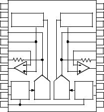
FUNCTIONAL DESCRIPTION
The AD1865 is a complete, monolithic, dual 18-bit audio DAC. No external components are required for operation. As shown in the block diagram, each chip contains two voltage references, two output amplifiers, two 18-bit serial input registers and two 18-bit DACs.
The voltage reference section provides a reference voltage for each DAC circuit. These voltages are produced by low-noise bandgap circuits. Buffer amplifiers are also included. This combination of elements produces reference voltages that are unaffected by changes in temperature and age.
The output amplifiers use both MOS and bipolar devices and incorporate an all NPN output stage. This design technique produces higher slew rate and lower distortion than previous techniques. Frequency response is also improved. When combined with the appropriate on-chip feedback resistor, the output op amps convert the output current to output voltages.
The 18-bit D/A converters use a combination of segmented decoder and R-2R architecture to achieve consistent linearity and differential linearity. The resistors which form the ladder structure are fabricated with silicon chromium thin film. Laser trimming of these resistors further reduces linearity errors resulting in low output distortion.
The input registers are fabricated with CMOS logic gates. These gates allow the achievement of fast switching speeds and low power consumption, contributing to the low glitch and low power dissipation of the AD1865.
–VS |
1 |
|
AD1865 |
|
24 |
+VS |
||
TRIM |
2 |
REFERENCE |
REFERENCE |
23 |
TRIM |
|||
MSB |
3 |
22 |
MSB |
|||||
|
|
|
|
|||||
IOUT |
4 |
|
|
|
|
21 |
IOUT |
|
AGND |
5 |
|
|
|
|
20 |
AGND |
|
SJ |
6 |
|
|
|
|
19 |
SJ |
|
RF |
7 |
|
|
|
|
18 |
RF |
|
VOUT |
8 |
|
|
|
|
17 |
VOUT |
|
+VL |
9 |
|
|
|
|
16 |
NC |
|
DR |
10 |
18-BIT |
18-BIT 18-BIT |
18-BIT |
15 |
DL |
||
LR |
11 |
LATCH |
D/A |
D/A |
LATCH |
14 |
LL |
|
|
|
|
|
|||||
CLK |
12 |
|
|
|
|
13 |
DGND |
|
NC = NO CONNECT
AD1865 Block Diagram (DIP Package)
–4– |
REV. 0 |
Loading...