


AD1891JP
Table of contents
 Loading...
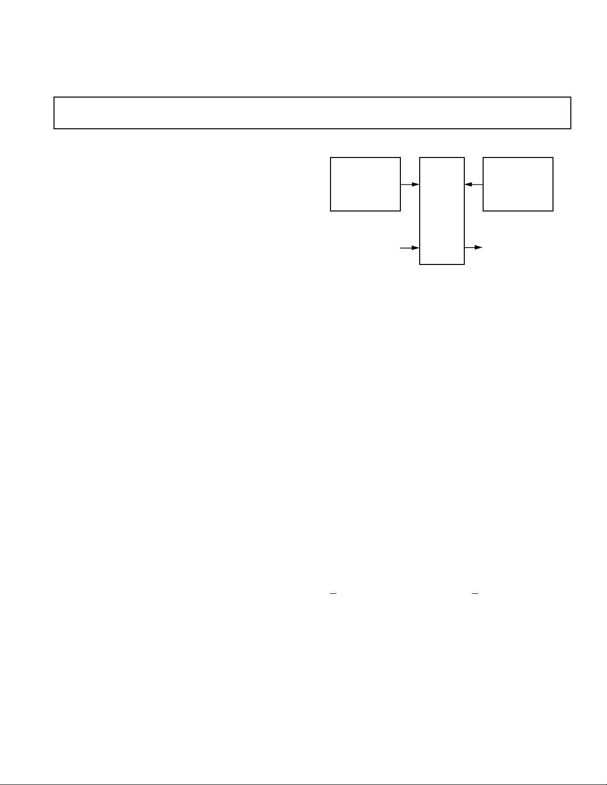
SYSTEM DIAGRAM
EXAMPLE
FREQUENCIES:
DAT 48kHz OR
CD 44.1kHz OR
BROADCAST 32kHz
AD1890/
AD1891
OUTPUT SAMPLE CLOCKINPUT SAMPLE CLOCK
INPUT SERIAL DATA
OUTPUT SERIAL DATA
EXAMPLE
FREQUENCIES:
DAT 48kHz OR
CD 44.1kHz OR
BROADCAST 32kHz
REV. 0
Information furnished by Analog Devices is believed to be accurate and
reliable. However, no responsibility is assumed by Analog Devices for its
use, nor for any infringements of patents or other rights of third parties
which may result from its use. No license is granted by implication or
otherwise under any patent or patent rights of Analog Devices.
a
SamplePort Stereo Asynchronous
Sample Rate Converters
AD1890/AD1891
One Technology Way, P.O. Box 9106, Norwood, MA 02062-9106, U.S.A.
Tel: 617/329-4700 Fax: 617/326-8703
FEATURES
Automatically Sense Sample Frequencies—No
Programming Required
Tolerant of Sample Clock Jitter
Smooth Transition When Sample Clock Frequencies
Cross
Accommodate Dynamically Changing Asynchronous
Sample Clocks
8 kHz to 56 kHz Sample Clock Frequency Range
1:2 to 2:1 Ratio Between Sample Clocks
–106 dB THD+N at 1 kHz (AD1890)
120 dB Dynamic Range (AD1890)
Optimal Clock Tracking Control
–Short/Long Group Delay Modes
–Slow/Fast Settling Modes
Linear Phase in All Modes
Equivalent of 4 Million 22-Bit FIR Filter Coefficients
Stored On-Chip
Automatic Output Mute
Flexible Four Wire Serial Interfaces
Low Power
APPLICATIONS
Digital Mixing Consoles and Digital Audio Workstations
CD-R, DAT, DCC and MD Recorders
Multitrack Digital Audio and Video Tape Recorders
Studio to Transmitter Links
Digital Audio Signal Routers/Switches
Digital Audio Broadcast Equipment
High Quality D/A Converters
Digital Tape Recorder Varispeed Applications
Computer Communication and Multimedia Systems
PRODUCT OVERVIEW
The AD1890 and AD1891 SamplePorts™ are fully digital, stereo
Asynchronous Sample Rate Converters (ASRCs) that solve sample
rate interfacing and compatibility problems in digital audio equip-
ment. Conceptually, these converters interpolate the input data up
to a very high internal sample rate with a time resolution of 300 ps,
then decimate down to the desired output sample rate. The
AD1890 is intended for 18- and 20-bit professional applications,
and the AD1891 is intended for 16-bit lower cost applications
where large dynamic sample-rate changes are not encountered.
These devices are asynchronous because the frequency and phase
relationships between the input and output sample clocks (both are
inputs to the AD1890/AD1891 ASRCs) are arbitrary and need not
be related by a simple integer ratio. There is no need to explicitly
select or program the input and output sample clock frequencies, as
the AD1890/AD1891 automatically sense the relationship between
SamplePort and SamplePorts are trademarks of Analog Devices, Inc.
the two clocks. The input and output sample clock frequencies
can nominally range from 8 kHz to 56 kHz, and the ratio
between them can vary from 1:2 to 2:1.
The AD1890/AD1891 use multirate digital signal processing
techniques to construct an output sample stream from the input
sample stream. The input word width is 4 to 20 bits for the
AD1890 or 4 to 16 bits for the AD1891. Shorter input words
are automatically zero-filled in the LSBs. The output word
width for both devices is 24 bits. The user can receive as many
of the output bits as desired. Internal arithmetic is performed
with 22-bit coefficients and 27-bit accumulation. The digital
samples are processed with unity gain.
The input and output control signals allow for considerable flex-
ibility for interfacing to a variety of DSP chips, AES/EBU
receivers and transmitters and for I
2
S compatible devices. Input
and output data can be independently justified to the left/right
clock edge, or delayed by one bit clock from the left/right clock
edge. Input and output data can also be independently justified
to the word clock rising edge or delayed by one bit clock from
the word clock rising edge. The bit clocks can also be indepen-
dently configured for rising edge active or falling edge active
operation.
The AD1890/AD1891 SamplePort™ ASRCs have on-chip digi-
tal coefficients that correspond to a highly oversampled 0 kHz to
20 kHz low-pass filter with a flat passband, a very narrow tran-
sition band, and a high degree of stopband attenuation. A subset
of these filter coefficients are dynamically chosen on the basis of
the filtered instantaneous ratio between the input sample clock
(L
R_I) and the output sample clock (LR_O), and these coeffi-
cients are used in an FIR convolver to perform the sample rate
conversion. Refer to the “Theory of Operation” section of this
data sheet for a more thorough functional description. The low-
pass filter has been designed so that full 20 kHz bandwidth is
maintained when the input and output sample clock frequencies
are as low as 44.1 kHz. If the output sample rate drops below
the input sample rate, the bandwidth of the input signal is
(continued on Page 4)
AD1890/AD1891–SPECIFICATIONS
TEST CONDITIONS UNLESS OTHERWISE NOTED
Supply Voltage +5.0 V
Ambient Temperature 25 °C
MCLK 20 MHz
Load Capacitance 100 pF
All minimums and maximums tested except as noted.
PERFORMANCE (Guaranteed over 0°C ≤ T
A
≤ 70°C, V
DD
= 5.0 V ± 10%, 8 MHz ≤ MCLK ≤ 20 MHz)
Min Max Units
AD1890 Dynamic Range (20 Hz to 20 kHz, –60 dB Input)† 120 dB
AD1891 Dynamic Range (20 Hz to 20 kHz, –60 dB Input)† 96 dB
Total Harmonic Distortion + Noise† dB
AD1890 and AD1891 (20 Hz to 20 kHz, Full-Scale Input,
F
SOUT
/F
SIN
Between 0.5 and 2.0) –94 dB
AD1890 (1 kHz Full-Scale Input, F
SOUT
/F
SIN
Between 0.7 and 1.4) –106 dB
AD1890 (10 kHz Full-Scale Input, F
SOUT
/F
SIN
Between 0.7 and 1.4) –100 dB
AD1891 (1 kHz Full-Scale Input, F
SOUT
/F
SIN
Between 0.7 and 1.4) –96 dB
AD1891 (10 kHz Full-Scale Input, F
SOUT
/F
SIN
Between 0.7 and 1.4) –95 dB
Interchannel Phase Deviation† 0 Degrees
Input and Output Sample Clock Jitter† 10 ns
(For
≤
1 dB Degradation in THD+N with 10 kHz Full-Scale Input, Slow-Settling Mode)
DIGITAL INPUTS (Guaranteed over 0°C ≤ T
A
≤ 70°C, V
DD
= 5.0 V ± 10%, 8 MHz ≤ MCLK ≤ 20 MHz)
Min Max Units
V
IH
2.2 V
V
IL
0. 8 V
I
IH
@ V
IH
= +5 V 4 µA
I
IL
@ V
IL
= 0 V 4 µA
V
OH
@ I
OH
= –4 mA 3.6 V
V
OL
@ I
OL
= 4 mA 0.4 V
Input Capacitance† 15 pF
DIGITAL TIMING (Guaranteed over 0°C ≤ T
A
≤ 70°C, V
DD
= 5.0 V ± 10%, 8 MHz ≤ MCLK ≤ 20 MHz)
Min Max Units
t
MCLK
MCLK Period 50 125 ns
f
MCLK
MCLK Frequency (1/t
MCLK
) 8 20 MHz
t
MPWL
MCLK LO Pulse Width 20 ns
t
MPWH
MCLK HI Pulse Width 20 ns
f
LRI
LR_I Frequency with 20 MHz MCLK† 10 70 kHz
t
RPWL
RESET LO Pulse Width 100 ns
t
RS
RESET Setup to MCLK Falling 15 ns
t
BCLK
BCLK_I/O Period† 80 ns
f
BCLK
BCLK_I/O Frequency (l/t
BCLK
)† 12.5 MHz
t
BPWL
BCLK_I/O LO Pulse Width 40 ns
t
BPWH
BCLK_I/O HI Pulse Width 40 ns
t
WSI
WCLK_I Setup to BCLK_I 15 ns
t
WSO
WCLK_O Setup to BCLK_O 30 ns
t
LRSI
LR_I Setup to BCLK_I 15 ns
t
LRSO
LR_O Setup to BCLK_O 30 ns
t
DS
Data Setup to BCLK_I 0 ns
t
DH
Data Hold from BCLK_I 25 ns
t
DPD
Data Propagation Delay from BCLK_O 40 ns
t
DOH
Data Output Hold from BCLK_O 5 ns
REV. 0
–2–

AD1890/AD1891
REV. 0
–3–
POWER (0°C ≤ T
A
≤ 70°C, MCLK = 16 MHz, F
SIN
= 48 kHz, F
SOUT
= 44.1 kHz)
Min Typ Max Units
Supplies
Voltage, V
DD
2.7 5.5 V
Current, I
DD
(V
DD
= 5.0 V) 35 40 mA
Current, I
DD
(V
DD
= 3.0 V) 19 mA
Dissipation
Operation (V
DD
= 5.0 V) 175 200 mW
Operation (V
DD
= 3.0 V) 57 mW
TEMPERATURE RANGE
Min Max Units
Specifications Guaranteed 0 +70 °C
Operation Guaranteed –40 +85 °C
Storage –60 +100 °C
ABSOLUTE MAXIMUM RATINGS*
Min Max Units
V
DD
to GND –0.3 7.0 V
DC Input Voltage –0.3 V
DD
+ 0.3 V
Latch-Up Trigger Current –1000 +1000 mA
Soldering +300 °C
10 sec
*Stresses greater than those listed under “Absolute Maximum Ratings” may cause permanent damage to the device. This is a stress rating only and functional operation
of the device at these or any other conditions above those indicated in the operational section of this specification is not implied. Exposure to absolute maximum rating
conditions for extended periods may affect device reliability.
DIGITAL FILTER CHARACTERISTICS†
Min Max Units
Passband Ripple (0 to 20 kHz) 0.01 dB
Transition Band
1
4. 1 kHz
Stopband Attenuation 110 dB
Group Delay (LR
–
I = 50 kHz) 700 3000 µs
†Guaranteed. Not Tested
1
Valid only when F
SOUT
≥ F
SIN
(i.e., upsampling), F
SIN
= 44.1 kHz.
Specifications subject to change without notice.
ORDERING GUIDE
Model Temperature Range Package Description Package Option
AD1890JN 0°C to +70°C Plastic DIP N-28
AD1890JP 0°C to +70°C PLCC P-28A
AD1891JN 0°C to +70°C Plastic DIP N-28
AD1891JP 0°C to +70°C PLCC P-28A
WARNING!
ESD SENSITIVE DEVICE
CAUTION
ESD (electrostatic discharge) sensitive device. Electrostatic charges as high as 4000 V readily
accumulate on the human body and test equipment and can discharge without detection.
Although the AD1890/AD1891 features proprietary ESD protection circuitry, permanent
damage may occur on devices subjected to high energy electrostatic discharges. Therefore,
proper ESD precautions are recommended to avoid performance degradation or loss of
functionality.
AD1890/AD1891
–4–
REV. 0
(continued from Page 1)
PRODUCT OVERVIEW (Continued)
automatically limited to avoid alias distortion on the output sig-
nal. The AD1890/AD1891 dynamically alter the low-pass filter
cutoff frequency smoothly and slowly, so that real-time varia-
tions in the sample rate ratio are possible without degradation of
the audio quality.
The AD1890/AD1891 have a pin selectable slow- or fast-settling
mode. This mode determines how quickly the ASRCs adapt to a
change in either the input sample clock frequency (F
SIN
) or the
output sample clock frequency (F
SOUT
). In the slow-settling
mode, the control loop which computes the ratio between F
SIN
and F
SOUT
settles in approximately 800 ms and begins to reject
jitter above 3 Hz. The slow-settling mode offers the best signal
quality and the greatest jitter rejection. In the fast-settling mode,
the control loop settles in approximately 200 ms and begins to
reject jitter above 12 Hz. The fast-settling mode allows rapid,
real time sample rate changes to be tracked without error, at the
expense of some narrow-band noise modulation products on the
output signal.
The AD1890 also has a pin selectable, short or long group delay
mode. This pin determines the depth of the First-In, First-Out
(FIFO) memory which buffers the input data samples before
they are processed by the FIR convolver. In the short mode, the
group delay is approximately 700 µs. The ASRC is more sensi-
tive to sample rate changes in this mode (i.e., the pointers which
manage the FIFO are more likely to cross and become momen-
tarily invalid during a sample rate step change), but the group
delay is minimized. In the long mode, the group delay is ap-
proximately 3 ms. The ASRC is tolerant of large dynamic
sample rate changes in this mode, and it should be used when
the device is required to track fast sample rate changes, such as
in varispeed applications. The AD1891 features the short group
delay mode only. In either device, if the read and write pointers
that manage the FIFO cross (indicating underflow or overflow),
the ASRC asserts the mute output (MUTE_O) pin HI for 128
output clock cycles. If MUTE_O is connected to the mute input
(MUTE_I) pin, as it normally should be, the serial output will
be muted (i.e., all bits zero) during this transient event.
The AD1890/AD1891 are fabricated in a 0.8µm single poly,
double metal CMOS process and are packaged in a 0.6" wide
28-pin plastic DIP and a 28-pin PLCC. The AD1890/AD1891
operate from a +5 V power supply over the temperature range of
0°C to +70°C.
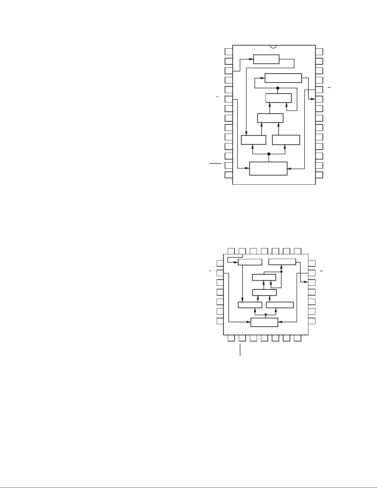
28
27
26
22
21
20
19
18
17
25
24
23
16
15
SERIAL IN
SERIAL OUT
MULT
CLOCK
TRACKING
ACCUM
RESET
LR_I
LR_O
1
2
3
7
8
9
10
11
12
4
5
6
13
14
COEF ROM
FIFO
GPDLYS (AD1890)
N/C (AD1891)
MCLK
DATA_I
BCLK_I
WCLK_I
V
DD
GND
N/C
BKPOL_I
TRGLR_I
MSBDLY_I
GND
SETSLW
GND
BCLK_O
WCLK_O
DATA_O
V
DD
GND
N/C
BKPOL_O
TRGLR_O
MSBDLY_O
MUTE_O
MUTE_I
AD1890/AD1891
N/C = NO CONNECT
AD1890/AD1891 DIP Pinout
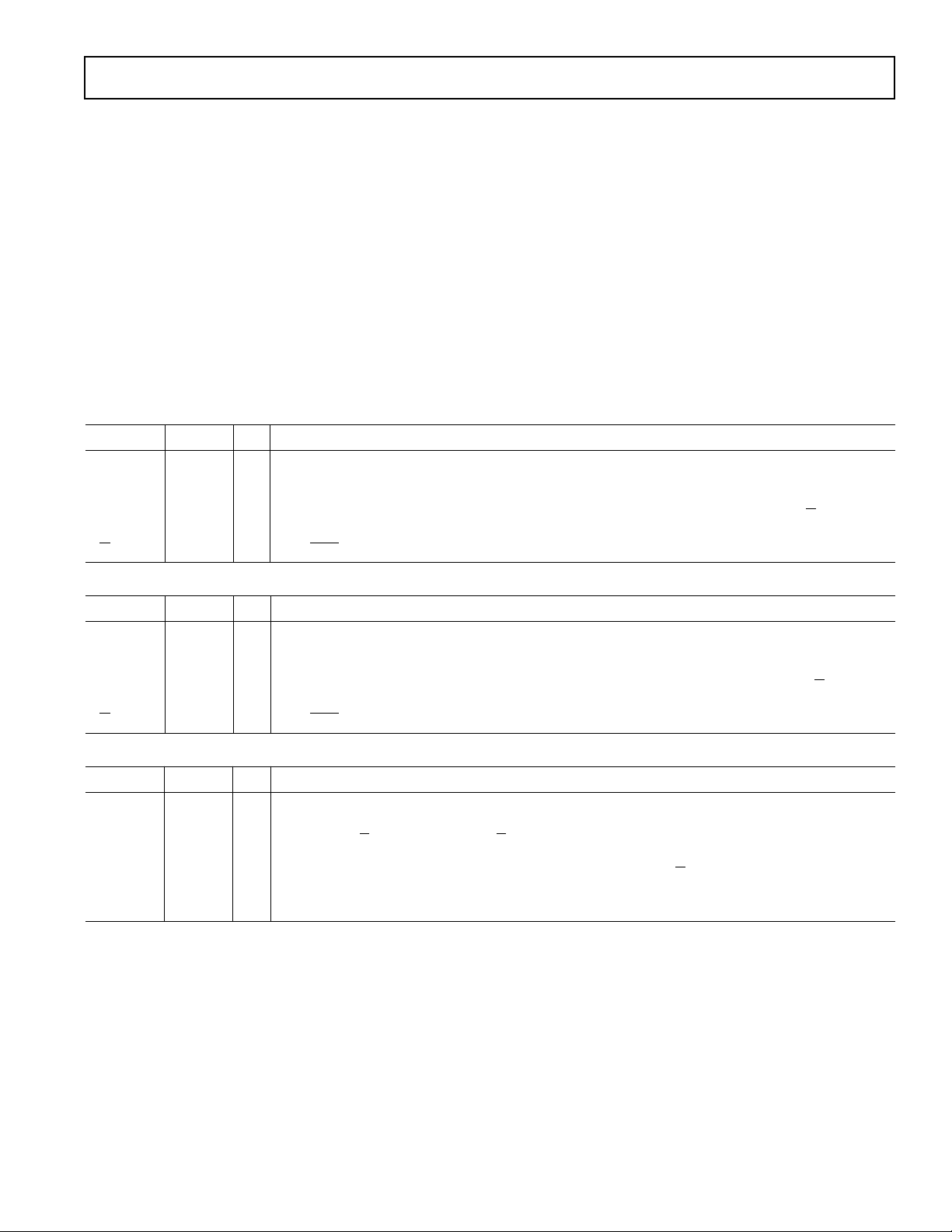
22
21
20
19
25
24
23
7
8
9
10
11
5
6
LR_I
LR_O
SERIAL IN
RESET
SERIAL OUT
ACCUM
COEF ROM
FIFO
MULT
N/C
WCLK_I
V
DD
GND
BKPOL_I
TRGLR_I
WCLK_O
DATA_O
V
DD
GND
N/C
BKPOL_O
1234 282726
12 13 14 18171615
GPDLYS (AD1890)
N/C (AD1891)
MCLK
DATA_I
BCLK_I
SETLSLW
GND
BCLK_O
MSBDLY_I
GND
TRGLR_O
MSBDLY_O
MUTE_O
MUTE_I
CLOCK
TRACKING
AD1890/AD1891
N/C = NO CONNECT
AD1890/AD1891 PLCC Pinout
AD1890/AD1891
REV. 0
–5–
AD1890/AD1891 PIN LIST
Serial Input Interface
Pin Name Number I/O Description
DATA_I 3 I Serial input, MSB first, containing two channels of 4- to 20-bits of twos-complement data per
channel. AD1891 ONLY: Maximum of 16 data bits per channel; additional bits ignored.
BCLK_I 4 I Bit clock input for input data.
WCLK_I 5 I Word clock input for input data. This input is rising edge sensitive. (Not required in L
R input data
clock triggered mode [TRGLR_I = HI].)
LR_I 6 I Left/right clock input for input data. Must run continuously.
Serial Output Interface
Pin Name Number I/O Description
DATA_O 23 O Serial output, MSB first, containing two channels of 4- to 24-bits of twos-complement data per
channel.
BCLK_O 26 I Bit clock input for output data.
WCLK_O 25 I Word clock input for output data. This input is rising edge sensitive. (Not required in L
R output
data clock triggered mode [TRGLR_O = HI].)
LR_O 24 I Left/right clock input for output data. Must run continuously.
Input Control Signals
Pin Name Number I/O Description
BKPOL_I 10 I Bit clock polarity. LO: Normal mode. Input data is sampled on rising edges of BCLK_I. HI:
Inverted mode. Input data is sampled on falling edges of BCLK_I.
TRGLR_I 11 I Trigger on L
R_I. HI: Changes in LR_I indicate beginning
1
of valid input data. LO: Rising edge of
WCLK_I indicates beginning of valid input data.
MSBDLY_I 12 I MSB delay. HI: Input data is delayed one BCLK_I after either L
R_I (TRGLR_I = HI) or WCLK_I
(TRGLR_I = LO) indicates the beginning of valid input data. Included for I
2
S data format
compatibility. LO: No delay.
NOTE
1
The beginning of valid data will be delayed by one BLCK_I if MSBDEL_I is selected (HI).
Group Delay
Intuitively, the time interval required for a full-level input pulse
to appear at the converter’s output, at full level, expressed in
milliseconds (ms). More precisely, the derivative of radian phase
with respect to radian frequency at a given frequency.
Transport Delay
The time interval between when an impulse is applied to the
converters input and when the output starts to be affected by
this impulse, expressed in milliseconds (ms). Transport delay is
independent of frequency.
DEFINITIONS
Dynamic Range
The ratio of a near full-scale input signal to the integrated noise
in the passband (0 to ≈20 kHz), expressed in decibels (dB). Dy-
namic range is measured with a –60 dB input signal and
“60 dB” arithmetically added to the result.
Total Harmonic Distortion + Noise
Total Harmonic Distortion plus Noise (THD+N) is defined as
the ratio of the square root of the sum of the squares of the val-
ues of the harmonics and noise to the rms value of a sinusoidal
input signal. It is usually expressed in percent (%) or decibels.
Interchannel Phase Deviation
Difference in input sampling times between stereo channels, ex-
pressed as a phase difference in degrees between 1 kHz inputs.
AD1890/AD1891
–6–
REV. 0
Output Control Signals
Pin Name Number I/O Description
BKPOL_O 19 I Bit clock polarity. LO: Normal mode. Output data is valid on rising edges of BCLK_O, changed
on falling. HI: Inverted mode. Output data is valid on falling edges of BCLK_O, changed on rising.
TRGLR_O 18 I Trigger on L
R_O. HI: Changes in LR_O indicate beginning
1
of valid output data. LO: Rising
edge of WCLK_O indicates beginning of valid output data.
MSBDLY_O 17 I MSB delay. HI: Output data is delayed one BCLK_O after either L
R_O (TRGLR_O = HI) or
WCLK_O (TRGLR_O = LO) indicates the beginning of valid output data. Included for I
2
S data
format compatibility. LO: No delay.
Miscellaneous
Pin Name Number I/O Description
GPDLYS 1 I AD1890 ONLY: Group delay—short. HI: Short group delay mode (≈700 µs). More sensitive to
changes in sample rates (L
R clocks). LO: Long group delay mode (≈3 ms). More tolerant of
sample rate changes. This signal may be asynchronous with respect to MCLK, and dynamically
changed, but is normally pulled up or pulled down on a static basis. AD1891: Short group delay
mode only; this pin is a N/C.
MCLK 2 I Master clock input. Nominally 16 MHz for sampling frequencies (F
S
, word rates) from 8 kHz to
56 kHz. Exact frequency is not critical, and does not need to be synchronized to any other clock
or possess low jitter.
RESET 13 I Active LO reset. Set HI for normal chip operation.
MUTE_O 16 O Mute output. HI indicates that data is not currently valid due to read and write FIFO memory
pointer overlap. LO indicates normal operation.
MUTE_I 15 I Mute input. HI mutes the serial output to zeros (midscale). Normally connected to MUTE_O.
Reset LO for normal operation.
SETLSLW 28 I Settle slowly to changes in sample rates. HI: Slow-settling mode (≈800 ms). Less sensitive to
sample clock jitter. LO: Fast-settling mode (≈200 ms). Some narrow-band noise modulation may
result from jitter on L
R clocks. This signal may be asynchronous with respect to MCLK, and
dynamically changed, but is normally pulled up or pulled down on a static basis.
N/C 9, 20 No connect. Reserved. Do not connect.
Power Supply Connections
Pin Name Number I/O Description
V
DD
7, 22 I Positive digital voltage supply.
GND 8, 14, 21, 27 I Digital ground. Pins 14 and 27 need not be decoupled.
NOTE
1
The beginning of valid data will be delayed by one BCLK_O if MSBDEL _O is selected (Hl).
Loading...