


AD5116
Table of contents
 Loading...
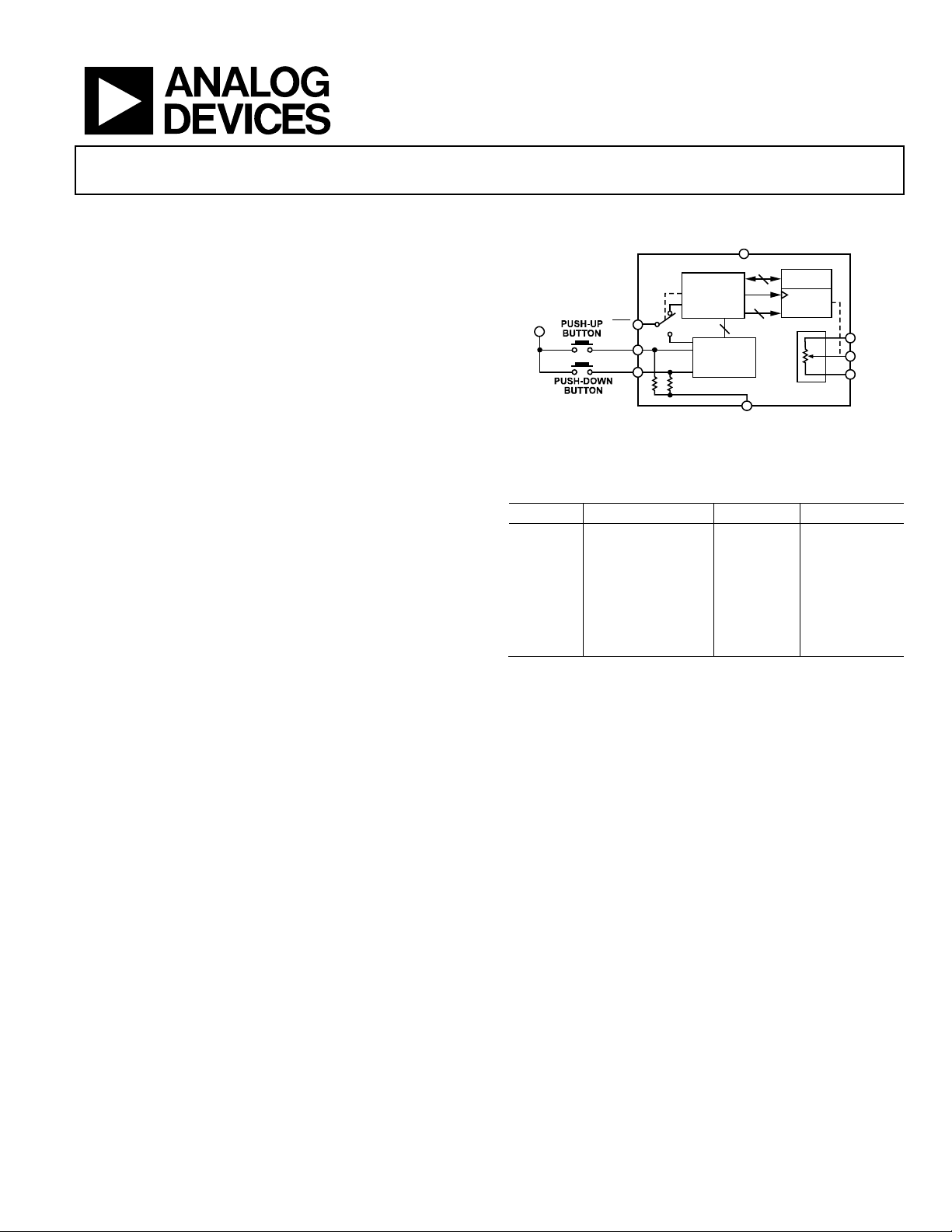
Single-Channel, 64-Position, Push Button,
±8% Resistor Tolerance, Nonvolatile Digital Potentiometer
Data Sheet
AD5116
Rev. A
Information furnished by Analog Devices is believed to be accurate and reliable. However, no
responsibility is assumed by Analog Devices for its use, nor for any infringements of patents or other
rights of third parties that may result from its use. Specifications subject to change without notice. No
license is granted by implication or otherwise under any patent or patent rights of Analog Devices.
Trademarks and registered trademarks are the property of their respective owners.
One Technology Way, P.O. Box 9106, Norwood, MA 02062-9106, U.S.A.
Tel: 781.329.4700 www.analog.com
Fax: 781.461.3113 ©2011–2012 Analog Devices, Inc. All rights reserved.
FEATURES
Nominal resistor tolerance error: ±8% maximum
Wiper current: ±6 mA
Rheostat mode temperature coefficient: 35 ppm/°C
Low power consumption: 2.5mA max @ 2.7 V and 125°C
Wide bandwidth: 4 MHz (5 kΩ option)
Power-on EEPROM refresh time < 50 μs
50-year typical data retention at 125°C
1 million write cycles
2.3 V to 5.5 V supply operation
Built-in adaptive debouncer
Wide operating temperature: −40°C to +125°C
Thin, 2 mm × 2 mm × 0.55 mm 8-lead LFCSP package
APPLICATIONS
Mechanical potentiometer replacement
Portable electronics level adjustment
Audio volume control
Low resolution DAC
LCD panel brightness and contrast control
Programmable voltage to current conversion
Programmable filters, delays, time constants
Feedback resistor programmable power supply
Sensor calibration
FUNCTIONAL BLOCK DIAGRAM
ADAPTIVE
DEBOUNCER
CONTROL
LOGIC
BLOCK
EEPROM
RDAC
REGISTER
AD5116
A
W
B
DATA
DATA
GND
V
DD
V
DD
09657-001
ASE
PU
PD
Figure 1.
Table 1. NVM ±8% Resistance Tolerance Family
Model Resistance (kΩ) Position Interface
AD5110 10, 80 128 I
2
C
AD5111 10, 80 128 Up/down
AD5112 5, 10, 80 64 I
2
C
AD5113 5, 10, 80 64 Up/down
AD5116 5, 10, 80 64 Push button
AD5114 10, 80 32 I
2
C
AD5115 10, 80 32 Up/down
GENERAL DESCRIPTION
The AD5116 provides a nonvolatile digital potentiometer
solution for 64-position adjustment applications, offering
guaranteed low resistor tolerance errors of ±8% and up to
±6 mA current density in the A, B, and W pins. The low resistor
tolerance, low nominal temperature coefficient, and high
bandwidth simplify open-loop applications, as well as tolerance
matching applications.
The new low A-W and B-W resistance feature minimizes
the wiper resistance in the extremes of the resistor array to
typically 45 Ω.
A simple push button interface allows manual control with
just two external push button switches. The AD5116 is designed
with a built-in adaptive debouncer that ignores invalid bounces
due to contact bounce (commonly found in mechanical
switches). The debouncer is adaptive, accommodating a
variety of push buttons.
The AD5116 can automatically save the last wiper position into
EEPROM, making it suitable for applications that require a
power-up in the last wiper position, for example, audio
equipment.
The AD5116 is available in a 2 mm × 2 mm 8-lead LFCSP
package. The part is guaranteed to operate over the extended
industrial temperature range of −40°C to +125°C.

AD5116 Data Sheet
Rev. A | Page 2 of 16
TABLE OF CONTENTS
Features .............................................................................................. 1
Applications ....................................................................................... 1
Functional Block Diagram .............................................................. 1
General Description ......................................................................... 1
Revision History ............................................................................... 2
Specifications ..................................................................................... 3
Electrical Characteristics ............................................................. 3
Interface Timing Specifications .................................................. 5
Timing Diagrams .......................................................................... 5
Absolute Maximum Ratings ............................................................ 6
Thermal Resistance ...................................................................... 6
ESD Caution .................................................................................. 6
Pin Configuration and Function Descriptions ............................. 7
Typical Performance Characteristics ............................................. 8
Test Circuits ..................................................................................... 12
Theory of Operation ...................................................................... 13
RDAC Register ............................................................................ 13
EEPROM ..................................................................................... 13
Automatic Save Enable .............................................................. 13
End Scale Resistance Indicator ................................................. 14
RDAC Architecture .................................................................... 14
Programming the Variable Resistor ......................................... 14
Programming the Potentiometer Divider ............................... 15
Terminal Voltage Operating Range ......................................... 15
Power-Up Sequence ................................................................... 15
Layout and Power Supply Biasing ............................................ 15
Outline Dimensions ....................................................................... 16
Ordering Guide .......................................................................... 16
REVISION HISTORY
4/12—Rev. 0 to Rev. A
Changes to Features Section............................................................ 1
Changes to Positive Supply Current, Table 2 ................................ 4
Changes to Ordering Guide .......................................................... 16
10/11—Revision 0: Initial Version

Data Sheet AD5116
Rev. | Page 3 of 16
SPECIFICATIONS
ELECTRICAL CHARACTERISTICS
5 kΩ, 10 kΩ, and 80 kΩ versions: V
DD
= 2.3 V to 5.5 V, V
A
= V
DD
, V
B
= 0 V, −40°C < T
A
< +125°C, unless otherwise noted.
Table 2.
Parameter Symbol Test Conditions/Comments Min Typ
1
Max Unit
DC CHARACTERISTICS—RHEOSTAT MODE
Resolution N 6 Bits
Resistor Integral Nonlinearity
2
R-INL R
AB
= 5 kΩ, V
DD
= 2.3 V to 2.7 V −2.5 ±0.5 +2.5 LSB
R
AB
= 5 kΩ, V
DD
= 2.7 V to 5.5 V −1 ±0.25 +1 LSB
R
AB
= 10 kΩ −1 ±0.25 +1 LSB
R
AB
= 80 kΩ −0.25 ±0.1 +0.25 LSB
Resistor Differential Nonlinearity
2
R-DNL −1 ±0.25 +1 LSB
Nominal Resistor Tolerance ΔR
AB
/R
AB
−8 +8 %
Resistance Temperature Coefficient
3
(ΔR
AB
/R
AB
)/ΔT × 10
6
Code = full scale 35 ppm/°C
Wiper Resistance
R
W
Code = zero scale
70
140
Ω
R
BS
Code = bottom scale 45 80 Ω
R
TS
Code = top scale 70 140 Ω
DC CHARACTERISTICS—POTENTIOMETER
DIVIDER MODE
Integral Nonlinearity
4
INL −0.5 ±0.15 +0.5 LSB
Differential Nonlinearity
4
DNL −0.5 ±0.15 +0.5 LSB
Full-Scale Error V
WFSE
R
AB
= 5 kΩ −2.5 LSB
R
AB
=10 kΩ
−1.5
LSB
R
AB
= 80 kΩ −1 LSB
Zero-Scale Error V
WZSE
R
AB
= 5 kΩ +1.5 LSB
R
AB
=10 kΩ +1 LSB
R
AB
= 80 kΩ +0.25 LSB
Voltage Divider Temperature Coefficient
3
(ΔV
W
/V
W
)/ΔT × 10
6
Code = half scale ±10 ppm/°C
RESISTOR TERMINALS
Maximum Continuous I
A
, I
B
, and I
W
Current
3
R
AB
= 5 kΩ, 10 kΩ −6 +6 mA
R
AB
= 80 kΩ
−1.5
+1.5
mA
Terminal Voltage Range
5
GND V
DD
V
Capacitance A, Capacitance B
3, 6
C
A
, C
B
f = 1 MHz, measured to GND,
code = half scale, V
W
= V
A
= 2.5 V
or V
W
= V
B
= 2.5 V
20 pF
Capacitance W
3, 6
C
W
f = 1 MHz, measured to GND,
code = half scale, V
A
= V
B
= 2.5 V
35 pF
Common-Mode Leakage Current
3
V
A
= V
W
= V
B
50 nA
DIGITAL INPUTS (PU AND PD)
Input Logic
3
High V
INH
2 V
Low V
INL
0.8 V
Input Current
3
I
N
±1 µA
Input Capacitance
3
C
IN
5 pF
DIGITAL OUTPUT (ASE)
Output High Voltage
3
V
OH
I
SINK
= 2 mA, V
DD
= 5 V
4.8
V
Output Current
3
I
O
V
DD
= 5 V 16 mA
Three-State Leakage Current
3
I
OZ
±1 µA
Input Capacitance
3
C
IN
5 pF
A

AD5116 Data Sheet
Rev. A | Page 4 of 16
Parameter Symbol Test Conditions/Comments Min Typ
1
Max Unit
POWER SUPPLIES
Single-Supply Power Range 2.3 5.5 V
Positive Supply Current I
DD
V
DD
= 5 V 0.75 3.5 mA
V
DD
= 2.7 V 2.5 mA
V
DD
= 2.3 V 2.4 mA
EEMEM Store Current
3, 7
I
DD_NVM_STORE
2 mA
EEMEM Read Current
3, 8
I
DD_NVM_READ
320 μA
Power Dissipation
9
P
DISS
V
IH
= V
LOGIC
or V
IL
= GND 5 μW
Power Supply Rejection
3
PSR ∆V
DD
/∆V
SS
= 5 V ± 10%
R
AB
= 5 kΩ −43 dB
R
AB
=10 kΩ −50 dB
R
AB
= 80 kΩ −64 dB
DYNAMIC CHARACTERISTICS
3, 10
Bandwidth BW Code = half scale − 3 dB
R
AB
= 5 kΩ 4 MHz
R
AB
= 10 kΩ 2 MHz
R
AB
= 80 kΩ 200 kHz
Total Harmonic Distortion THD V
A
= V
DD
/2 + 1 V rms, V
B
= V
DD
/2,
f = 1 kHz, code = half scale
R
AB
= 5 kΩ −75 dB
R
AB
= 10 kΩ −80 dB
R
AB
= 80 kΩ −85 dB
V
W
Settling Time t
s
V
A
= 5 V, V
B
= 0 V, ±0.5 LSB error
band
R
AB
= 5 kΩ 2.5 μs
R
AB
= 10 kΩ 3 μs
R
AB
= 80 kΩ 10 μs
Resistor Noise Density e
N_WB
Code = half scale, T
A
= 25°C,
f = 100 kHz
R
AB
= 5 kΩ 7 nV/√Hz
R
AB
= 10 kΩ 9 nV/√Hz
R
AB
= 80 kΩ 20 nV/√Hz
FLASH/EE MEMORY RELIABILITY
3
Endurance
11
T
A
= 25°C 1 MCycles
100 kCycles
Data Retention
12
50 Years
1
Typical values represent average readings at 25°C, VDD = 5 V, V
SS
= 0 V, and V
LOGIC
= 5 V.
2
Resistor position nonlinearity error (R-INL) is the deviation from an ideal value measured between the maximum resistance and the minimum resistance wiper
positions. R-DNL measures the relative step change from ideal between successive tap positions. The maximum wiper current is limited to 0.8 × V
DD
/R
AB
.
3
Guaranteed by design and characterization, not subject to production test.
4
INL and DNL are measured at V
WB
with the RDAC configured as a potentiometer divider similar to a voltage output DAC. V
A
= V
DD
and V
B
= 0 V. DNL specification limits
of ±1 LSB maximum are guaranteed monotonic operating conditions.
5
Resistor Terminal A, Resistor Terminal B, and Resistor Terminal W have no limitations on polarity with respect to each other.
6
C
A
is measured with V
W
= V
A
= 2.5 V, C
B
is measured with V
W
= V
B
= 2.5 V, and C
W
is measured with V
A
= V
B
= 2.5 V.
7
Different from operating current; supply current for NVM program lasts approximately 30 ms.
8
Different from operating current; supply current for NVM read lasts approximately 20 μs.
9
P
DISS
is calculated from (I
DD
× V
DD
).
10
All dynamic characteristics use V
DD
= 5.5 V, and V
LOGIC
= 5 V.
11
Endurance is qualified at 100,000 cycles per JEDEC Standard 22, Method A117 and measured at 150°C.
12
Retention lifetime equivalent at junction temperature (T
J
) = 125°C per JEDEC Standard 22, Method A117. Retention lifetime based on an activation energy of 1 eV
derates with junction temperature in the Flash/EE memory.
Data Sheet AD5116
Rev. | Page 5 of 16
INTERFACE TIMING SPECIFICATIONS
V
DD
= 2.3 V to 5.5 V; all specifications T
MIN
to T
MAX
, unless otherwise noted.
Table 3.
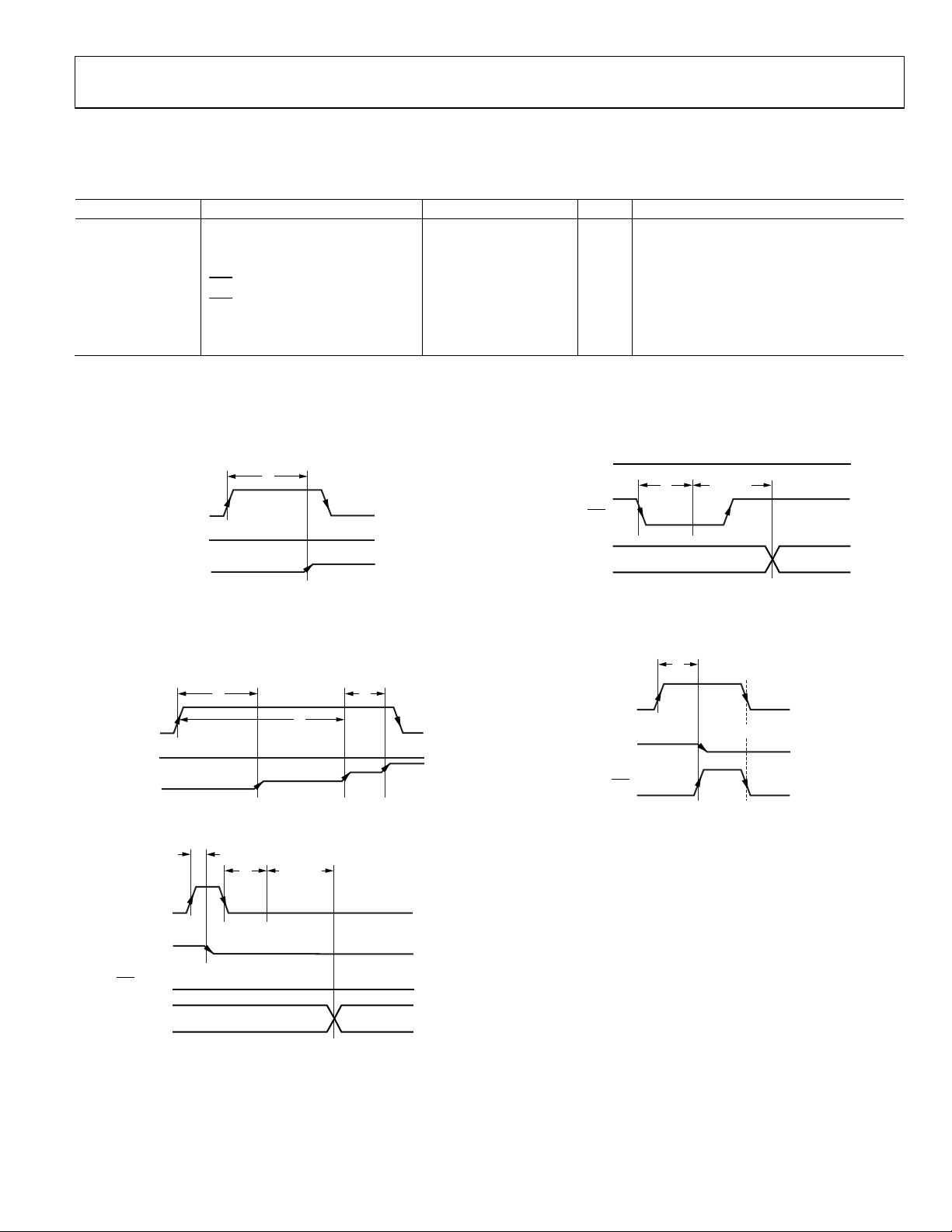
Parameter Test Conditions/Comments Min Typ Max Unit Description
t
1
8 ms Debounce time
t
2
1 sec Manual to auto scan time
t
3
140 ms Auto scan step
t
4
ASE
= 0 V, PD = GND, PU = GND
1 sec Auto save execute time
t
5
ASE
= V
DD
8 ms Low pulse time to manual storage
t
EEPROM_PROGRAM
1
15 50 ms Memory program time
t
POWER_UP
2
50 μs Power-on EEPROM restore time
1
EEPROM program time depends on the temperature and EEPROM write cycles. Higher timing is expected at a lower temperature and higher write cycles.
2
Maximum time after V
DD
is equal to 2.3 V.
TIMING DIAGRAMS
09657-002
PU
R
W
t
1
PD (LOW)
Figure 2. Manual Increment Mode Timing
09657-003
PU
t
1
t
2
t
3
PD (LOW)
R
W
Figure 3. Auto Increment Mode Timing
9657-004
PD
t
1
t
4
EEPROM DATA NEW DATA
t
EEPROM
PROGRAM
R
W
ASE (LOW)
Figure 4. Auto Save Mode Timing
09657-005
PD/PU (LOW)
t
5
EEPROM
DATA NEW DATA
t
EEPROM
PROGRAM
ASE
Figure 5. Manual Save Mode Timing
09657-006
PD
t
1
R
W
R
W
= 45Ω
ASE
Figure 6. End Scale Indication Timing
A
Loading...