


AD261BND-4
Table of contents
 Loading...
Analog Devices AD261BND-4, AD261BND-3, AD261BND-2, AD261BND-1, AD261BND-0 Datasheet
...
REV. 0
Information furnished by Analog Devices is believed to be accurate and
reliable. However, no responsibility is assumed by Analog Devices for its
use, nor for any infringements of patents or other rights of third parties
which may result from its use. No license is granted by implication or
otherwise under any patent or patent rights of Analog Devices.
a
AD261
One Technology Way, P.O. Box 9106, Norwood, MA 02062-9106, U.S.A.
Tel: 781/329-4700 World Wide Web Site: http://www.analog.com
Fax: 781/326-8703 © Analog Devices, Inc., 1997
High Speed, Logic Isolator
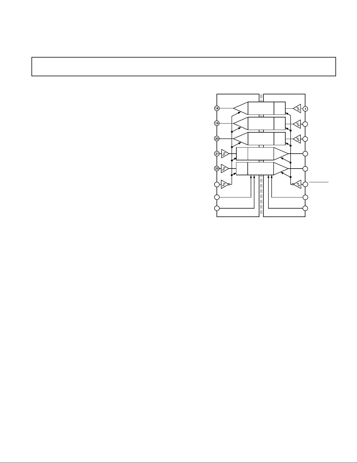
FUNCTIONAL BLOCK DIAGRAM
TYPICAL MODEL
(AD261-2)
S0
F3
SYSTEM
FIELD
+5V dc
5Vdc RTN
+5V dc
5Vdc RTN
S1
2
S2
3
S3
S4
F0
F1
F2
F4
15
16
17
6
7
8
5
THREE-
STATE
LATCH
E
D
LINE 0
+5V dc
FLD
5V RTN
FLD
ENABLE
FLD
5V RTN
SYS
+5V dc
SYS
ENABLE
SYS
THREE-
STATE
LATCH
E
D
LINE 1
THREE-
STATE
LATCH
E
D
LINE 2
LATCH
E
D
THREE-
STATE
LINE 4
LINE 3
LATCH
E
D
THREE-
STATE
4
FEATURES
Isolation Test Voltage: To 3.5 kV rms
Five Isolated Logic Lines: Available in Six I/O Configurations
Logic Signal Bandwidth: 20 MHz (min)
CMV Transient Immunity: 10 kV/ms min
Waveform Edge Transmission Symmetry: 61 ns
Field and System Output Enable/Three-State Functions
Performance Rated Over –258C to +858C
UL1950, IEC950, EN60950 Certification (VDE, CE, Pending)
APPLICATIONS
PLC/DCS Analog Input and Output Cards
Communications Bus Isolation
General Data Acquisition Applications
IGBT Motor Drive Controls
High Speed Digital I/O Ports
GENERAL DESCRIPTION
The AD261 is designed to isolate five digital control signals
to/from a microcontroller and its related field I/O components.
Six models allow all I/O combinations from five input lines to
five output lines, including combinations in between. Every
AD261 effectively replaces up to five opto-isolators.
Each line of the AD261 has a bandwidth of 20MHz (min) with
a propagation delay of only 14 ns, which allows for extremely
fast data transmission. Output waveform symmetry is maintained
to within ±1 ns of the input so the AD261 can be used to accu-
rately isolate time-based PWM signals.
All field or system output pins of the AD261 can be set to a high
resistance three-state level by use of the two enable pins. A field
output three-stated offers a convenient method of presetting
logic levels at power-up by use of pull-up/down resistors. Sys-
tem side outputs being three-stated allows for easy multiplexing
of multiple AD261s.
The isolation barrier of the AD261 B Grade is 100% tested
as high as 3.5 kV rms (system to field). The barrier design also
provides excellent common-mode transient immunity from
10 kV/µs common-mode voltage excursions of field side termi-
nals relative to the system side, with no false output triggering
on either side.
Each output is updated within nanoseconds by input logic tran-
sitions, the AD261 also has a continuous output update feature
that automatically updates each output based on the dc level of
the input. This guarantees the output is always valid 10µs after
a fault condition or after the power-up reset interval.
PRODUCT HIGHLIGHTS
Six Isolated Logic Line I/O Configurations Available: The
AD261 is available in six pin-compatible versions of I/O con-
figurations to meet a wide variety of requirements.
Wide Bandwidth with Minimal Edge Error: The AD261
affords extremely fast isolation of logic signals due to its 20MHz
bandwidth and 14 ns propagation delay. It maintains a wave-
form input-to-output edge transition error of typically less than
±1 ns (total) for positive vs. negative transition.
3.5 kV rms Test Voltage Isolation Rating: The AD261
B Grade is rated to operate at 1.25 kV rms and is 100% pro-
duction tested at 3.5 kV rms, using a standard ADI test method.
High Transient Immunity: The AD261 rejects common-
mode transients slewing at up to 10 kV/µs without false trigger-
ing or damage to the device.
(Continued on page 5)

–2–
REV. 0
AD261–SPECIFICA TIONS
(Typical at T
A
= +258C, +5 V dc
SYS
, +5 V dc
FLD
, t
RR
= 50 ns max unless otherwise noted)
Parameter Conditions Min Typ Max Units
INPUT CHARACTERISTICS
Threshold Voltage
Positive Transition (V
T+
) +5 V dc
SYS
= 4.5 V 2.0 2.7 3.15 V
+5 V dc
SYS
= 5.5 V 3.0 3.2 4.2 V
Negative Transition (V
T–
) +5 V dc
SYS
= 4.5 V 0.9 1.8 2.2 V
+5 V dc
SYS
= 5.5 V 1.2 2.2 3.0 V
Hysteresis Voltage (V
H
) +5 V dc
SYS
= 4.5 V 0.4 0.9 1.4 V
+5 V dc
SYS
= 5.5 V 0.5 1.0 1.5 V
Input Capacitance (C
IN
) 5pF
Input Bias Current (I
IN
) Per Input 0.5 µA
OUTPUT CHARACTERISTICS
Output Voltage
1
High Level (V
OH
) +5 V dc
SYS
= 4.5 V, |I
O
| = 0.02 mA 4.4 V
+5 V dc
SYS
= 4.5 V, |I
O
| = 4 mA 3.7 V
Low Level (V
OL
) +5 V dc
SYS
= 4.5 V, |I
O
| = 0.02 mA 0.1 V
+5 V dc
SYS
= 4.5 V, |I
O
| = 4 mA 0.4 V
Output Three-State Leakage Current ENABLE
SYS/FLD
@ Logic Low/High Level Respectively 0.5 µA
DYNAMIC RESPONSE
1
(Refer to Figure 2)
Max Logic Signal Frequency (f
MIN
) 50% Duty Cycle, +5 V dc
SYS
= 5 V 20 MHz
Waveform Edge Symmetry Error (t
ERROR
)t
PHL
vs. t
PLH
±1ns
Logic Edge Propagation Delay (t
PHL
, t
PLH
)1425ns
Minimum Pulsewidth (t
PWMIN
) 25 ns
Max Output Update Delay on Fault or After
Power-Up Reset Interval (≈ 30 µs)
2
12 µs
ISOLATION BARRIER RATING
3
Operating Isolation Voltage (V
CMV
) AD261A 375 V rms
AD261B 1250 V rms
Isolation Rating Test Voltage (V
CMV TEST
)
4
AD261A 1750 V rms
AD261B 3500 V rms
Transient Immunity (V
TRANSIENT
) 10,000 V/µs
Isolation Mode Capacitance (C
ISO
) Total Capacitance, All Lines 9 15 pF
Capacitive Leakage Current (I
LEAD
) 240 V rms @ 60 Hz 2 µA rms
POWER SUPPLY
Supply Voltage (+5 V dc
SYS
and +5 V dc
FLD
) Rated Performance 4.5 5.5 V dc
Operating 4.0 5.75 V dc
Power Dissipation Capacitance Effective, per Input, Either Side 8 pF
Effective per Output, Either Side—No Load 28 pF
Quiescent Supply Current Each, +5 V dc
SYS & FLD
4mA
Supply Current All Lines @ 10 MHz (Sum of +5 V dc
SYS & FLD
)18 mA
TEMPERATURE RANGE
Rated Performance (T
A
)
5
–25 +85 °C
Storage (T
STG
) –40 +85 °C
NOTES
1
For best performance, bypass +5 V dc supplies to com., at or near the device (0.01 µF). +5 V dc supplies are also internally bypassed with 0.05 µF.
2
As the supply voltage is applied to either side of the AD261, the internal circuitry will go into a power-up reset mode (all lines disabled) for about 30 µs after the point
where +5 V dc
SYS & FLD
passes above 3.3 V.
3
“Operating” isolation voltage is derived from the Isolation Test Voltage in accordance with such methods as found in VDE-0883 wherein a device will be “hi-pot”
tested at twice the operating voltage, plus one thousand volts. Partial discharge testing, with an acceptance threshold of 80 pC of discharge may be considered the
same as a hi-pot test (but nondestructive).
4
Partial Discharge at 80 pC THLD.
5
Supply Current will increase slightly, but otherwise the unit will function within specification to – 40 °C.
Specifications are subject to change without notice.
Loading...