


 Loading...
FEATURES |
|
|
|
|
FUNCTIONAL BLOCK DIAGRAM |
|
|||||||||||||||||||||||||||||||
Automatically Senses Sample Frequencies |
|
|
|
|
|
|
|
|
GRPDLYS RESET VDD_IO VDD_CORE |
|
|||||||||||||||||||||||||||
No Programming Required |
|
|
|
|
|
|
|
|
|
|
|
|
|
|
|
|
|
|
|
|
|
|
|
|
|
|
|
|
|
|
|
|
|
|
|
|
|
|
|
|
|
|
|
|
|
|
|
|
|
|
|
|
|
|
|
|
|
|
|
|
|
|
|
|
|
|
|
|
|
|
|
|
|
||
Attenuates Sample Clock Jitter |
|
|
|
|
|
|
|
|
|
|
|
|
|
|
|
|
|
|
|
|
|
|
|
|
|
|
|
|
|
|
|
|
|
|
|
|
|
|
|
|
|
|
|
|
|
|
|
|
|
|
|
|
|
|
|
|
|
|
|
|
|
|
|
AD1896 |
|
|
|
||||||||
3.3 V–5 V Input and 3.3 V Core Supply Voltages |
MUTE_I |
|
|
|
|
|
|
|
|
|
|
|
|
|
|
|
|
|
|
|
|
|
|
|
|
|
|
|
|||||||||
Accepts 16-/18-/20-/24-Bit Data |
|
|
|
|
|
|
|
|
|
|
|
|
|
|
|
|
|
|
|
|
|
|
|
|
|
|
|
|
|
|
|
|
|
|
|
|
|
SDATA_I |
|
|
|
|
|
|
|
|
|
|
FIFO |
|
|
|
FSOUT |
|
|
|
|
|
|
|
|
|
SDATA_O |
||||||||||||
|
|
|
|
|
|
|
|
|
|
|
|
|
|
|
|
|
|
|
|
|
|
||||||||||||||||
Up to 192 kHz Sample Rate |
|
|
|
|
|
|
|
|
|
|
|
|
|
|
|
|
|
|
|
|
|
|
|||||||||||||||
SCLK_I |
|
|
|
|
|
|
|
|
|
|
|
|
|
|
|
FSIN |
|
|
|
|
|
|
|
|
|
|
|||||||||||
|
|
|
|
|
|
|
|
|
|
|
|
|
|
|
|
|
|
|
|
|
|
|
|
|
|
|
|
|
SCLK_O |
||||||||
|
|
|
|
|
|
|
|
|
|
|
|
|
|
|
|
|
|
|
|
|
|
|
|
|
|
|
|
||||||||||
LRCLK_I |
|
|
|
|
|
|
|
|
|
|
|
|
|
|
|
|
|
|
|
|
|
|
|
|
|
|
|
|
|
|
|
|
|
||||
Input/Output Sample Ratios from 7.75:1 to 1:8 |
|
|
|
|
|
|
SERIAL |
|
|
|
|
|
|
|
|
|
|
|
|
|
|
|
|
|
|
|
|
|
|
|
|
|
|
LRCLK_O |
|||
Bypass Mode |
|
|
|
|
|
|
|
|
|
|
|
|
|
|
|
|
|
|
|
|
|
|
|
|
|
|
|
|
|
|
|
|
|
||||
SMODE_IN_0 |
|
|
|
|
|
INPUT |
|
|
|
|
|
|
|
|
|
|
|
|
|
|
|
|
|
|
|
|
|
|
|
|
|
|
TDM_IN |
||||
Multiple AD1896 TDM Daisy-Chain Mode |
SMODE_IN_1 |
|
|
|
|
|
|
|
|
|
|
|
|
|
|
|
|
|
|
|
|
|
|
|
|
|
|
|
SERIAL |
|
|
|
|
|
|||
Multiple AD1896 Matched-Phase Mode |
SMODE_IN_2 |
|
|
|
|
|
|
|
|
|
|
DIGITAL |
|
|
|
|
FIR |
|
|
OUTPUT |
|
|
|
|
SMODE_O_0 |
||||||||||||
|
|
|
|
|
|
|
|
|
|
|
|
|
|
|
|
|
|
|
|
|
|
|
|
|
|||||||||||||
BYPASS |
|
|
|
|
|
|
|
|
|
|
|
PLL |
|
|
FILTER |
|
|
|
|
|
|
|
|
|
SMODE_O_1 |
||||||||||||
|
|
|
|
|
|
|
|
|
|
|
|
|
|
|
|
|
|
|
|
|
|
||||||||||||||||
142 dB Signal-to-Noise and Dynamic Range |
|
|
|
|
|
|
|
|
|
|
|
|
|
|
|
|
|
|
|
|
|
|
|
|
|
|
|
|
|
|
|
|
|
|
|||
MUTE_O |
|
|
|
|
|
|
|
|
|
|
|
|
|
|
|
|
|
|
|
|
|
|
|
|
|
|
|
|
|
|
|
|
|
|
|||
(A-Weighted, 20 Hz–20 kHz BW) |
|
|
|
|
|
|
|
|
|
|
|
|
|
|
|
|
|
|
|
|
|
|
|
|
|
|
|
|
|
|
|
|
|
WLNGTH_O_0 |
|||
|
|
|
|
|
|
|
|
|
|
|
|
|
|
|
|
|
|
|
|
|
|
|
|
|
|
|
|
|
|
|
|
|
|
|
|||
Up to –133 dB THD + N |
|
|
|
|
|
|
|
|
|
|
|
|
|
|
|
|
|
|
|
|
|
|
|
|
|
|
|
|
|
|
|
|
|
|
|
||
|
|
|
|
|
|
|
CLOCK DIVIDER |
|
|
ROM |
|
|
|
|
|
|
|
|
|
WLNGTH_O_1 |
|||||||||||||||||
|
|
|
|
|
|
|
|
|
|
|
|
|
|
|
|
|
|||||||||||||||||||||
Linear Phase FIR Filter |
|
|
|
|
|
|
|
|
|
|
|
|
|
|
|
|
|
|
|
|
|
|
|
|
|
|
|
|
|
|
|
|
|
|
|
|
|
|
|
|
|
|
|
|
|
|
|
|
|
|
|
|
|
|
|
|
|
|
|
|
|
|
|
|
|
|
|
|
|
|
|
|
|
||
|
|
|
|
|
|
|
|
|
|
|
|
|
|
|
|
|
|
|
|
|
|
|
|
|
|
|
|
|
|
|
|
|
|
|
|
||
|
|
|
|
|
|
|
|
|
|
|
|
|
|
|
|
|
|
|
|
|
|
|
|
|
|
|
|
|
|
|
|
|
|
|
|
||
Hardware Controllable Soft Mute |
|
|
|
|
|
|
|
|
|
|
|
|
|
|
|
|
|
|
|
|
|
|
|
|
|
|
|
|
|
|
|
|
|
|
|
|
|
|
|
MCLK_I MSMODE_0 |
|
MSMODE_2 |
|
|
|
|
|
|
|
|
|
|
|||||||||||||||||||||||
Supports 256 fS, 512 fS, or 768 fS Master |
|
|
|
|
|
|
|
|
|
|
|
|
|
||||||||||||||||||||||||
|
|
|
|
|
|
MCLK_O |
|
|
|
|
|
|
|
|
|
|
|
|
|
|
|
|
|
|
|
|
|
|
|
|
|||||||
|
|
|
|
|
|
MSMODE_1 |
|
|
|
|
|
|
|
|
|
|
|
|
|
|
|
|
|||||||||||||||
Mode Clock |
|
|
|
|
|
|
|
|
|
|
|
|
|
|
|
|
|
|
|
|
|
|
|||||||||||||||
|
|
|
|
|
|
|
|
|
|
|
|
|
|
|
|
|
|
|
|
|
|
|
|
|
|
|
|
|
|
|
|
|
|
|
|
||
Flexible 3-Wire Serial Data Port with Left-Justified, |
|
|
|
|
|
|
|
|
|
|
|
|
|
|
|
|
|
|
|
|
|
|
|
|
|
|
|
|
|
|
|
|
|
|
|
|
|
I2S, Right-Justified (16-,18-, 20-, 24-Bits), and |
port supports TDM mode for daisy-chaining multiple AD1896s to |
||||||||||||||||||||||||||||||||||||
TDM Serial Port Modes |
|||||||||||||||||||||||||||||||||||||
a digital signal processor. The serial output data is dithered down |
|||||||||||||||||||||||||||||||||||||
Master/Slave Input and Output Modes |
|||||||||||||||||||||||||||||||||||||
to 20, 18, or 16 bits when 20-, 18-, or 16-bit output data is se- |
|||||||||||||||||||||||||||||||||||||
28-Lead SSOP Plastic Package |
|||||||||||||||||||||||||||||||||||||
lected. The AD1896 ample rate converts the data from the |
|||||||||||||||||||||||||||||||||||||
|
|||||||||||||||||||||||||||||||||||||
APPLICATIONS |
seri l input port to the |
ample rate of t |
e serial output port. The |
||||||||||||||||||||||||||||||||||
Home Theater Systems, Studio Digital Mixers,MacshbMmple rate at the erial input port can be asynchronous with
Automotive Audio Systems, DVD, Set-Top Boxes,
Digital Audio Effects Processors, Studio-to-Transmitter
Links, Digital Audio Broadcast Equipment,
DigitalTape Varispeed Applications
PRODUCT OVERVIEW
The AD1896 is a 24-bit, high performance, single-chip, secondgeneration asynchronous sample rate converter. Based on Analog Devices experience with its first asynchronous sample rate converter, the AD1890, the AD1896 offers improved performance and additional features. This improved performance includes a THD + N range of –117 dB to –133 dB depending on the sample rate and input frequency, 142 dB (A-Weighted) dynamic range, 192 kHz sampling frequencies for both input and output sample rates, improved jitter rejection, and 1:8 upsampling and 7.75:1 downsampling ratios. Additional features include more serial formats, a bypass mode, better interfacing to digital signal processors, and a matched-phase mode.
The AD1896 has a 3-wire interface for the serial input and output ports that supports left-justified, I2S, and right-justified (16-, 18-, 20-, 24-bit) modes. Additionally, the serial output
*Patents pending.
REV. A
Information furnished by Analog Devices is believed to be accurate and reliable. However, no responsibility is assumed by Analog Devices for its use, nor for any infringements of patents or other rights of third parties that may result from its use. No license is granted by implication or otherwise under any patent or patent rights of Analog Devices. Trademarks and registered trademarks are the property of their respective companies.

AD1896–SPECIFICATIONS
TEST CONDITIONS, UNLESS OTHERWISE NOTED. |
||
Supply Voltages |
|
|
VDD_CORE |
3.3 V |
|
VDD_IO |
5.0 |
V or 3.3 V |
Ambient Temperature |
25°C |
|
Input Clock |
30.0 MHz |
|
Input Signal |
1.000 kHz, 0 dBFS |
|
Measurement Bandwidth |
20 to fS_OUT/2 Hz |
|
Word Width |
24 Bits |
|
Load Capacitance |
50 pF |
|
Input Voltage High |
2.4 |
V |
Input Voltage Low |
0.8 |
V |
Specifications subject to change without notice.
DIGITAL PERFORMANCE (VDD_CORE = 3.3 V 5%, VDD_IO = 5.0 V 10%)
Parameter |
Min |
Typ |
Max |
Unit |
|
|
|
|
|
|
|
Resolution |
|
24 |
|
Bits |
|
Sample Rate @ MCLK_I = 30 MHz |
6 |
|
215 |
kHz |
|
Sample Rate (@ Other Master Clocks)1 |
MCLK_I/5000 ≤ fS < MCLK_I/138 |
|
kHz |
||
Sample Rate Ratios |
|
|
|
|
|
Upsampling |
|
|
1:8 |
|
|
Downsampling (Short GRPDLYS) |
|
|
7.75:1 |
|
|
Downsampling (Long GRPDLYS) |
|
|
7.0:1 |
|
|
Dynamic Range2 |
|
|
|
|
|
(20 Hz to fS_OUT/2, 1 kHz, –60 dBFS Input) A-Weighted |
|
|
|
|
|
Worst-Case (192 kHz:48 kHz) |
132 |
|
|
dB |
|
44.1 kHz:48 kHz |
|
142 |
|
dB |
|
96 kHz:48 kHz |
MacshbM140 dB |
||||
48 kHz:44.1 kHz |
|
141 |
|
dB |
|
48 kHz:96 kHz |
|
142 |
|
dB |
|
44.1 kHz:192 kHz |
|
141.5 |
|
dB |
|
192 kHz:32 kHz |
|
140 |
|
dB |
|
(20 Hz to fS_OUT/2, 1 kHz, –60 dBFS Input) No Filter |
|
|
|
|
|
Worst-Case (192 kHz:48 kHz) |
132 |
|
|
dB |
|
44.1 kHz:48 kHz |
|
139 |
|
dB |
|
48 kHz:44.1 kHz |
|
139 |
|
dB |
|
48 kHz:96 kHz |
|
139 |
|
dB |
|
44.1 kHz:192 kHz |
|
137 |
|
dB |
|
96 kHz:48 kHz |
|
137 |
|
dB |
|
192 kHz:32 kHz |
|
138 |
|
dB |
|
Total Harmonic Distortion + Noise2 |
|
|
|
|
|
(20 Hz to fS_OUT/2, 1 kHz, 0 dBFS Input) No Filter |
|
|
|
|
|
Worst-Case (32 kHz:48 kHz)3 |
–117 |
|
|
dB |
|
44.1 kHz:48 kHz |
|
–123 |
|
dB |
|
48 kHz:44.1 kHz |
|
–124 |
|
dB |
|
48 kHz:96 kHz |
|
–120 |
|
dB |
|
44.1 kHz:192 kHz |
|
–123 |
|
dB |
|
96 kHz:48 kHz |
|
–132 |
|
dB |
|
192 kHz:32 kHz |
|
–133 |
|
dB |
|
Interchannel Gain Mismatch |
|
0.0 |
|
dB |
|
Interchannel Phase Deviation |
|
0.0 |
|
Degrees |
|
Mute Attenuation (24 Bits Word Width) (A-Weighted) |
|
–144 |
|
dB |
|
|
|
|
|
|
|
NOTES
1Lower sampling rates than given by this formula are possible, but the jitter rejection will decrease.
2Refer to the Typical Performance Characteristics section for DNR and THD + N numbers over wide range of input and output sample rates.
3For any other sample rate ratio, the minimum THD + N will be better than –117 dB. Please refer to detailed performance plots.
Specifications subject to change without notice.
–2– |
REV. A |

|
|
|
|
|
|
AD1896 |
|
DIGITAL TIMING (–40 C < TA < +105 C, VDD_CORE = 3.3 V 5%, VDD_IO = 5.0 V 10%) |
|
|
|
||||
|
|
|
|
|
|
|
|
Parameter1 |
|
Min |
Typ |
Max |
Unit |
|
|
tMCLKI |
|
MCLK_I Period |
33.3 |
|
30.02, 3 |
ns |
|
fMCLK |
|
MCLK_I Frequency |
|
|
MHz |
||
tMPWH |
|
MCLK_I Pulsewidth High |
9 |
|
|
ns |
|
tMPWL |
|
MCLK_I Pulsewidth Low |
12 |
|
|
ns |
|
Input Serial Port Timing |
|
|
|
|
|
||
tLRIS |
|
LRCLK_I Setup to SCLK_I |
8 |
|
|
ns |
|
tSIH |
|
SCLK_I Pulsewidth High |
8 |
|
|
ns |
|
tSIL |
|
SCLK_I Pulsewidth Low |
8 |
|
|
ns |
|
tDIS |
|
SDATA_I Setup to SCLK_I Rising Edge |
8 |
|
|
ns |
|
tDIH |
|
SDATA_I Hold from SCLK_I Rising Edge |
3 |
|
|
ns |
|
Propagation Delay from MCLK_I Rising Edge to SCLK_I Rising Edge |
|
|
|
|
|
||
(Serial Input Port MASTER) |
|
|
12 |
ns |
|||
Propagation Delay from MCLK_I Rising Edge to LRCLK_I Rising Edge |
|
|
|
|
|
||
(Serial Input Port MASTER) |
|
|
12 |
ns |
|||
|
|
|
|
|
|
||
Output Serial Port Timing |
|
|
|
|
|
||
tTDMS |
|
TDM_IN Setup to SCLK_O Falling Edge |
3 |
|
|
ns |
|
tTDMH |
|
TDM_IN Hold from SCLK_O Falling Edge |
3 |
|
|
ns |
|
tDOPD |
|
SDATA_O Propagation Delay from SCLK_O, LRCLK_O |
|
|
20 |
ns |
|
tDOH |
|
SDATA_O Hold from SCLK_O |
3 |
|
|
ns |
|
tLROS |
|
LRCLK_O Setup to SCLK_O (TDM Mode Only) |
5 |
|
|
ns |
|
tLROH |
|
LRCLK_O Hold from SCLK_O (TDM Mode Only) |
3 |
|
|
ns |
|
tSOH |
|
SCLK_O Pulsewidth High |
10 |
|
|
ns |
|
tSOL |
|
SCLK_O Pulsewidth Low |
5 |
|
|
ns |
|
tRSTL |
MacshbM |
ns |
|||||
|
RESET Pulsewidth Low |
200 |
|
|
|||
Propagation Delay from MCLK I Rising Edge to SCLK O Rising Edge |
|
|
|
|
|
||
(Serial Output Port MASTER) |
|
|
12 |
ns |
|||
Propagation Delay from MCLK I Rising Edge to LRCLK O Rising Edge |
|
|
|
|
|
||
(Serial Output Port MASTER) |
|
|
12 |
ns |
|||
|
|
|
|
|
|
|
|
NOTES
1Refer to Timing Diagrams section.
2The maximum possible sample rate is: FSMAX = fMCLK /138.
3fMCLK of up to 34 MHz is possible under the following conditions: 0∞C < TA < 70∞C, 45/55 or better MCLK_I duty cycle.
Specifications subject to change without notice.
REV. A |
–3– |
AD1896
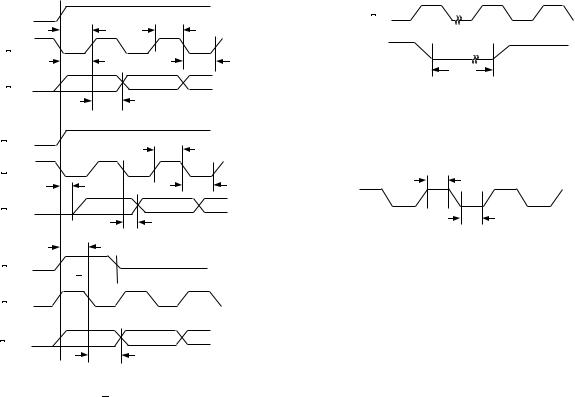
TIMING DIAGRAMS
LRCLK_I |
MCLK I |
|
|
||
tLRIS |
tSIH |
|
SCLK I |
RESET |
|
tDIS |
||
tSIL |
||
|
tRSTL |
|
SDATA I |
|
tDIH
LRCLK O
tSOH
Figure 2. RESET Timing
SCLK O |
tMPWH |
t |
tSOL |
DOPD |
|
SDATA O
tDOH
tMPWL
tLROS
Figure 3. MCLK_I Timing
LRCLK O
 tLROH
tLROH 
SCLK O
 tTDMS
tTDMS 
TDM IN
tTDMH
Figure 1. Input and Output Serial Port Timing (SCLK I/O,
LRCLK I/O, SDATA I/O, TDM IN) MacshbM
–4– |
REV. A |
|
|
|
|
AD1896 |
|
DIGITAL FILTERS (VDD_CORE = 3.3 V 5%, VDD_IO = 5.0 V 10%) |
|
|
|
||
|
|
|
|
|
|
Parameter |
Min |
Typ |
Max |
Unit |
|
|
|
|
|
|
|
Pass-Band |
|
|
0.4535 fS_OUT |
Hz |
|
Pass-Band Ripple |
|
|
±0.016 |
dB |
|
Transition Band |
0.4535 fS_OUT |
|
0.5465 fS_OUT |
Hz |
|
Stop-Band |
0.5465 fS_OUT |
|
|
Hz |
|
Stop-Band Attenuation |
|
–125 |
|
dB |
|
Group Delay |
Refer to the Group Delay Equations section. |
|
|
||
|
|
|
|
|
|
Specifications subject to change without notice. |
|
|
|
|
|
DIGITAL I/O CHARACTERISTICS (VDD_CORE = 3.3 V 5%, VDD_IO = 5.0 V |
10%) |
|
|
||
|
|
|
|
|
|
Parameter |
Min |
Typ |
Max |
Unit |
|
|
|
|
|
|
|
Input Voltage High (VIH) |
2.4 |
|
|
|
|
Input Voltage Low (VIL) |
|
|
0.8 |
V |
|
Input Leakage (IIH @ VIH = 5 V)1 |
|
|
+2 |
μA |
|
Input Leakage (IIL @ VIL = 0 V)1 |
|
|
–2 |
μA |
|
Input Leakage (IIH @ VIH = 5 V)2 |
|
|
+150 |
μA |
|
Input Leakage (IIL @ VIL = 0 V)2 |
|
|
–150 |
μA |
|
Input Capacitance |
|
5 |
10 |
pF |
|
Output Voltage High (VOH @ IOH = –4 mA) |
VDD_CORE – 0.5 |
VDD_CORE – 0.4 |
V |
||
Output Voltage Low (VOL @ IOL = +4 mA) |
|
0.2 |
0.5 |
V |
|
Output Source Current High (IOH) |
|
|
–4 |
mA |
|
Output Sink Current Low (IOL) |
|
|
+4 |
mA |
|
NOTES
1All input pins except GRPDLYS. MacshbM GRPDLYS pin only.
Specifications2 subject to change without notice.
POWER SUPPLIES
Parameter |
Min |
Typ |
Max |
Unit |
|
|
|
|
|
Supply Voltage |
|
|
|
|
VDD_CORE |
3.135 |
3.3 |
3.465 |
V |
VDD_IO* |
VDD_CORE |
3.3/5.0 |
5.5 |
V |
Active Supply Current |
|
|
|
|
I_CORE_ACTIVE |
|
|
|
|
48 kHz:48 kHz |
|
20 |
|
mA |
96 kHz:96 kHz |
|
26 |
|
mA |
192 kHz:192 kHz |
|
43 |
|
mA |
I_IO_ACTIVE |
|
2 |
|
mA |
Power-Down Supply Current: (All Clocks Stopped) |
|
|
|
|
I_CORE_PWRDN |
|
0.5 |
|
mA |
I_IO_PWRDN |
|
10 |
|
μA |
*For 3.3 V tolerant inputs, VDD_IO supply should be set to 3.3 V; however, VDD_CORE supply voltage should not exceed VDD_IO.
Specifications subject to change without notice.
REV. A |
–5– |

AD1896
POWER SUPPLIES (VDD_CORE = 3.3 V 5%, VDD_IO = 5.0 V 10%)
|
Parameter |
|
|
Min |
|
Typ |
Max |
|
Unit |
|
||||
|
|
|
|
|
|
|
|
|
|
|
|
|
|
|
|
Total Active Power Dissipation |
|
|
|
|
|
|
|
|
|
|
|
|
|
|
48 kHz:48 kHz |
|
|
|
65 |
|
|
|
|
mW |
||||
|
96 kHz:96 kHz |
|
|
|
85 |
|
|
|
|
mW |
||||
|
192 kHz:192 kHz |
|
|
|
132 |
|
|
|
|
mW |
||||
|
Total Power-Down Dissipation: (RESET LO) |
|
|
2 |
|
|
|
|
mW |
|||||
|
|
|
|
|
|
|
|
|
|
|
|
|
||
|
Specifications subject to change without notice. |
|
|
|
|
|
|
|
|
|
|
|||
|
TEMPERATURE RANGE |
|
|
|
|
|
|
|
|
|
|
|
|
|
|
|
|
|
|
|
|
|
|
|
|
|
|||
|
Parameter |
|
|
Min |
|
Typ |
Max |
|
Unit |
|||||
|
|
|
|
|
|
|
|
|
|
|
|
|||
|
Specifications Guaranteed |
|
|
|
25 |
|
|
|
|
∞C |
||||
|
Functionality Guaranteed |
|
|
–40 |
|
|
+105 |
|
|
∞C |
||||
|
Storage |
|
|
–55 |
|
|
+150 |
|
|
∞C |
||||
|
Thermal Resistance, θJA (Junction to Ambient) |
|
|
109 |
|
|
|
|
∞C/W |
|||||
|
Specifications subject to change without notice. |
|
|
|
|
|
|
|
|
|
|
|||
|
ABSOLUTE MAXIMUM RATINGS* |
|
|
|
|
|
|
|
|
|
|
|||
|
|
|
|
|
|
|
|
|
|
|
|
|
|
|
|
Parameter |
|
|
|
|
Min |
Max |
Unit |
||||||
|
|
|
|
|
|
|
|
|
|
|
|
|
|
|
|
Power Supplies |
|
|
|
|
|
|
|
|
|
|
|
|
|
|
VDD_CORE |
|
|
|
|
–0.3 |
+3.6 |
|
|
V |
||||
|
VDD_IO |
|
|
|
|
–0.3 |
+6.0 |
|
|
V |
||||
|
Digital Inputs |
|
|
|
|
|
±10 |
|
|
|
|
|
||
|
Input Current |
|
|
|
|
|
|
|
mA |
|||||
|
Input Voltage |
|
|
|
|
DGND – 0.3 |
VDD_IO + 0.3 |
V |
||||||
|
|
MacshbM |
∞C |
|
||||||||||
|
Ambient Temperature (Operating) |
|
|
–40 |
+105 |
|
|
|||||||
|
*Stresses greater than those listed under Absolute Maximum Ratings may cause perm nent d m ge to the devi e. This is tre |
rating only; functional operation of the |
||||||||||||
|
device at these or any other conditions above those indicated in the operational section of this specifi ation is not implied. Expo ure to absolute maximum rating conditions |
|||||||||||||
|
for extended periods may affect device reliability. |
|
|
|
|
|
|
|
|
|
|
|||
|
|
|
|
ORDERING GUIDE |
|
|
|
|
|
|
|
|||
|
|
|
|
|
|
|
|
|
|
|
|
|||
Model |
|
Temperature Range |
|
Package Description |
|
Package Option |
||||||||
|
|
|
|
|
|
|
|
|
|
|
|
|
|
|
AD1896AYRS |
|
–40∞C to +105∞C |
|
28-Lead SSOP |
|
RS-28 |
|
|
|
|||||
AD1896AYRSRL |
|
–40∞C to +105∞C |
|
28-Lead SSOP |
|
RS-28 on 13" Reel |
|
|||||||
CAUTION
ESD (electrostatic discharge) sensitive device. Electrostatic charges as high as 4000 V readily accumulate on the human body and test equipment and can discharge without detection. Although the AD1896 features proprietary ESD protection circuitry, permanent damage may occur on devices subjected to high-energy electrostatic discharges. Therefore, proper ESD precautions are recommended to avoid performance degradation or loss of functionality.
WARNING!
ESD SENSITIVE DEVICE
–6– |
REV. A |

AD1896
PIN CONFIGURATION
GRPDLYS |
|
|
|
MMODE_2 |
1 |
|
28 |
||
MCLK_IN |
|
|
|
MMODE_1 |
2 |
|
27 |
||
MCLK_OUT |
|
|
|
MMODE_0 |
3 |
|
26 |
||
SDATA_I |
|
AD1896 |
|
SCLK_O |
4 |
25 |
|||
SCLK_I |
|
TOP VIEW |
|
|
5 |
(NOT TO SCALE) |
24 |
LRCLK_O |
|
LRCLK_I |
|
|
SDATA_O |
|
6 |
|
23 |
||
VDD_IO |
|
|
|
VDD_CORE |
7 |
|
22 |
||
DGND |
|
|
|
DGND |
8 |
|
21 |
||
BYPASS |
|
|
|
TDM_IN |
9 |
|
20 |
||
|
|
|
|
|
SMODE_IN_0 |
10 |
|
19 |
SMODE_OUT_0 |
|
|
|
|
|
SMODE_IN_1 |
11 |
|
18 |
SMODE_OUT_1 |
|
|
|
|
|
SMODE_IN_2 |
12 |
|
17 |
WLNGTH_OUT_0 |
|
|
|
|
WLNGTH_OUT_1 |
RESET |
13 |
|
16 |
|
|
|
|
|
|
MUTE_IN |
14 |
|
15 |
MUTE_OUT |
|
|
|
|
|
|
|
|
PIN FUNCTION DESCRIPTIONS |
||
|
|
|
|
|
|
Pin No. |
|
IN/OUT |
Mnemonic |
Description |
|
|
|
|
|
|
|
1 |
|
IN |
GRPDLYS |
Group Delay High = Short, Low = Long |
|
2 |
|
|
MacshbM |
||
|
IN |
MCLK IN |
ster Clock or Crystal Input |
||
3 |
|
OUT |
MCLK OUT |
M ster Clock Output or Cry tal Output |
|
4 |
|
IN |
SDATA I |
Input Seri l Data (at Input Sample Rate) |
|
5 |
|
IN/OUT |
SCLK_I |
Master/Slave Input Serial Bit Clock |
|
6 |
|
IN/OUT |
LRCLK_I |
Master/Slave Input Left/Right Clock |
|
7 |
|
IN |
VDD_IO |
3.3 V/5 V Input/Output Digital Supply Pin |
|
8 |
|
IN |
DGND |
Digital Ground Pin |
|
9 |
|
IN |
BYPASS |
ASRC Bypass Mode, Active High |
|
10 |
|
IN |
SMODE_IN_0 |
Input Port Serial Interface Mode Select Pin 0 |
|
11 |
|
IN |
SMODE_IN_1 |
Input Port Serial Interface Mode Select Pin 1 |
|
12 |
|
IN |
SMODE_IN_2 |
Input Port Serial Interface Mode Select Pin 2 |
|
13 |
|
IN |
RESET |
Reset Pin, Active Low |
|
14 |
|
IN |
MUTE_IN |
Mute Input Pin—Active High Normally Connected to MUTE_OUT |
|
15 |
|
OUT |
MUTE_OUT |
Output Mute Control, Active High |
|
16 |
|
IN |
WLNGTH_OUT_1 |
Hardware Selectable Output Wordlength—Select Pin 1 |
|
17 |
|
IN |
WLNGTH_OUT_0 |
Hardware Selectable Output Wordlength—Select Pin 0 |
|
18 |
|
IN |
SMODE_OUT_1 |
Output Port Serial Interface Mode Select Pin 1 |
|
19 |
|
IN |
SMODE_OUT_0 |
Output Port Serial Interface Mode Select Pin 0 |
|
20 |
|
IN |
TDM_IN |
Serial Data Input* (Only for Daisy-Chain Mode). Ground when not used. |
|
21 |
|
IN |
DGND |
Digital Ground Pin |
|
22 |
|
IN |
VDD_CORE |
3.3 V Digital Supply Pin |
|
23 |
|
OUT |
SDATA_O |
Output Serial Data (at Output Sample Rate) |
|
24 |
|
IN/OUT |
LRCLK_O |
Master/Slave Output Left/Right Clock |
|
25 |
|
IN/OUT |
SCLK_O |
Master/Slave Output Serial Bit Clock |
|
26 |
|
IN |
MMODE_0 |
Master/Slave Clock Ratio Mode Select Pin 0 |
|
27 |
|
IN |
MMODE_1 |
Master/Slave Clock Ratio Mode Select Pin 1 |
|
28 |
|
IN |
MMODE_2 |
Master/Slave Clock Ratio Mode Select Pin 2 |
|
|
|
|
|
|
|
*Also used to input matched-phase mode data.
REV. A |
–7– |
AD1896–Typical Performance Characteristics
|
0 |
|
|
|
|
|
|
|
|
|
–20 |
|
|
|
|
|
|
|
|
|
–40 |
|
|
|
|
|
|
|
|
|
–60 |
|
|
|
|
|
|
|
|
|
–80 |
|
|
|
|
|
|
|
|
dBFS |
–100 |
|
|
|
|
|
|
|
|
|
|
|
|
|
|
|
|
|
|
|
–120 |
|
|
|
|
|
|
|
|
|
–140 |
|
|
|
|
|
|
|
|
|
–160 |
|
|
|
|
|
|
|
|
|
–180 |
|
|
|
|
|
|
|
|
|
–200 |
|
|
|
|
|
|
|
|
|
2.5 |
5.0 |
7.5 |
10.0 |
12.5 |
15.0 |
17.5 |
20.0 |
22.5 |
FREQUENCY – kHz
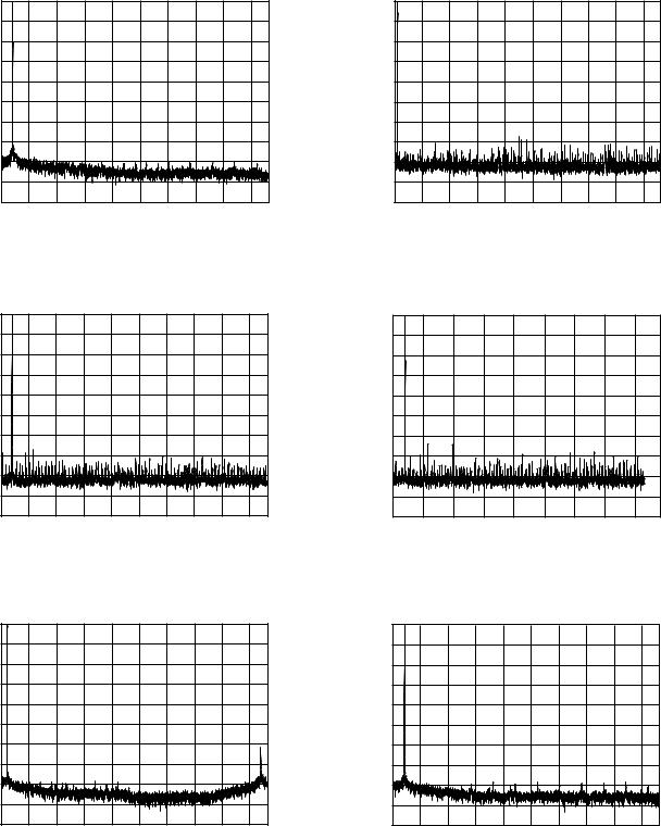
TPC 1. Wideband FFT Plot (16k Points) 0 dBFS 1 kHz Tone, 48 kHz:48 kHz (Asynchronous)
|
0 |
|
|
|
|
|
|
|
|
|
–20 |
|
|
|
|
|
|
|
|
|
–40 |
|
|
|
|
|
|
|
|
|
–60 |
|
|
|
|
|
|
|
|
|
–80 |
|
|
|
|
|
|
|
|
dBFS |
–100 |
|
|
|
|
|
|
|
|
|
|
|
|
|
|
|
|
|
|
|
–120 |
|
|
|
|
|
|
|
|
|
–140 |
|
|
|
|
|
|
|
|
|
–160 |
|
|
|
|
|
|
|
|
|
–180 |
|
|
|
|
|
|
|
|
|
–200 |
|
|
|
|
|
|
|
|
|
10 |
20 |
30 |
40 |
50 |
60 |
70 |
80 |
90 |
FREQUENCY – kHz
TPC 4. Wideband FFT Plot (16k Points) 44.1 kHz:192 kHz, 0 dBFS 1 kHz Tone
|
0 |
|
|
|
|
|
|
|
|
|
|
0 |
|
|
|
|
|
|
|
|
–20 |
|
|
|
|
|
|
|
|
|
|
–20 |
|
|
|
|
|
|
|
|
–40 |
|
|
|
|
|
|
|
|
|
|
–40 |
|
|
|
|
|
|
|
|
–60 |
|
|
|
|
|
|
|
|
|
|
–60 |
|
|
|
|
|
|
|
|
–80 |
|
|
|
|
|
|
|
|
|
|
–80 |
|
|
|
|
|
|
|
dBFS |
–100 |
|
|
|
|
|
|
|
|
|
dBFS |
–100 |
|
|
|
|
|
|
|
–120 |
|
|
|
|
|
|
|
|
|
–120 |
|
|
|
|
|
|
|
||
|
|
|
|
|
|
|
|
|
|
|
|
|
|
|
|
|
|
||
|
–140 |
|
|
|
|
|
|
|
|
|
|
–140 |
|
|
|
|
|
|
|
|
–160 |
|
|
|
|
|
|
|
|
|
|
–160 |
|
|
|
|
|
|
|
|
–180 |
MacshbM–180 |
|||||||||||||||||
|
–200 |
2.5 |
5.0 |
7.5 |
10.0 |
12.5 |
15.0 |
17.5 |
20.0 |
22.5 |
|
–200 |
|
|
|
|
|
|
|
|
|
|
2.5 |
5.0 |
7.5 |
10.0 |
12.5 |
15.0 |
17.5 |
20.0 |
|||||||||
FREQUENCY – kHz |
FREQUENCY – kHz |
TPC 2. Wideband FFT Plot (16k Points) 0 dBFS 1 kHz Tone, |
TPC 5. Wideband FFT Plot (16k Points) 48 kHz:44.1 kHz, |
44.1 kHz:48 kHz (Asynchronous) |
0 dBFS 1 kHz Tone |
|
0 |
|
|
|
|
|
|
|
|
|
–20 |
|
|
|
|
|
|
|
|
|
–40 |
|
|
|
|
|
|
|
|
|
–60 |
|
|
|
|
|
|
|
|
|
–80 |
|
|
|
|
|
|
|
|
dBFS |
–100 |
|
|
|
|
|
|
|
|
|
|
|
|
|
|
|
|
|
|
|
–120 |
|
|
|
|
|
|
|
|
|
–140 |
|
|
|
|
|
|
|
|
|
–160 |
|
|
|
|
|
|
|
|
|
–180 |
|
|
|
|
|
|
|
|
|
–200 |
|
|
|
|
|
|
|
|
|
5 |
10 |
15 |
20 |
25 |
30 |
35 |
40 |
45 |
FREQUENCY – kHz
TPC 3. Wideband FFT Plot (16k Points) 48 kHz:96 kHz, 0 dBFS 1 kHz Tone
|
0 |
|
|
|
|
|
|
|
|
|
–20 |
|
|
|
|
|
|
|
|
|
–40 |
|
|
|
|
|
|
|
|
|
–60 |
|
|
|
|
|
|
|
|
|
–80 |
|
|
|
|
|
|
|
|
dBFS |
–100 |
|
|
|
|
|
|
|
|
|
|
|
|
|
|
|
|
|
|
|
–120 |
|
|
|
|
|
|
|
|
|
–140 |
|
|
|
|
|
|
|
|
|
–160 |
|
|
|
|
|
|
|
|
|
–180 |
|
|
|
|
|
|
|
|
|
–200 |
|
|
|
|
|
|
|
|
|
2.5 |
5.0 |
7.5 |
10.0 |
12.5 |
15.0 |
17.5 |
20.0 |
22.5 |
FREQUENCY – kHz
TPC 6. Wideband FFT Plot (16k Points) 96 kHz:48 kHz, 0 dBFS 1 kHz Tone
–8– |
REV. A |

|
|
|
|
|
|
|
|
|
|
|
|
|
|
|
|
|
|
AD1896 |
|
|
0 |
|
|
|
|
|
|
|
|
|
–50 |
|
|
|
|
|
|
|
|
|
–20 |
|
|
|
|
|
|
|
|
|
–60 |
|
|
|
|
|
|
|
|
|
|
|
|
|
|
|
|
|
|
–70 |
|
|
|
|
|
|
|
|
|
|
|
|
|
|
|
|
|
|
|
|
|
|
|
|
|
|
|
|
|
|
–40 |
|
|
|
|
|
|
|
|
|
–80 |
|
|
|
|
|
|
|
|
|
–60 |
|
|
|
|
|
|
|
|
|
–90 |
|
|
|
|
|
|
|
|
|
|
|
|
|
|
|
|
|
|
–100 |
|
|
|
|
|
|
|
|
|
|
|
|
|
|
|
|
|
|
|
|
|
|
|
|
|
|
|
|
|
|
–80 |
|
|
|
|
|
|
|
|
|
–110 |
|
|
|
|
|
|
|
|
dBFS |
–100 |
|
|
|
|
|
|
|
|
dBFS |
–120 |
|
|
|
|
|
|
|
|
|
|
|
|
|
|
|
|
–130 |
|
|
|
|
|
|
|
|
|||
–120 |
|
|
|
|
|
|
|
|
|
|
|
|
|
|
|
|
|||
|
|
|
|
|
|
|
|
|
|
–140 |
|
|
|
|
|
|
|
|
|
|
–140 |
|
|
|
|
|
|
|
|
|
–150 |
|
|
|
|
|
|
|
|
|
|
|
|
|
|
|
|
|
|
–160 |
|
|
|
|
|
|
|
|
|
|
|
|
|
|
|
|
|
|
|
|
|
|
|
|
|
|
|
|
|
|
–160 |
|
|
|
|
|
|
|
|
|
–170 |
|
|
|
|
|
|
|
|
|
–180 |
|
|
|
|
|
|
|
|
|
–180 |
|
|
|
|
|
|
|
|
|
|
|
|
|
|
|
|
|
|
–190 |
|
|
|
|
|
|
|
|
|
|
|
|
|
|
|
|
|
|
|
|
|
|
|
|
|
|
|
|
|
|
–200 |
|
|
|
|
|
|
|
|
|
–200 |
|
|
|
|
|
|
|
|
|
2.5 |
5.0 |
7.5 |
10.0 |
12.5 |
15.0 |
17.5 |
20.0 |
22.5 |
|
5 |
10 |
15 |
20 |
25 |
30 |
35 |
40 |
45 |
FREQUENCY – kHz |
FREQUENCY – kHz |
|
|
TPC 7. Wideband FFT Plot (16k Points) 192 kHz:48 kHz, |
TPC 10. Wideband FFT Plot (16k Points) 48 kHz:96 kHz, |
0 dBFS 1 kHz Tone |
–60 dBFS 1 kHz Tone |
|
–50 |
|
|
|
|
|
|
|
|
|
–50 |
|
|
|
|
|
|
|
|
|
–60 |
|
|
|
|
|
|
|
|
|
–60 |
|
|
|
|
|
|
|
|
|
–70 |
|
|
|
|
|
|
|
|
|
–70 |
|
|
|
|
|
|
|
|
|
–80 |
|
|
|
|
|
|
|
|
|
–80 |
|
|
|
|
|
|
|
|
|
–90 |
|
|
|
|
|
|
|
|
|
–90 |
|
|
|
|
|
|
|
|
|
–100 |
|
|
|
|
|
|
|
|
|
–100 |
|
|
|
|
|
|
|
|
|
–110 |
|
|
|
|
|
|
|
|
dBFS |
–110 |
|
|
|
|
|
|
|
|
dBFS |
–120 |
|
|
|
|
|
|
|
|
–120 |
|
|
|
|
|
|
|
|
|
–130 |
|
|
|
|
|
|
|
|
–130 |
|
|
|
|
|
|
|
|
||
|
–140 |
|
|
|
|
|
|
|
|
|
–140 |
|
|
|
|
|
|
|
|
|
–150 |
|
|
|
|
|
|
|
|
|
–150 |
|
|
|
|
|
|
|
|
|
–160 |
|
|
|
|
|
|
|
|
|
–160 |
|
|
|
|
|
|
|
|
|
–170 |
|
|
|
|
|
|
|
|
|
–170 |
|
|
|
|
|
|
|
|
|
–180 |
|
|
|
|
|
|
|
|
|
–180 |
|
|
|
|
|
|
|
|
|
MacshbM |
||||||||||||||||||
|
–190 |
|
|
|
|
|
|
|
|
|
–190 |
|
|
|
|
|
|
|
|
|
–200 |
|
|
|
|
|
|
|
|
|
–200 |
|
|
|
|
|
|
|
|
|
2.5 |
5.0 |
7.5 |
10.0 |
12.5 |
15.0 |
17.5 |
20.0 |
22.5 |
|
10 |
20 |
30 |
40 |
50 |
60 |
70 |
80 |
90 |
FREQUENCY – kHz |
FREQUENCY – kHz |
TPC 8. Wideband FFT Plot (16k Points) –60 dBFS 1 kHz |
TPC 11. Wideband FFT Plot (16k Points) 44.1 kHz:192 kHz, |
Tone, 48 kHz:48 kHz (Asynchronous) |
–60 dBFS 1 kHz Tone |
|
–50 |
|
|
|
|
|
|
|
|
|
–60 |
|
|
|
|
|
|
|
|
|
–70 |
|
|
|
|
|
|
|
|
|
–80 |
|
|
|
|
|
|
|
|
|
–90 |
|
|
|
|
|
|
|
|
|
–100 |
|
|
|
|
|
|
|
|
|
–110 |
|
|
|
|
|
|
|
|
dBFS |
–120 |
|
|
|
|
|
|
|
|
–130 |
|
|
|
|
|
|
|
|
|
–140 |
|
|
|
|
|
|
|
|
|
|
|
|
|
|
|
|
|
|
|
|
–150 |
|
|
|
|
|
|
|
|
|
–160 |
|
|
|
|
|
|
|
|
|
–170 |
|
|
|
|
|
|
|
|
|
–180 |
|
|
|
|
|
|
|
|
|
–190 |
|
|
|
|
|
|
|
|
|
–200 |
|
|
|
|
|
|
|
|
|
2.5 |
5.0 |
7.5 |
10.0 |
12.5 |
15.0 |
17.5 |
20.0 |
22.5 |
FREQUENCY – kHz
TPC 9. Wideband FFT Plot (16k Points) 44.1 kHz:48 kHz, –60 dBFS 1 kHz Tone
–50 |
|
|
|
|
|
|
|
–60 |
|
|
|
|
|
|
|
–70 |
|
|
|
|
|
|
|
–80 |
|
|
|
|
|
|
|
–90 |
|
|
|
|
|
|
|
–100 |
|
|
|
|
|
|
|
–110 |
|
|
|
|
|
|
|
–120 |
|
|
|
|
|
|
|
dBFS –130 |
|
|
|
|
|
|
|
–140 |
|
|
|
|
|
|
|
–150 |
|
|
|
|
|
|
|
–160 |
|
|
|
|
|
|
|
–170 |
|
|
|
|
|
|
|
–180 |
|
|
|
|
|
|
|
–190 |
|
|
|
|
|
|
|
–200 |
|
|
|
|
|
|
|
2.5 |
5.0 |
7.5 |
10.0 |
12.5 |
15.0 |
17.5 |
20.0 |
FREQUENCY – kHz
TPC 12. Wideband FFT Plot (16k Points) 48 kHz:44.1 kHz, –60 dBFS 1 kHz Tone
REV. A |
–9– |
Loading...