


 Loading...
|
Nonvolatile Memory, Dual |
|
1024-Position Digital Potentiometer |
Data Sheet |
AD5235 |
|
|
FEATURES
Dual-channel, 1024-position resolution 25 kΩ, 250 kΩ nominal resistance
Maximum ±8% nominal resistor tolerance error Low temperature coefficient: 35 ppm/°C
2.7 V to 5 V single supply or ±2.5 V dual supply SPI-compatible serial interface
Nonvolatile memory stores wiper settings Power-on refreshed with EEMEM settings Permanent memory write protection Resistance tolerance stored in EEMEM
26 bytes extra nonvolatile memory for user-defined information
1M programming cycles
100-year typical data retention
APPLICATIONS
DWDM laser diode driver, optical supervisory systems Mechanical potentiometer replacement Instrumentation: gain, offset adjustment Programmable voltage-to-current conversion Programmable filters, delays, time constants Programmable power supply
Low resolution DAC replacement Sensor calibration
GENERAL DESCRIPTION
The AD5235 is a dual-channel, nonvolatile memory,1 digitally controlled potentiometer2 with 1024-step resolution, offering guaranteed maximum low resistor tolerance error of ±8%.
The device performs the same electronic adjustment function as a mechanical potentiometer with enhanced resolution, solid state reliability, and superior low temperature coefficient performance. The versatile programming of the AD5235 via an SPI®-compatible serial interface allows 16 modes of operation and adjustment including scratchpad programming, memory storing and restoring, increment/decrement, ±6 dB/step log taper adjustment, wiper setting readback, and extra EEMEM1 for user-
defined information such as memory data for other components, look-up table, or system identification information.
1The terms nonvolatile memory and EEMEM are used interchangeably.
2The terms digital potentiometer and RDAC are used interchangeably.
Rev. F
Information furnished by Analog Devices is believed to be accurate and reliable. However, no responsibilityisassumedbyAnalogDevicesforitsuse,norforanyinfringementsofpatentsorother rightsofthirdpartiesthatmayresultfromitsuse.Specificationssubjecttochangewithoutnotice.No license isgranted by implication or otherwise under any patent or patent rightsof Analog Devices. Trademarksandregisteredtrademarksarethepropertyoftheirrespectiveowners.
FUNCTIONAL BLOCK DIAGRAM
|
ADDR |
|
RDAC1 |
AD5235 |
VDD |
CS |
DECODE |
|
|
|
|
CLK |
|
|
REGISTER |
|
A1 |
|
|
|
|
||
SERIAL |
|
|
|
W1 |
|
SDI |
|
|
|
||
|
|
|
|
||
INTERFACE |
|
|
|
B1 |
|
SDO |
|
EEMEM1 |
RDAC1 |
||
|
|
|
|||
PR |
POWER-ON |
|
|
|
|
RESET |
|
RDAC2 |
|
|
|
|
|
|
|
||
|
|
|
|
A2 |
|
WP |
EEMEM |
|
REGISTER |
|
|
|
|
|
W2 |
||
RDY |
CONTROL |
|
|
|
B2 |
|
|
|
EEMEM2 |
RDAC2 |
|
|
|
|
|
||
|
|
|
|
|
|
|
|
|
26 BYTES |
|
VSS |
|
|
RTOL* |
|
|
|
|
|
USER EEMEM |
|
|
|
|
|
|
|
GND |
|
|
|
|
|
|
|
*RAB TOLERANCE |
|
|
|
02816-001 |
|
Figure 1.
In the scratchpad programming mode, a specific setting can be programmed directly to the RDAC2 register, which sets the resistance between Terminal W and Terminal A and Terminal W and Terminal B. This setting can be stored into the EEMEM and is restored automatically to the RDAC register during system power-on.
The EEMEM content can be restored dynamically or through external PR strobing, and a WP function protects EEMEM contents. To simplify the programming, the independent or simultaneous linear-step increment or decrement commands can be used to move the RDAC wiper up or down, one step at a time. For logarithmic ±6 dB changes in the wiper setting, the left or right bit shift command can be used to double or halve the RDAC wiper setting.
The AD5235 patterned resistance tolerance is stored in the EEMEM. The actual end-to-end resistance can, therefore, be known by the host processor in readback mode. The host can execute the appropriate resistance step through a software routine that simplifies open-loop applications as well as precision calibration and tolerance matching applications.
The AD5235 is available in a thin, 16-lead TSSOP package. The part is guaranteed to operate over the extended industrial temperature range of −40°C to +85°C.
One Technology Way, P.O. Box 9106, Norwood, MA 02062-9106, U.S.A. Tel: 781.329.4700 www.analog.com Fax: 781.461.3113 ©2004–2012 Analog Devices, Inc. All rights reserved.

AD5235 |
Data Sheet |
TABLE OF CONTENTS |
|
Features .............................................................................................. |
1 |
Applications....................................................................................... |
1 |
General Description ......................................................................... |
1 |
Functional Block Diagram .............................................................. |
1 |
Revision History ............................................................................... |
3 |
Specifications..................................................................................... |
4 |
Electrical Characteristics—25 kΩ, 250 kΩ Versions ............... |
4 |
Interface Timing and EEMEM Reliability Characteristics— |
|
25 kΩ, 250 kΩ Versions ............................................................... |
6 |
Absolute Maximum Ratings............................................................ |
8 |
ESD Caution.................................................................................. |
8 |
Pin Configuration and Function Descriptions............................. |
9 |
Typical Performance Characteristics ........................................... |
10 |
Test Circuits................................................................................. |
14 |
Theory of Operation ...................................................................... |
16 |
Scratchpad and EEMEM Programming.................................. |
16 |
Basic Operation .......................................................................... |
16 |
EEMEM Protection.................................................................... |
17 |
Digital Input and Output Configuration................................. |
17 |
Serial Data Interface................................................................... |
17 |
Daisy-Chain Operation ............................................................. |
18 |
Terminal Voltage Operating Range.......................................... |
18 |
Advanced Control Modes ......................................................... |
20 |
RDAC Structure.......................................................................... |
21 |
Programming the Variable Resistor......................................... |
22 |
Programming the Potentiometer Divider............................... |
22 |
Programming Examples ............................................................ |
23 |
EVAL-AD5235SDZ Evaluation Kit.......................................... |
23 |
Applications Information .............................................................. |
24 |
Bipolar Operation from Dual Supplies.................................... |
24 |
Gain Control Compensation .................................................... |
24 |
High Voltage Operation ............................................................ |
24 |
DAC.............................................................................................. |
24 |
Bipolar Programmable Gain Amplifier................................... |
25 |
10-Bit Bipolar DAC.................................................................... |
25 |
Programmable Voltage Source with Boosted Output ........... |
25 |
Programmable Current Source ................................................ |
26 |
Programmable Bidirectional Current Source......................... |
26 |
Programmable Low-Pass Filter ................................................ |
27 |
Programmable Oscillator .......................................................... |
27 |
Optical Transmitter Calibration with ADN2841 ................... |
28 |
Resistance Scaling ...................................................................... |
28 |
Resistance Tolerance, Drift, and Temperature Coefficient |
|
Mismatch Considerations ......................................................... |
29 |
RDAC Circuit Simulation Model............................................. |
29 |
Outline Dimensions ....................................................................... |
30 |
Ordering Guide .......................................................................... |
30 |
Rev. F | Page 2 of 32
Data Sheet |
AD5235 |
|
|
REVISION HISTORY |
|
|
6/12—Rev. E to Rev. F |
|
|
Changes to Table 1 Conditions........................................................ |
|
4 |
Removed Positive Supply Current RDY and/or SDO Floating |
|
|
Parameters and Negative Supply Current RDY and/or SDO |
|
|
Floating Parameters, Table 1............................................................ |
|
5 |
Added Endnote 2 to Ordering Guide ........................................... |
|
30 |
4/11—Rev. D to Rev. E |
|
|
Changes to Figure 12 ...................................................................... |
|
11 |
4/11—Rev. C to Rev. D |
|
|
Changes to EEMEM Performance .............................. |
Throughout |
|
Changes to Features and General Descriptions Sections............. |
1 |
|
Changes to Specifications Section................................................... |
|
4 |
Changes to Pin 5, Pin 13, Pin 14 Descriptions.............................. |
|
9 |
Changes to Typical Performance Characteristics Section ......... |
10 |
|
Changes to Table 7 .......................................................................... |
|
19 |
Changes to Table 9 .......................................................................... |
|
21 |
Changes to Rheostat Operation Section, Table 12, Table 13 ..... |
22 |
|
Changes to Table 16, Table 19, and EVAL-AD5235SDZ |
|
|
Evaluation Kit Section .................................................................... |
|
23 |
Changes to RDAC Circuit Simulation Model Section ............... |
29 |
|
Updated Outline Dimensions........................................................ |
|
30 |
Changes to Ordering Guide........................................................... |
|
30 |
4/09—Rev. B to Rev. C |
|
|
Changes to Figure 1........................................................................... |
|
1 |
Changes to Specifications................................................................. |
|
3 |
Changes to SDO, Description Column, Table 4............................ |
|
8 |
Changes to Figure 18 ...................................................................... |
|
11 |
Changes to Theory of Operation Section .................................... |
|
14 |
Changes to Serial Data Interface Section..................................... |
|
15 |
Changes to Linear Increment and Decrement Instructions |
|
|
Section, Logarithmic Taper Mode Adjustment Section, and |
|
|
Figure 42 ........................................................................................... |
|
18 |
Changes to Rheostat Operations Section..................................... |
|
20 |
Changes to Bipolar Programmable Gain Amplifier Section, |
|
|
Figure 49, Table 21, and 10-Bit Bipolar DAC Section ................ |
23 |
|
Changes to Programmable Oscillator Section and Figure 56 ... |
25 |
|
Changes to Ordering Guide........................................................... |
|
28 |
7/04—Rev. A to Rev. B |
|
|
Updated Formatting .......................................................... |
Universal |
|
Edits to Features, General Description, and Block Diagram |
......1 |
|
Changes to Specifications................................................................. |
|
3 |
Replaced Timing Diagrams ............................................................. |
|
6 |
Changes to Absolute Maximum Ratings........................................ |
|
7 |
Changes to Pin Function Descriptions .......................................... |
|
8 |
Changes to Typical Performance Characteristics ......................... |
|
9 |
Additional Test Circuit (Figure 36)................................................. |
|
9 |
Edits to Theory of Operation ........................................................ |
|
14 |
Edits to Applications....................................................................... |
|
23 |
Updated Outline Dimensions........................................................ |
|
27 |
8/02—Rev. 0 to Rev. A |
|
|
Change to Features and General Description ............................... |
|
1 |
Change to Specifications .................................................................. |
|
2 |
Change to Calculating Actual End-to-End Terminal |
|
|
Resistance Section........................................................................... |
|
14 |
Rev. F | Page 3 of 32

AD5235 |
Data Sheet |
SPECIFICATIONS
ELECTRICAL CHARACTERISTICS—25 kΩ, 250 kΩ VERSIONS
VDD = 2.7 V to 5.5 V, VSS = 0 V; VDD = 2.5 V, VSS = −2.5 V, VA = VDD, VB = VSS, −40°C < TA < +85°C, unless otherwise noted. These specifications apply to versions with a date code 1209 or later.
Table 1.
Parameter |
Symbol |
Conditions |
Min |
Typ1 |
Max |
Unit |
DC CHARACTERISTICS—RHEOSTAT |
|
|
|
|
|
|
MODE (All RDACs) |
|
|
|
|
|
|
Resistor Differential Nonlinearity2 |
R-DNL |
RWB |
−1 |
|
+1 |
LSB |
Resistor Integral Nonlinearity2 |
R-INL |
RWB |
−2 |
|
+2 |
LSB |
Nominal Resistor Tolerance |
∆RAB/RAB |
|
−8 |
|
+8 |
% |
Resistance Temperature Coefficient |
(∆RAB/RAB)/∆T × 106 |
|
|
35 |
|
ppm/°C |
Wiper Resistance |
RW |
IW = 1 V/RWB, code = midscale |
|
|
|
|
|
|
VDD = 5 V |
|
30 |
60 |
Ω |
|
|
VDD = 3 V |
|
50 |
|
Ω |
Nominal Resistance Match |
RAB1/RAB2 |
|
|
±0.1 |
|
% |
|
|
|
|
|
|
|
DC CHARACTERISTICS— |
|
|
|
|
|
|
POTENTIOMETER DIVIDER MODE |
|
|
|
|
|
|
(All RDACs) |
|
|
|
|
|
|
Resolution |
N |
|
|
|
10 |
Bits |
Differential Nonlinearity3 |
DNL |
|
−1 |
|
+1 |
LSB |
Integral Nonlinearity3 |
INL |
|
−1 |
|
+1 |
LSB |
Voltage Divider Temperature |
(∆VW/VW)/∆T × 106 |
Code = midscale |
|
15 |
|
ppm/°C |
Coefficient |
|
|
|
|
|
|
Full-Scale Error |
VWFSE |
Code = full scale |
−6 |
|
0 |
LSB |
Zero-Scale Error |
VWZSE |
Code = zero scale |
0 |
|
4 |
LSB |
|
|
|
|
|
|
|
RESISTOR TERMINALS |
|
|
|
|
|
|
Terminal Voltage Range4 |
VA, VB, VW |
|
VSS |
|
VDD |
V |
Capacitance Ax, Bx5 |
CA, CB |
f = 1 MHz, measured to GND, |
|
11 |
|
pF |
|
|
code = midscale |
|
|
|
|
Capacitance Wx5 |
CW |
f = 1 MHz, measured to GND, |
|
80 |
|
pF |
|
|
code = midscale |
|
|
|
|
Common-Mode Leakage Current5, 6 |
ICM |
VW = VDD/2 |
|
0.01 |
±1 |
µA |
DIGITAL INPUTS AND OUTPUTS |
|
|
|
|
|
|
Input Logic High |
VIH |
With respect to GND, VDD = 5 V |
2.4 |
|
|
V |
Input Logic Low |
VIL |
With respect to GND, VDD = 5 V |
|
|
0.8 |
V |
Input Logic High |
VIH |
With respect to GND, VDD = 3 V |
2.1 |
|
|
V |
Input Logic Low |
VIL |
With respect to GND, VDD = 3 V |
|
|
0.6 |
V |
Input Logic High |
VIH |
With respect to GND, VDD = +2.5 V, |
2.0 |
|
|
V |
|
|
VSS = −2.5 V |
|
|
|
|
Input Logic Low |
VIL |
With respect to GND, VDD = +2.5 V, |
|
|
0.5 |
V |
|
|
VSS = −2.5 V |
|
|
|
|
Output Logic High (SDO, RDY) |
VOH |
RPULL-UP = 2.2 kΩ to 5 V (see |
4.9 |
|
|
V |
|
|
Figure 38) |
|
|
|
|
Output Logic Low |
VOL |
IOL = 1.6 mA, VLOGIC = 5 V (see |
|
|
0.4 |
V |
|
|
Figure 38) |
|
|
|
|
Input Current |
IIL |
VIN = 0 V or VDD |
|
|
±1 |
µA |
Input Capacitance5 |
CIL |
|
|
5 |
|
pF |
Rev. F | Page 4 of 32
Data Sheet |
|
|
|
|
AD5235 |
|
|
|
|
|
|
|
|
|
|
|
|
|
|
|
Parameter |
Symbol |
Conditions |
Min |
Typ1 |
Max |
Unit |
POWER SUPPLIES |
|
|
|
|
|
|
Single-Supply Power Range |
VDD |
VSS = 0 V |
2.7 |
|
5.5 |
V |
Dual-Supply Power Range |
VDD/VSS |
|
±2.25 |
|
±2.75 |
V |
Positive Supply Current |
IDD |
VIH = VDD or VIL = GND |
|
2 |
5 |
µA |
Negative Supply Current |
ISS |
VDD = +2.5 V, VSS = −2.5 V |
|
|
|
|
|
|
VIH = VDD or VIL = GND |
−4 |
−2 |
|
µA |
EEMEM Store Mode Current |
IDD (store) |
VIH = VDD or VIL = GND, |
|
2 |
|
mA |
|
|
VSS = GND, ISS ≈ 0 |
|
|
|
|
|
ISS (store) |
VDD = +2.5 V, VSS = −2.5 V |
|
−2 |
|
mA |
EEMEM Restore Mode Current7 |
IDD (restore) |
VIH = VDD or VIL = GND, |
|
320 |
|
µA |
|
|
VSS = GND, ISS ≈ 0 |
|
|
|
|
|
ISS (restore) |
VDD = +2.5 V, VSS = −2.5 V |
|
−320 |
|
µA |
Power Dissipation8 |
PDISS |
VIH = VDD or VIL = GND |
|
10 |
30 |
µW |
Power Supply Sensitivity5 |
PSS |
∆VDD = 5 V ± 10% |
|
0.006 |
0.01 |
%/% |
DYNAMIC CHARACTERISTICS5, 9 |
|
|
|
|
|
|
Bandwidth |
BW |
−3 dB, RAB = 25 kΩ/250 kΩ |
|
125/12 |
|
kHz |
Total Harmonic Distortion |
THDW |
VA = 1 V rms, VB = 0 V, |
|
|
|
|
|
|
f = 1 kHz, code = midscale |
|
|
|
|
|
|
RAB = 25 kΩ |
|
0.009 |
|
% |
|
|
RAB = 250 kΩ |
|
0.035 |
|
% |
VW Settling Time |
tS |
VA = VDD, VB = 0 V, VW = 0.50% error |
|
|
|
|
|
|
band, from zero scale to midscale |
|
|
|
|
|
|
RAB = 25 kΩ |
|
4 |
|
µs |
|
|
RAB = 250 kΩ |
|
36 |
|
µs |
Resistor Noise Density |
eN_WB |
RAB = 25 kΩ/250 kΩ |
|
20/64 |
|
nV/√Hz |
Crosstalk (CW1/CW2) |
CT |
VA1 = VDD, VB1 = VSS , measured VW2 |
|
30/60 |
|
nV-s |
|
|
with VW1 making full-scale change, |
|
|
|
|
|
|
RAB = 25 kΩ/250 kΩ |
|
|
|
|
Analog Crosstalk |
CTA |
VAB2 = 5 V p-p, f = 1 kHz, measured |
|
−110/−100 |
|
dB |
|
|
VW1, Code 1 = midscale, Code 2 = |
|
|
|
|
|
|
full scale, RAB = 25 kΩ/250 kΩ |
|
|
|
|
1Typicals represent average readings at 25°C and VDD = 5 V.
2Resistor position nonlinearity error (R-INL) is the deviation from an ideal value measured between the maximum resistance and the minimum resistance wiper positions. R-DNL measures the relative step change from ideal between successive tap positions. IWB = (VDD − 1)/RWB (see Figure 27).
3INL and DNL are measured at VW with the RDAC configured as a potentiometer divider similar to a voltage output DAC. VA = VDD and VB = VSS. DNL specification limits of ±1 LSB maximum are guaranteed monotonic operating conditions (see Figure 28).
4Resistor Terminal A, Resistor Terminal B, and Resistor Terminal W have no limitations on polarity with respect to each other. Dual-supply operation enables groundreferenced bipolar signal adjustment.
5Guaranteed by design and not subject to production test.
6Common-mode leakage current is a measure of the dc leakage from any Terminal A, Terminal B, or Terminal W to a common-mode bias level of VDD/2.
7EEMEM restore mode current is not continuous. Current is consumed while EEMEM locations are read and transferred to the RDAC register.
8PDISS is calculated from (IDD × VDD) + (ISS × VSS).
9All dynamic characteristics use VDD = +2.5 V and VSS = −2.5 V.
Rev. F | Page 5 of 32

AD5235 |
Data Sheet |
INTERFACE TIMING AND EEMEM RELIABILITY CHARACTERISTICS—25 kΩ, 250 kΩ VERSIONS
Guaranteed by design and not subject to production test. See the Timing Diagrams section for the location of measured values. All input control voltages are specified with tR = tF = 2.5 ns (10% to 90% of 3 V) and timed from a voltage level of 1.5 V. Switching characteristics are measured using both VDD = 2.7 V and VDD = 5 V.
Table 2.
|
Parameter |
Symbol |
|
Conditions |
Min |
Typ1 |
Max |
Unit |
|||||||||
|
Clock Cycle Time (tCYC) |
t1 |
|
|
|
20 |
|
|
ns |
||||||||
|
|
|
|
|
|
|
|
|
t2 |
|
|
|
10 |
|
|
ns |
|
|
CS |
Setup Time |
|
|
|
|
|
||||||||||
|
|
|
|
|
|
|
|
|
|
|
|
|
|
|
|||
|
CLK Shutdown Time to |
CS |
Rise |
t3 |
|
|
|
1 |
|
|
tCYC |
||||||
|
Input Clock Pulse Width |
t4, t5 |
|
Clock level high or low |
10 |
|
|
ns |
|||||||||
|
Data Setup Time |
t6 |
|
From positive CLK transition |
5 |
|
|
ns |
|||||||||
|
Data Hold Time |
t7 |
|
From positive CLK transition |
5 |
|
|
ns |
|||||||||
|
|
|
|
|
|
|
t8 |
|
|
|
|
|
40 |
ns |
|||
|
CS |
to SDO-SPI Line Acquire |
|
|
|
|
|
||||||||||
|
|
|
|
|
|
|
t9 |
|
|
|
|
|
50 |
ns |
|||
|
CS |
to SDO-SPI Line Release |
|
|
|
|
|
||||||||||
|
CLK to SDO Propagation Delay2 |
t10 |
|
RP = 2.2 kΩ, CL < 20 pF |
|
|
50 |
ns |
|||||||||
|
CLK to SDO Data Hold Time |
t11 |
|
RP = 2.2 kΩ, CL < 20 pF |
0 |
|
|
ns |
|||||||||
|
|
|
|
|
|
|
t12 |
|
|
|
10 |
|
|
ns |
|||
|
CS |
High Pulse Width3 |
|
|
|
|
|
||||||||||
|
|
|
|
|
High3 |
t13 |
|
|
|
4 |
|
|
tCYC |
||||
|
CS |
High to |
CS |
|
|
|
|
|
|||||||||
|
RDY Rise to |
CS |
Fall |
t14 |
|
|
|
0 |
|
|
ns |
||||||
|
|
t15 |
|
|
|
|
0.15 |
0.3 |
ms |
||||||||
|
CS |
Rise to RDY Fall Time |
|
|
|
|
|||||||||||
|
Store EEMEM Time4, 5 |
t16 |
|
Applies to Instructions 0x2, 0x3 |
|
15 |
50 |
ms |
|||||||||
|
Read EEMEM Time4 |
t16 |
|
Applies to Instructions 0x8, 0x9, 0x10 |
|
7 |
30 |
µs |
|||||||||
|
CS |
Rise to Clock Rise/Fall Setup |
t17 |
|
|
|
10 |
|
|
ns |
|||||||
|
Preset Pulse Width (Asynchronous)6 |
tPRW |
|
|
|
50 |
|
|
ns |
||||||||
|
Preset Response Time to Wiper Setting6 |
tPRESP |
|
PR |
pulsed low to refresh wiper positions |
|
30 |
|
µs |
||||||||
|
Power-On EEMEM Restore Time6 |
tEEMEM |
|
|
|
|
30 |
|
µs |
||||||||
|
FLASH/EE MEMORY RELIABILITY |
|
|
|
|
|
|
|
|
||||||||
|
Endurance7 |
|
|
TA = 25°C |
|
1 |
|
MCycles |
|||||||||
|
|
|
|
|
|
|
|
|
|
|
|
|
|
100 |
|
|
kCycles |
|
Data Retention8 |
|
|
|
|
|
100 |
|
Years |
||||||||
1Typicals represent average readings at 25°C and VDD = 5 V.
2Propagation delay depends on the value of VDD, RPULL-UP, and CL.
3Valid for commands that do not activate the RDY pin.
4The RDY pin is low only for Instruction 2, Instruction 3, Instruction 8, Instruction 9, Instruction 10, and the PR hardware pulse: CMD_8 ~ 20 µs; CMD_9, CMD_10 ~ 7 µs; CMD_2, CMD_3 ~ 15 ms; PR hardware pulse ~ 30 µs.
5Store EEMEM time depends on the temperature and EEMEM writes cycles. Higher timing is expected at a lower temperature and higher write cycles.
6Not shown in Figure 2 and Figure 3.
7Endurance is qualified to 100,000 cycles per JEDEC Standard 22, Method A117 and measured at −40°C, +25°C, and +85°C.
8Retention lifetime equivalent at junction temperature (TJ) = 85°C per JEDEC Standard 22, Method A117. Retention lifetime based on an activation energy of 1 eV derates with junction temperature in the Flash/EE memory.
Rev. F | Page 6 of 32
Data Sheet |
AD5235 |
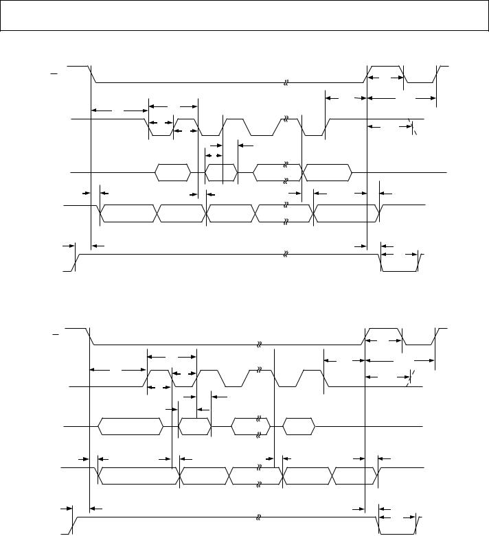
Timing Diagrams
|
|
|
CPHA = 1 |
|
|
CS |
|
|
|
|
t12 |
|
|
|
t1 |
t3 |
t13 |
|
|
t2 |
|
|
|
CLK |
|
|
|
|
|
|
t5 |
B23 |
B0 |
|
|
CPOL = 1 |
|
t17 |
|||
|
|
t4 |
|
||
|
|
|
|
|
|
|
|
|
t7 |
|
|
|
HIGH |
|
t6 |
|
|
|
|
|
|
|
|
SDI |
OR LOW |
B23 (MSB) |
B0 (LSB) |
|
|
|
|
||||
|
t8 |
|
t10 |
t11 |
t9 |
SDO |
|
B24* |
B23 (MSB) |
B0 (LSB) |
|
|
t14 |
|
|
|
t15 |
RDY |
|
|
|
|
t16 |
|
|
|
|
|
|
*THE EXTRA BIT THAT IS NOT DEFINED IS NORMALLY THE LSB OF THE CHARACTER PREVIOUSLY TRANSMITTED. THE CPOL = 1 MICROCONTROLLER COMMAND ALIGNS THE INCOMING DATA TO THE POSITIVE EDGE OF THE CLOCK.
HIGH OR LOW
02816-002
|
|
|
|
Figure 2. CPHA = 1 Timing Diagram |
|
|
|
|
|
CPHA = 0 |
|
CS |
|
|
|
|
t12 |
|
|
|
|
|
|
|
|
t1 |
|
t3 |
t13 |
|
|
t2 |
|
||
|
|
t5 |
|
t17 |
|
CLK |
|
B23 |
B0 |
||
|
|
||||
CPOL = 0 |
|
t4 |
|
t7 |
|
|
|
|
|
|
|
|
HIGH |
|
t6 |
|
HIGH |
SDI |
OR LOW |
B23 (MSB IN) |
|
B0 (LSB) |
OR LOW |
|
|
|
|||
|
t8 |
t10 |
|
t11 |
t9 |
|
|
|
|
|
|
SDO |
|
B23 (MSB OUT) |
|
B0 (LSB) |
* |
|
|
|
|
|
|
|
t14 |
|
|
|
t15 |
|
|
|
|
|
t16 |
RDY |
|
|
|
|
|
*THE EXTRA BIT THAT IS NOT DEFINED IS NORMALLY THE MSB OF THE CHARACTER JUST RECEIVED.
THE CPOL = 0 MICROCONTROLLER COMMAND ALIGNS THE INCOMING DATA TO THE POSITIVE EDGE OF THE CLOCK.
Figure 3. CPHA = 0 Timing Diagram
02816-003
Rev. F | Page 7 of 32
AD5235 |
Data Sheet |
ABSOLUTE MAXIMUM RATINGS
TA = 25°C, unless otherwise noted.
Table 3.
Parameter |
Rating |
VDD to GND |
–0.3 V to +7 V |
VSS to GND |
+0.3 V to −7 V |
VDD to VSS |
7 V |
VA, VB, VW to GND |
VSS − 0.3 V to VDD + 0.3 V |
IA, IB, IW |
|
Pulsed1 |
±20 mA |
Continuous |
±2 mA |
Digital Input and Output Voltage to GND |
−0.3 V to VDD + 0.3 V |
Operating Temperature Range2 |
−40°C to +85°C |
Maximum Junction Temperature (TJ max) |
150°C |
Storage Temperature Range |
−65°C to +150°C |
Lead Temperature, Soldering |
|
Vapor Phase (60 sec) |
215°C |
Infrared (15 sec) |
220°C |
Thermal Resistance |
|
Junction-to-Ambient θJA,TSSOP-16 |
150°C/W |
Junction-to-Case θJC, TSSOP-16 |
28°C/W |
Package Power Dissipation |
(TJ max − TA)/θJA |
1Maximum terminal current is bounded by the maximum current handling of the switches, maximum power dissipation of the package, and maximum applied voltage across any two of the A, B, and W terminals at a given resistance.
2Includes programming of nonvolatile memory.
Stresses above those listed under Absolute Maximum Ratings may cause permanent damage to the device. This is a stress rating only; functional operation of the device at these or any other conditions above those indicated in the operational section of this specification is not implied. Exposure to absolute maximum rating conditions for extended periods may affect device reliability.
ESD CAUTION
Rev. F | Page 8 of 32

Data Sheet |
AD5235 |
PIN CONFIGURATION AND FUNCTION DESCRIPTIONS
CLK |
1 |
|
16 |
RDY |
||||
SDI |
2 |
|
|
|
|
|
|
|
|
15 |
|
CS |
|||||
SDO |
|
|
|
|
|
|
||
3 |
|
14 |
|
PR |
|
|
||
GND |
|
AD5235 |
|
|
|
|||
4 |
13 |
|
WP |
|
||||
VSS |
5 |
TOP VIEW |
12 |
|
VDD |
|||
(Not to Scale) |
|
|||||||
A1 |
6 |
|
11 |
A2 |
||||
W1 |
7 |
|
10 |
W2 |
||||
B1 8
9 B2
02816-005
|
|
|
|
|
Figure 4. Pin Configuration |
||||||||
Table 4. Pin Function Descriptions |
|||||||||||||
Pin No. |
|
Mnemonic |
Description |
||||||||||
1 |
|
CLK |
Serial Input Register Clock. Shifts in one bit at a time on positive clock edges. |
||||||||||
2 |
|
SDI |
Serial Data Input. Shifts in one bit at a time on positive clock CLK edges. MSB loads first. |
||||||||||
3 |
|
SDO |
Serial Data Output. Serves readback and daisy-chain functions. Command 9 and Command 10 activate the SDO |
||||||||||
|
|
|
|
|
output for the readback function, delayed by 24 or 25 clock pulses, depending on the clock polarity before and |
||||||||
|
|
|
|
|
after the data-word (see Figure 2 and Figure 3). In other commands, the SDO shifts out the previously loaded SDI |
||||||||
|
|
|
|
|
bit pattern, delayed by 24 or 25 clock pulses depending on the clock polarity (see Figure 2 and Figure 3). This |
||||||||
|
|
|
|
|
previously shifted out SDI can be used for daisy-chaining multiple devices. Whenever SDO is used, a pull-up |
||||||||
|
|
|
|
|
resistor in the range of 1 kΩ to 10 kΩ is needed. |
||||||||
4 |
|
GND |
Ground Pin, Logic Ground Reference. |
||||||||||
5 |
|
VSS |
Negative Supply. Connect to 0 V for single-supply applications. If VSS is used in dual supply, it must be able to sink |
||||||||||
|
|
|
|
|
2 mA for 15 ms when storing data to EEMEM. |
||||||||
6 |
|
A1 |
Terminal A of RDAC1. |
||||||||||
7 |
|
W1 |
Wiper terminal of RDAC1. ADDR (RDAC1) = 0x0. |
||||||||||
8 |
|
B1 |
Terminal B of RDAC1. |
||||||||||
9 |
|
B2 |
Terminal B of RDAC2. |
||||||||||
10 |
|
W2 |
Wiper terminal of RDAC2. ADDR (RDAC2) = 0x1. |
||||||||||
11 |
|
A2 |
Terminal A of RDAC2. |
||||||||||
12 |
|
VDD |
Positive Power Supply. |
||||||||||
13 |
|
|
|
Optional Write Protect. When active low, |
|
prevents any changes to the present contents, except |
|
strobe. |
|||||
|
WP |
|
WP |
PR |
|||||||||
|
|
|
|
|
CMD_1 and COMD_8 refresh the RDAC register from EEMEM. Tie WP to VDD, if not used. |
||||||||
14 |
|
|
Optional Hardware Override Preset. Refreshes the scratchpad register with current contents of the EEMEM |
||||||||||
|
PR |
|
|||||||||||
|
|
|
|
|
register. Factory default loads midscale until EEMEM is loaded with a new value by the user. |
PR |
is activated |
||||||
|
|
|
|
|
at the logic high transition. Tie PR to VDD, if not used. |
||||||||
15 |
|
|
Serial Register Chip Select Active Low. Serial register operation takes place when |
|
returns to logic high. |
||||||||
|
CS |
|
CS |
||||||||||
16 |
|
RDY |
Ready. Active high open-drain output. Identifies completion of Instruction 2, Instruction 3, Instruction 8, |
||||||||||
|
|
|
|
|
Instruction 9, Instruction 10, and PR. |
||||||||
|
|
|
|
|
|
|
|
|
|
|
|
|
|
Rev. F | Page 9 of 32

AD5235 |
Data Sheet |
TYPICAL PERFORMANCE CHARACTERISTICS
|
0.20 |
+85°C |
|
|
|
|
|
|
|
|
|
|
|
|
|
|
0.15 |
+25°C |
|
|
|
|
|
|
–40°C |
|
|
|
|
|
|
|
0.10 |
|
|
|
|
|
|
(LSB) |
0.05 |
|
|
|
|
|
|
|
|
|
|
|
|
|
|
ERROR |
0 |
|
|
|
|
|
|
|
|
|
|
|
|
|
|
INL |
–0.05 |
|
|
|
|
|
|
|
|
|
|
|
|
|
|
|
–0.10 |
|
|
|
|
|
|
|
–0.15 |
|
|
|
|
|
|
|
–0.20 0 |
200 |
400 |
600 |
800 |
1000 |
-006 |
|
|
|
DIGITAL CODE |
|
|
02816 |
|
Figure 5. INL vs. Code, TA = −40°C, +25°C, +85°C Overlay, RAB = 25 kΩ |
|||||||
|
0.16 |
+85°C |
|
|
|
|
|
|
|
|
|
|
|
|
|
|
0.14 |
+25°C |
|
|
|
|
|
|
–40°C |
|
|
|
|
|
|
|
|
|
|
|
|
|
|
|
0.12 |
|
|
|
|
|
|
(LSB) |
0.10 |
|
|
|
|
|
|
0.08 |
|
|
|
|
|
|
|
ERROR |
|
|
|
|
|
|
|
0.06 |
|
|
|
|
|
|
|
0.04 |
|
|
|
|
|
|
|
DNL |
|
|
|
|
|
|
|
|
|
|
|
|
|
|
|
|
0.02 |
|
|
|
|
|
|
|
0 |
|
|
|
|
|
|
|
–0.02 |
|
|
|
|
|
|
|
–0.04 0 |
200 |
400 |
600 |
800 |
1000 |
-007 |
|
|
|
DIGITAL CODE |
|
|
02816 |
|
Figure 6. DNL vs. Code, TA = −40°C, +25°C, +85°C Overlay, RAB = 25 kΩ |
|||||||
|
0.20 |
+85°C |
|
|
|
|
|
|
|
|
|
|
|
|
|
|
0.15 |
+25°C |
|
|
|
|
|
|
–40°C |
|
|
|
|
|
|
|
0.10 |
|
|
|
|
|
|
(LSB) |
0.05 |
|
|
|
|
|
|
|
|
|
|
|
|
|
|
ERROR |
0 |
|
|
|
|
|
|
|
|
|
|
|
|
|
|
INL |
–0.05 |
|
|
|
|
|
|
|
|
|
|
|
|
|
|
|
–0.10 |
|
|
|
|
|
|
|
–0.15 |
|
|
|
|
|
|
|
–0.20 0 |
200 |
400 |
600 |
800 |
1000 |
-008 |
|
|
|
DIGITAL CODE |
|
|
02816 |
|
Figure 7. R-INL vs. Code, TA = −40°C, +25°C, +85°C Overlay, RAB = 25 kΩ |
|||||||
|
0.20 |
+85°C |
|
|
|
|
|
|
|
|
|
|
|
|
|
|
|
+25°C |
|
|
|
|
|
|
0.15 |
–40°C |
|
|
|
|
|
|
|
|
|
|
|
|
|
(LSB) |
0.10 |
|
|
|
|
|
|
0.05 |
|
|
|
|
|
|
|
ERROR |
|
|
|
|
|
|
|
0 |
|
|
|
|
|
|
|
DNL |
|
|
|
|
|
|
|
|
|
|
|
|
|
|
|
|
–0.05 |
|
|
|
|
|
|
|
–0.10 |
|
|
|
|
|
|
|
–0.15 0 |
200 |
400 |
600 |
800 |
1000 |
-009 |
|
|
|
DIGITAL CODE |
|
|
02816 |
|
Figure 8. R-DNL vs. Code, TA = −40°C, +25°C, +85°C Overlay, RAB = 25 kΩ |
|||||||
|
200 |
|
|
|
|
25kΩ |
(ppm/°C) |
|
|
|
|
|
|
180 |
|
|
|
|
250kΩ |
|
160 |
|
|
|
|
|
|
|
|
|
|
|
|
|
TEMPCO |
140 |
|
|
|
|
|
120 |
|
|
|
|
|
|
MODE |
100 |
|
|
|
|
|
|
|
|
|
|
|
|
POTENTIOMETER |
80 |
|
|
|
|
|
60 |
|
|
|
|
|
|
40 |
|
|
|
|
|
|
20 |
|
|
|
|
|
|
|
|
|
|
|
|
|
|
0 |
0 |
256 |
512 |
768 |
1023 |
|
|
|
|
CODE (Decimal) |
|
02816010- |
|
Figure 9. (∆VW/VW)/∆T × 106 Potentiometer Mode Tempco |
|||||
|
200 |
|
|
|
|
25kΩ |
|
|
|
|
|
|
|
(ppm/°C) |
180 |
|
|
|
|
250kΩ |
160 |
|
|
|
|
|
|
|
|
|
|
|
|
|
TEMPCO |
140 |
|
|
|
|
|
120 |
|
|
|
|
|
|
|
|
|
|
|
|
|
MODE |
100 |
|
|
|
|
|
80 |
|
|
|
|
|
|
RHEOSTAT |
60 |
|
|
|
|
|
|
|
|
|
|
|
|
|
40 |
|
|
|
|
|
|
20 |
|
|
|
|
|
|
0 |
0 |
256 |
512 |
768 |
1023 |
|
|
|
|
CODE (Decimal) |
|
02816011- |
Figure 10. (∆RWB/RWB)/∆T × 106 Rheostat Mode Tempco
Rev. F | Page 10 of 32
Loading...