


UC5608QPTR
• Complies with SCSI, SCSI-2 and SPI-2
Standards
• 6pF Channel Capacitance during
Disconnect
• 100µA Supply Current in Disconnect
Mode
• Meets SCSI Hot Plugging Capability
•−650mA Sourcing Current for
Termination
• +200mA Sinking Current for Active
Negation
• Provides Active Termination for 18 Lines
• Logic Command Disconnects all
Termination Lines
• Trimmed Termination Current to 5%
• Trimmed Impedance to 5%
• Current Limit and Thermal Shutdown
Protection
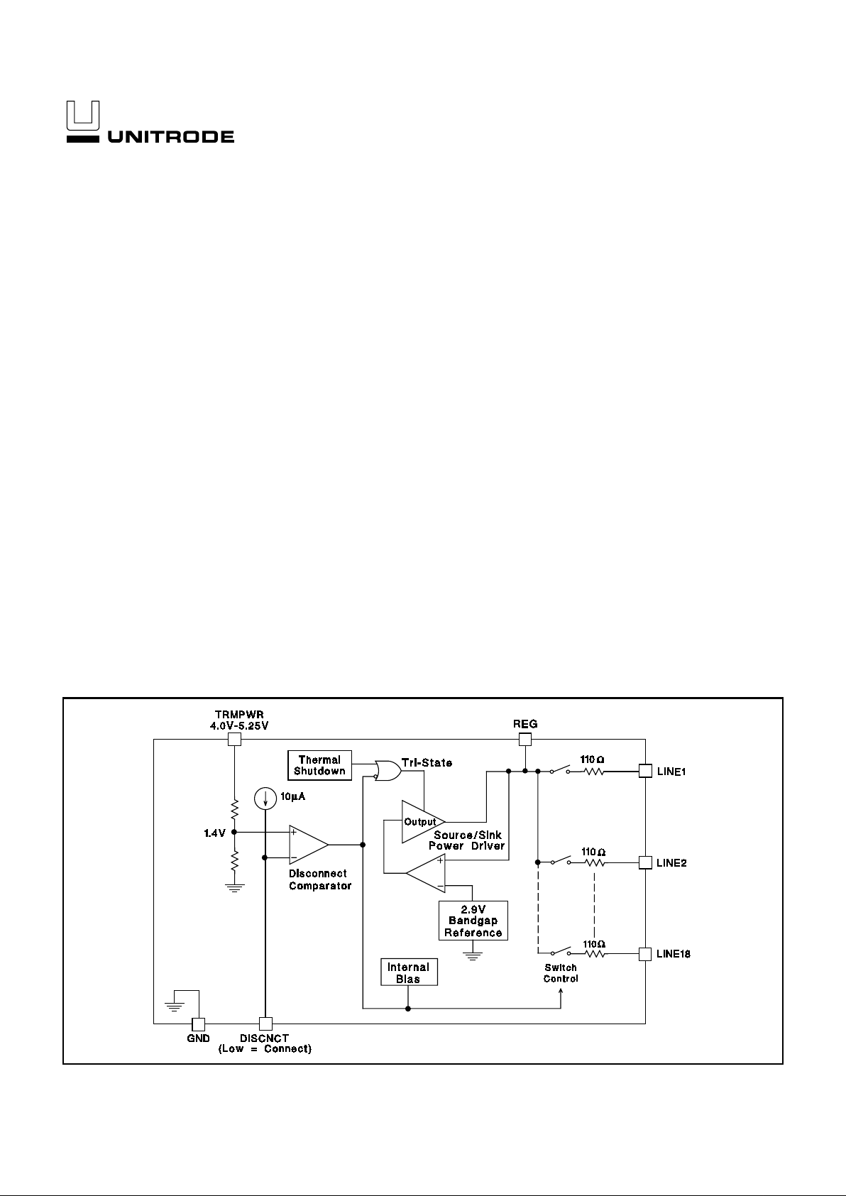
The UC5608 provi des 18 lines of active termination for a SCSI (Small
Computer Sy s t em s I nt er f ac e ) par all el bus. The SCS I s tandard recom-
mends active termination at both ends of the bus cable.
The UC5608 is pin-for-pin compatible with its predecessors, the
UC5601 and UC5602 - 18 Li ne Active Terminator. Parametrically the
UC5608 has a 5% tolerance on impedance and cu rren t compar ed to a
3% toleranc e on the UC56 01 and the sink current is increased from
20 to 200mA. The low side clamps have been removed. Custom
power packages are utilized to allow normal operation at full power
conditions (2 Watts).
When in disconnect mode the terminator will disconnect all terminat-
ing resistors and disable the regulator, greatly reducing standby
power. The output channels remain high impedance even without
Termpwr applied.
Internal circuit trimming is utilized to tri m the impedance to a 5% toler-
ance and, most importantly, to trim the outp ut current to a 5% toler-
ance, as c lose to the max SCSI spec as possible, which maximizes
noise margin in fast SCSI operation.
Other feat ures include 4.0 to 5.25V Termpwr, thermal shutdown and
current limit.
This device is offered in low the rmal re sistance v ersions of the indus-
try standard 28 pin wide body SOIC, 28 pin wide body TSSOP, and 28
pin PLCC, as well as 24 pin DIP.
UC5608
18-Line Low Capacitance SCSI Active Terminator
FEATURES DESCRIPTION
BLOCK DIAGRAM
Circuit Design Patented
3/97
UDG-94047
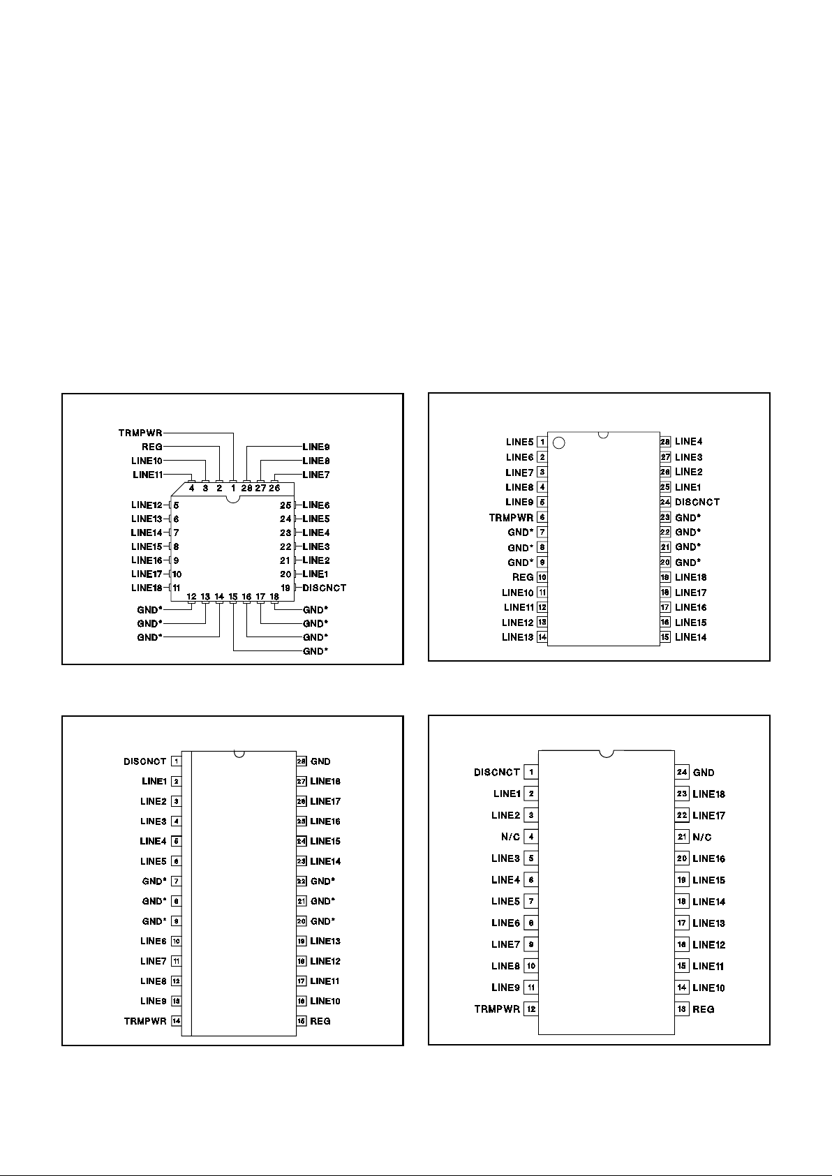
* PWP package pin 23 serves as signal ground; pins 7, 8, 9,
20, 21 and 22 serve as heats in k/ gro un d.
TSSOP-28 (To p View)
PWP Package
ABSOLUTE MAXIMUM RATINGS
Termpwr Vo ltage . . . . . . . . . . . . . . . . . . . . . . . . . . . . . . . . . . . . . . . . . . . . . . . . . . . +7V
Signal Line Voltage. . . . . . . . . . . . . . . . . . . . . . . . . . . . . . . . . . . . . . . . . . . . . 0V to +7V
Regulator Output Current . . . . . . . . . . . . . . . . . . . . . . . . . . . . . . . . . . . . . . . . . . . . . . 1A
Storage Temperature . . . . . . . . . . . . . . . . . . . . . . . . . . . . . . . . . . . . . −65°C to +150°C
Operating Temperature . . . . . . . . . . . . . . . . . . . . . . . . . . . . . . . . . . . −55°C to +150°C
Lead Temperature (Soldering, 10 Sec.) . . . . . . . . . . . . . . . . . . . . . . . . . . . . . . . +300°C
RECOMMENDED OPERATING CONDITIONS
Termpwr Voltage . . . . . . . . . . . . . . . . . . . . . . . . . . . . . . . . . . . . . . . . . . . 3.8V to 5.25V
Signal Line Voltage. . . . . . . . . . . . . . . . . . . . . . . . . . . . . . . . . . . . . . . . . . . . . 0V to +5V
Disconnect Input Voltage . . . . . . . . . . . . . . . . . . . . . . . . . . . . . . . . . . . . 0V to Termpwr
Unless otherwise specified all voltages are with respect to Ground. Currents are posi-
tive into, negative out of the specified terminal.
Consult Packaging Section of Unitrode Integrated Circuits databook for thermal limita-
tions and consid era ti on s of pac ka ges.
CONNECTION DIAGRAMS
PLCC-28 (Top View)
QP Package
* QP package pins 12 - 18 serve as both heatsink and signal
ground.
* DWP package pin 28 serves as signal ground; pins 7, 8, 9,
20, 21, 22 serve as heatsink/ground.
SOIC-28 (Top View)
DWP Package
Note: Drawings are not to scale.
DIL-24 (Top View)
N or J Package
UC5608
2
 Loading...