


UCC25705 |
UCC25705, UCC25706, UCC35705, UCC35706 |
|
|
||
|
|
HIGH SPEED VOLTAGE MODE PULSE WIDTH MODULATOR |
|
|
SLUS473A – NOVEMBER 1999 – REVISED MARCH 2001 |
|
|
|
|
D Greater Than 4-MHz Operation |
D, OR P PACKAGE |
|
|
(TOP VIEW) |
DIntegrated Oscillator / Voltage Feed Forward
Compensation |
|
ILIM |
|
|
1 |
8 |
|
VDD |
|
|
|
|
|||||
D >4:1 Input Voltage Range |
|
|
|
|||||
DGK PACKAGE |
FB |
|
|
2 |
7 |
|
OUT |
|
D 25-ns Current Limit Delay |
VFF |
|
|
3 |
6 |
|
GND |
|
(TOP VIEW) |
|
|
||||||
D Programmable Maximum Duty Cycle Clamp |
|
DISCH |
|
|
4 |
5 |
|
RC |
|
|
|
|
|
|
|
|
|
D |
Optocoupler Interface |
|
|
|
|
|
|
|
|
|
1 |
|
ILIM |
VDD |
|
8 |
|
||
|
50- A Start-Up Current |
|
|
|
|
||||
D |
|
|
|
|
|
|
|
|
|
D 4.2-mA Operating Current @ 1 MHz |
|
2 |
|
FB |
OUT |
|
7 |
|
|
|
|
|
VFF |
GND |
|
|
|
||
D Smallest Footprint of the 8-pin MSOP |
|
3 |
|
|
6 |
|
|||
|
|
|
|
|
|
|
|
||
|
Package Minimizes Board Area and Height |
|
|
|
RC |
|
|
|
|
|
|
4 |
|
DISCH |
|
5 |
|
||
description
The UCC35705 and UCC35706 devices are 8-pin voltage mode primary side controllers with fast over-current protection. These devices are used as core high-speed building blocks in high performance isolated and non-isolated power converters.
UCC35705/UCC35706 devices feature a high speed oscillator with integrated feed-forward compensation for improved converter performance. A typical current sense to output delay time of 25 ns provides fast response to overload conditions. The IC also provides an accurate programmable maximum duty cycle clamp for increased protection which can also be disabled for the oscillator to run at maximum possible duty cycle.
Two UVLO options are offered. The UCC35705 with lower turn-on voltage is intended for dc-to-dc converters while the higher turn-on voltage and the wider UVLO range of the UCC35706 is better suited for offline applications.
The UCC35705/UCC35706 family is offered in 8-pin MSOP (DGK), SOIC (D) and PDIP (P) packages.
typical application schematic
+ |
|
|
+ |
|
|
|
|
VOUT |
|
VIN |
|
|
– |
|
– |
|
|
|
|
4 |
VDD |
8 |
|
|
DISCH |
|
|
||
|
FB |
2 |
|
|
|
|
|
TPS2829 |
|
5 |
RC |
7 |
|
|
|
OUT |
|
||
3 |
VFF |
|
FET DRIVER |
|
|
|
|
||
|
|
|
SOFT |
|
6 |
GND ILIM |
1 |
START |
|
CIRCUIT |
||||
|
|
|
||
|
UCC35705/6 |
|
|
MODE = 1
UDG-99181
Please be aware that an important notice concerning availability, standard warranty, and use in critical applications of Texas Instruments semiconductor products and disclaimers thereto appears at the end of this data sheet.
|
|
|
PRODUCTION DATA information is current as of publication date. |
Copyright 2001, Texas Instruments Incorporated |
|
Products conform to specifications per the terms of Texas Instruments |
|
|
standard warranty. Production processing does not necessarily include |
|
|
testing of all parameters. |
|
|
www.ti.com |
1 |

UCC25705, UCC25706, UCC35705, UCC35706 |
|
HIGH SPEED VOLTAGE MODE PULSE WIDTH MODULATOR |
|
SLUS473A – NOVEMBER 1999 – REVISED MARCH 2001
absolute maximum ratings over operating free-air temperature (unless otherwise noted)†
Supply voltage . . . . . . . . . . . . . . . . . . . . . . . . . . . . . . . . . . . . . . . . . . . . . . . . . . . . . . . . . . . . . . . . . . . . . . . . . . . . . 15 V Input voltage (VFF,RC,ILIM) . . . . . . . . . . . . . . . . . . . . . . . . . . . . . . . . . . . . . . . . . . . . . . . . . . . . . . . . . . . . . . . . . . 7 V Input voltage (FB) . . . . . . . . . . . . . . . . . . . . . . . . . . . . . . . . . . . . . . . . . . . . . . . . . . . . . . . . . . . . . . . . . . . . . . . . . . 15 V Input current (DISCH) . . . . . . . . . . . . . . . . . . . . . . . . . . . . . . . . . . . . . . . . . . . . . . . . . . . . . . . . . . . . . . . . . . . . . . . 1 mA Output current (OUT) dc . . . . . . . . . . . . . . . . . . . . . . . . . . . . . . . . . . . . . . . . . . . . . . . . . . . . . . . . . . . . . . . . . ± 20 mA
Storage temperature, Tstg . . . . . . . . . . . . . . . . . . . . . . . . . . . . . . . . . . . . . . . . . . . . . . . . . . . . . . . . . –65° C to 150° C Junction temperature, TJ . . . . . . . . . . . . . . . . . . . . . . . . . . . . . . . . . . . . . . . . . . . . . . . . . . . . . . . . . . –55° C to 150° C Lead temperature (soldering, 10 sec.) . . . . . . . . . . . . . . . . . . . . . . . . . . . . . . . . . . . . . . . . . . . . . . . . . . . . . . . . 300° C
†Stresses beyond those listed under “absolute maximum ratings” may cause permanent damage to the device. These are stress ratings only, and functional operation of the device at these or any other conditions beyond those indicated under “recommended operating conditions” is not implied. Exposure to absolute-maximum-rated conditions for extended periods may affect device reliability.
‡All voltages are with respect to GND. Currents are positive into, negative out of the specified terminal. Consult Packaging Section of the Power
Supply Control Data Book (TI Literature Number SLUD003) for thermal limitations and considerations of packages.
AVAILABLE OPTIONS
|
|
|
Packaged Devices |
|
||
|
|
|
|
|
|
|
TA = TJ |
|
|
SOIC-8 |
PDIP-8 |
MSOP-8 |
|
|
UVLO Option |
Small Outline |
||||
|
|
† |
Plastic Dip (P) |
|||
|
|
(DGK)† |
||||
|
|
|
Small Outline (D) |
|
||
–40° C to 85° C |
8.8V/8V |
UCC25705D |
UCC25705P |
UCC25705DGK |
||
|
|
|
|
|||
12V/8V |
UCC25706D |
UCC25706P |
UCC25706DGK |
|||
|
|
|||||
|
|
|
|
|
|
|
0° C to 70° |
C |
8.8V/8V |
UCC35705D |
UCC35705P |
UCC35705DGK |
|
|
|
|
|
|||
12V/8V |
UCC35706D |
UCC35706P |
UCC35706DGK |
|||
|
|
|||||
|
|
|
|
|
|
|
†D (SOIC–8) and DGK (MSOP–8) packages are available taped and reeled. Add R suffix to device type (e.g. UCC35705DR) to order quantities of 2500 devices per reel for SOIC-8 and 2000 devices per reel for the MSOP-8.
electrical characteristics, VDD = 11 V, VIN = 30 V, RT = 47 k, RDISCH = 400 k, RFF = 14 k, CT = 220 pF, |
||||||||
CVDD = 0.1 F, and no load on the outputs, 0° C ≤ TA ≤ 70° C for the UCC3570x and –40° |
C ≤ TA ≤ |
85° C |
||||||
for the UCC2570x, TA = TJ, (unless otherwise specified) |
|
|
|
|
|
|
||
UVLO section (UCCx5705) |
|
|
|
|
|
|
|
|
|
|
|
|
|
|
|
|
|
|
PARAMETER |
TEST CONDITIONS |
MIN |
TYP |
MAX |
|
UNITS |
|
|
|
|
|
|
|
|
|
|
|
Start threshold |
|
8.0 |
8.8 |
9.6 |
|
V |
|
|
|
|
|
|
|
|
|
|
|
Stop threshold |
|
7.4 |
8.2 |
9.0 |
|
V |
|
|
|
|
|
|
|
|
|
|
|
Hysteresis |
|
0.3 |
0.6 |
1.0 |
|
V |
|
UVLO section (UCCx5706) |
|
|
|
|
|
|
|
|
|
|
|
|
|
|
|
|
|
|
PARAMETER |
TEST CONDITIONS |
MIN |
TYP |
MAX |
|
UNITS |
|
|
|
|
|
|
|
|
|
|
|
Start threshold |
|
11.2 |
12.0 |
12.8 |
|
V |
|
|
|
|
|
|
|
|
|
|
|
Stop threshold |
|
7.2 |
8.0 |
8.8 |
|
V |
|
|
|
|
|
|
|
|
|
|
|
Hysteresis |
|
3.5 |
4.0 |
4.5 |
|
V |
|
|
|
|
|
|
|
|
|
|
supply current section |
|
|
|
|
|
|
|
|
|
|
|
|
|
|
|
|
|
|
PARAMETER |
TEST CONDITIONS |
MIN |
TYP |
MAX |
|
UNITS |
|
|
|
|
|
|
|
|
|
|
|
Start-up current |
VDD = UVLO start – 1 V, VDD comparator off |
|
30 |
90 |
|
A |
|
|
IDD active |
VDD comparator on, oscillator running at 1 MHz |
|
4.2 |
5.0 |
|
mA |
|
|
|
|
|
|
|
|
|
|
2 |
www.ti.com |

|
UCC25705, UCC25706, UCC35705, UCC35706 |
|
HIGH SPEED VOLTAGE MODE PULSE WIDTH MODULATOR |
|
SLUS473A – NOVEMBER 1999 – REVISED MARCH 2001 |
|
|
electrical characteristics, VDD = 11 V, VIN = 30 V, RT = 47 k, RDISCH = 400 k, RFF = 14 k, CT = 220 pF, |
|||||||
CVDD = 0.1 F, and no load on the outputs, 0° |
C ≤ TA ≤ 70° C for the UCC3570x and –40° |
C ≤ TA ≤ |
85° C |
||||
for the UCC2570x, TA = TJ, (unless otherwise specified) |
|
|
|
|
|
||
line sense section |
|
|
|
|
|
|
|
|
|
|
|
|
|
|
|
PARAMETER |
|
TEST CONDITIONS |
MIN |
TYP |
MAX |
|
UNITS |
|
|
|
|
|
|
|
|
Low line comparator threshold |
|
|
0.95 |
1.00 |
1.05 |
|
V |
|
|
|
|
|
|
|
|
Input bias current (VFF) |
|
|
–100 |
|
100 |
|
nA |
oscillator section |
|
|
|
|
|
|
|
|
|
|
|
|
|
|
|
PARAMETER |
|
TEST CONDITIONS |
MIN |
TYP |
MAX |
|
UNITS |
|
|
|
|
|
|
|
|
Frequency |
VFF = 1.2 V to 4.8 V |
0.9 |
1.0 |
1.1 |
|
MHz |
|
|
|
|
|
|
|
|
|
CT peak voltage |
VFF = 1.2 V, |
See Note 1 |
|
1.2 |
|
|
V |
|
|
|
|
|
|
|
|
VFF = 4.8 V, |
See Note 1 |
|
4.8 |
|
|
V |
|
|
|
|
|
||||
|
|
|
|
|
|
|
|
CT valley voltage |
See Note 1 |
|
|
0 |
|
|
V |
|
|
|
|
|
|
|
|
NOTE 1: Ensured by design. Not production tested. |
|
|
|
|
|
|
|
current limit section |
|
|
|
|
|
|
|
|
|
|
|
|
|
|
|
PARAMETER |
|
TEST CONDITIONS |
MIN |
TYP |
MAX |
|
UNITS |
|
|
|
|
|
|
|
|
Input bias current |
|
|
0.2 |
–0.2 |
–1 |
|
µ A |
Current limit threshold |
|
|
180 |
200 |
220 |
|
mV |
|
|
|
|
|
|
|
|
Propagation delay, ILIM to OUT |
50 mV overdrive |
|
|
25 |
35 |
|
ns |
|
|
|
|
|
|
|
|
pulse width modulator section |
|
|
|
|
|
|
|
|
|
|
|
|
|
|
|
PARAMETER |
|
TEST CONDITIONS |
MIN |
TYP |
MAX |
|
UNITS |
|
|
|
|
|
|
|
|
FB input impedance |
VFB = 3 V |
|
30 |
50 |
90 |
|
kΩ |
Minimum duty cycle |
VFB < 2 V |
|
|
|
0 |
|
% |
Maximum duty cycle |
VFB = VDD, |
FOSC = 1 MHz |
70 |
75 |
80 |
|
% |
VDISCH = 0 V, |
FOSC = 1 MHz |
|
93 |
|
|
% |
|
|
|
|
|
||||
PWM gain |
VFF = 2.5 V, |
MODE = 1 |
|
12 |
|
|
%/V |
|
|
|
|
|
|
|
|
Propagation delay, PWM to OUT |
|
|
|
65 |
120 |
|
ns |
|
|
|
|
|
|
|
|
output section |
|
|
|
|
|
|
|
|
|
|
|
|
|
|
|
PARAMETER |
|
TEST CONDITIONS |
MIN |
TYP |
MAX |
|
UNITS |
|
|
|
|
|
|
|
|
VOH |
IOUT = –5 mA, |
VDD – output |
|
0.3 |
0.6 |
|
V |
VOL |
IOUT = 5 mA |
|
|
0.15 |
0.4 |
|
V |
Rise time |
CLOAD = 50 pF |
|
|
10 |
25 |
|
ns |
Fall time |
CLOAD = 50 pF |
|
|
10 |
25 |
|
ns |
www.ti.com |
3 |

UCC25705, UCC25706, UCC35705, UCC35706 |
|
HIGH SPEED VOLTAGE MODE PULSE WIDTH MODULATOR |
|
SLUS473A – NOVEMBER 1999 – REVISED MARCH 2001
pin descriptions
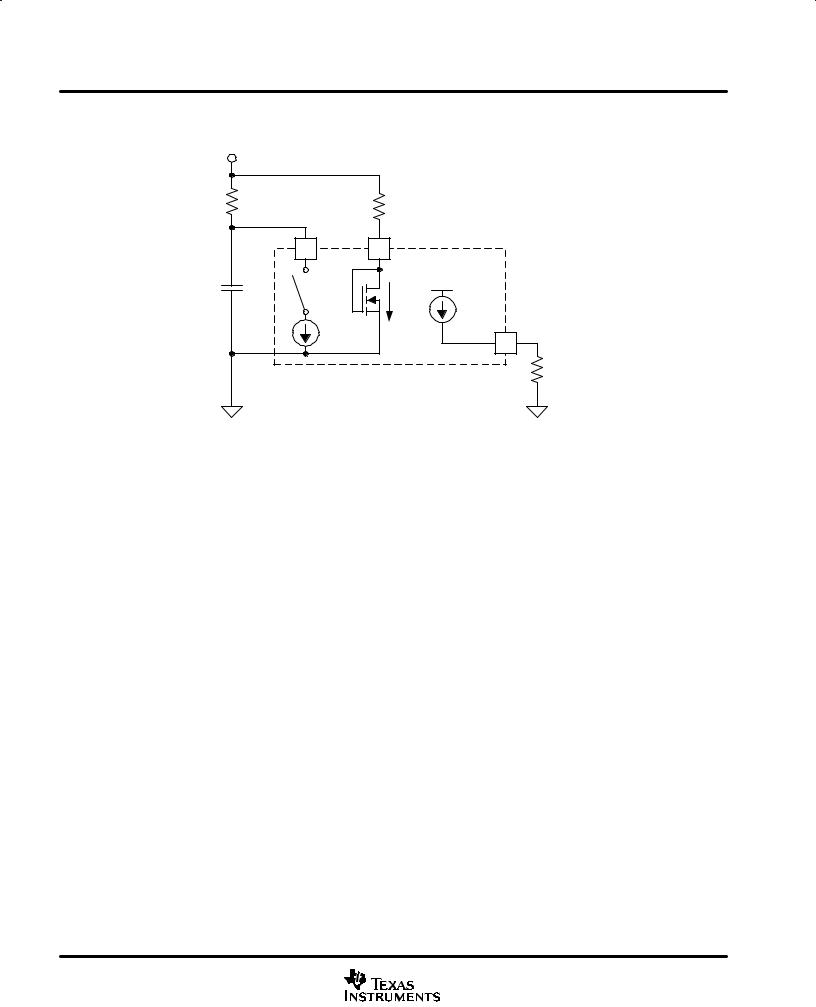
DISCH: A resistor to VIN sets the oscillator discharge current programming a maximum duty cycle. When grounded, an internal comparator switches the oscillator to a quick discharge mode. A small 100-pF capacitor between DISCH and GND may reduce oscillator jitter without impacting feed-forward performance. IDISCH must be between 25 µ A and 250 µ A over the entire VIN range.
FB: Input to the PWM comparator. This pin is intended to interface with an optocoupler. Input impedance is 50-kΩ typical.
GND: Ground return pin.
ILIM: Provides a pulse-by-pulse current limit by terminating the PWM pulse when the input is above 200 mV. This provides a high speed (25 ns typical) path to reset the PWM latch, allowing for a pulse-by-pulse current limit.
OUT: The output is intended to drive an external FET driver or other high impedance circuits, but is not intended to directly drive a power MOSFET. This improves the controller’s noise immunity. The output resistance of the PWM controller, typically 60 Ω pull-up and 30 Ω pull-down, will result in excessive rise and fall times if a power MOSFET is directly driven at the speeds for which the UCC35705/6 is optimized.
RC: The oscillator can be configured to provide a maximum duty cycle clamp. In this mode the on–time is set by RT and CT, while the off-time is set by RDISCH and CT. Since the voltage ramp on CT is proportional to VIN, feed-forward action is obtained. Since the peak oscillator voltage is also proportional to VIN, constant frequency operation is maintained over the full power supply input range. When the DISCH pin is grounded, the duty cycle clamp is disabled. The RC pin then provides a low impedance path to ground CT during the off time.
VDD: Power supply pin. This pin should be bypassed with a 0.1-µ F capacitor for proper operation. The undervoltage lockout function of the UCC35705/6 allows for a low current startup mode and ensures that all circuits become active in a known state. The UVLO thresholds on the UCC35705 are appropriate for a dc-to-dc converter application. The wider UVLO hysteresis of the UCC35706 (typically 4 V) is optimized for a bootstrap startup mode from a high impedance source.
VFF: The feed-forward pin provides the controller with a voltage proportional to the power supply input voltage. When
the oscillator is providing a duty cycle clamp, a current of 2 × IDISCH is sourced from the VFF pin. A single resistor RFF between VFF and GND then set VFF to:
VFF [ VIN 2 RFF
2 RFF ) RDISCH
When the DISCH pin is grounded and the duty cycle clamp is not used, the internal current source is disabled and a resistor divider from VIN is used to set VFF. In either case, when the voltage on VFF is less than 1.0 V, both the output and oscillator are disabled.
4 |
www.ti.com |

|
UCC25705, UCC25706, UCC35705, UCC35706 |
|
HIGH SPEED VOLTAGE MODE PULSE WIDTH MODULATOR |
|
SLUS473A – NOVEMBER 1999 – REVISED MARCH 2001 |
|
|
pin descriptions (continued) |
|
|
50 mV |
MODE |
|
|
|
|
|
|
|
|
|
|
|
– |
|
|
|
|
|
|
|
|
|
|
|
DISCH |
4 |
+ |
VDD |
1.0 V |
|
CLK |
|
|
|
|
|
|
|
|
|
|
LOW LINE |
|
|
|
|
|
|||
|
I |
|
2 * I (MODE=1) |
S |
Q |
PWM |
|
|
|
|||
|
|
– |
|
|
|
LATCH |
|
|
|
|||
|
|
|
|
|
|
|
|
|
||||
|
|
|
0 (MODE = 0) |
|
|
|
|
|
|
|||
|
|
|
|
RD |
|
|
|
|
|
|||
|
|
|
|
|
|
|
|
|
|
|||
|
|
|
|
|
+ |
|
|
|
|
|
|
|
|
|
|
|
|
|
RD |
Q |
|
|
7 |
OUT |
|
VFF |
3 |
|
|
|
|
|
RD |
|
|
|||
|
|
– |
|
|
|
|
|
|
|
|
||
|
|
|
|
|
|
|
|
|
|
|
|
|
RC |
5 |
|
|
+ |
S |
Q |
|
|
|
|
8 |
VDD |
|
|
|
|
|
|
|
|
|
|
|
||
|
|
30 * I (MODE=1) |
+ |
RD Q |
|
|
UVLO |
|
|
|
||
|
|
– |
|
|
|
|
|
|
|
|||
|
|
|
|
|
|
UCC35705 (8.8 V/8 V) |
|
|
||||
|
|
80 Ω |
(MODE = 0) |
|
|
|
|
|
|
|||
|
|
|
|
|
|
|
|
|
||||
|
|
|
|
|
|
|
|
|
UCC35706 (12 V/8 V) |
|
|
|
|
|
|
100 mV |
|
|
|
|
|
|
|
|
|
|
|
|
|
0.7 V |
|
|
|
|
|
|
6 |
GND |
|
|
|
|
|
PWM |
|
|
|
|
|
|
|
|
|
|
|
|
|
|
|
|
|
|
|
|
|
|
|
|
+ |
|
– |
|
|
|
|
|
|
FB |
2 |
|
|
|
|
|
|
|
200 mV |
|
|
|
|
|
|
|
+ |
|
CURRENT LIMIT |
|
|
||||
|
|
|
30 kΩ |
|
|
|
|
|
|
|
||
|
|
|
20 kΩ |
1 pF |
|
|
+ |
|
|
|
||
|
|
|
|
|
|
|
|
|
||||
|
|
|
|
|
|
|
|
|
– |
|
1 |
ILIM |
Figure 1. Block Diagram
FUNCTIONAL DESCRIPTION
oscillator and PWM
The oscillator can be programmed to provide a duty cycle clamp or be configured to run at the maximum possible duty cycle.
The PWM latch is set during the oscillator discharge and is reset by the PWM comparator when the CT waveform is greater than the feedback voltage. The voltage at the FB pin is attenuated before it is applied to the PWM comparator. The oscillator ramp is shifted by approximately 0.65-V at room temperature at the PWM comparator. The offset has a temperature coefficient of approximately –2 mV/° C.
The ILIM comparator adds a pulse by pulse current limit by resetting the PWM latch when VILIM > 200 mV. The PWM latch is also reset by a low line condition (VFF <1.0 V).
All reset conditions are dominant; asserting any output will force a zero duty cycle output.
oscillator with duty cycle clamp (MODE = 1)
The timing capacitor CT is charged from ground to VFF through RT. The discharge path is through an on-chip current
sink that has a value of 30 × IDISCH, where IDISCH is the current through the external resistor RDISCH. Since the charge and discharge currents are both proportional to VIN, their ratio, and the maximum duty cycle remains constant
as VIN varies.
www.ti.com |
5 |
UCC25705, UCC25706, UCC35705, UCC35706 |
|
HIGH SPEED VOLTAGE MODE PULSE WIDTH MODULATOR |
|
SLUS473A – NOVEMBER 1999 – REVISED MARCH 2001
FUNCTIONAL DESCRIPTION
V IN
R T |
|
R DISCH |
|
|
RC |
DISCH |
|
5 |
4 |
|
|
|
|
|
VDD |
C T |
|
IDISCH |
2 * IDISCH |
|
|
|
|
|
30 * I DISCH |
|
VFF |
3
R FF
Figure 2. Duty Cycle Clamp (MODE = 1)
The on-time is approximately:
TON +T |
RT |
CT |
where T+ |
VFF |
2 RFF |
|||||||||||||
|
|
|
[ |
|
|
|
||||||||||||
V |
IN |
R |
DISCH |
|||||||||||||||
|
|
|
|
|
|
|
|
|
|
|
|
|
|
|
|
|||
The off-time is: |
|
|
|
|
|
|
|
|
|
|
|
|
|
|
|
|
|
|
TOFF +T |
|
CT |
RT |
|
RDISCH |
|
|
|
|
|
|
|||||||
30 |
RT * RDISCH |
|
|
|
|
|
||||||||||||
|
|
|
|
|
|
|
||||||||||||
The frequency is: |
|
|
|
|
|
|
|
|
|
|
|
|
|
|
|
|
|
|
f + |
|
1 |
|
|
|
|
|
1 |
|
|
|
|
|
|||||
T |
RT |
CT |
1 ) |
|
RDISCH |
|
|
|||||||||||
|
|
|
|
|
|
|
30 RT*RDISCH |
|||||||||||
|
|
|
|
|
|
|
|
|
|
|||||||||
The maximum duty cycle is: |
|
|
|
|
|
|
|
|
|
|
|
|
||||||
|
|
|
|
|
TON |
|
|
|
|
|
|
RDISCH |
|
|
||||
Duty Cycle + |
|
+ 1 * |
|
|
|
|||||||||||||
TON ) TOFF |
30 |
RT |
||||||||||||||||
6 |
www.ti.com |
 Loading...