


 Loading...
UCC27323, UCC27324, UCC27325
UCC37323, UCC37324, UCC37325
SLUS492B – JUNE 2001 – REVISED SEPTEMBER 2002
DUAL 4 A PEAK HIGH SPEED LOW-SIDE POWER MOSFET DRIVERS
FEATURES
DIndustry-Standard Pin-Out
DHigh Current Drive Capability of ± 4 A at the
Miller Plateau Region
DEfficient Constant Current Sourcing Using a Unique BiPolar & CMOS Output Stage
DTTL/CMOS Compatible Inputs Independent of Supply Voltage
D20-ns Typical Rise and 15-ns Typical Fall Times with 1.8-nF Load
DTypical Propagation Delay Times of 25 ns with Input Falling and 35 ns with Input Rising
D4-V to 15-V Supply Voltage
DSupply Current of 0.3 mA
DDual Outputs Can Be Paralleled for Higher Drive Current
DAvailable in Thermally Enhanced MSOP PowerPADTM Package with 4.7° C/W θ jc
DRated From –40° C to 85° C
APPLICATIONS
DSwitch Mode Power Supplies
DDC/DC Converters
DMotor Controllers
DLine Drivers
DESCRIPTION
The UCC37323/4/5 family of high-speed dual MOSFET drivers can deliver large peak currents into capacitive loads.Three standard logic options are offered – dual-inverting, dual-noninverting and one-inverting and one-noninverting driver. The thermally enhanced 8-pin PowerPADTM MSOP package (DGN) drastically lowers the thermal resistance to improve long-term reliability. It is also offered in the standard SOIC-8 (D) or PDIP-8
(P) packages.
Using a design that inherently minimizes shoot-through current, these drivers deliver 4-A of current where it is needed most at the Miller plateau region during the MOSFET switching transition. A unique BiPolar and MOSFET hybrid output stage in parallel also allows efficient current sourcing and sinking at low supply voltages.
BLOCK DIAGRAM
N/C 1 |
INVERTING |
8 |
N/C |
|
|||
INA 2 |
NON–INVERTING |
7 |
OUTA |
|
|
||
|
|
|
|
GND 3 |
INVERTING |
|
|
|
6 |
VDD |
|
INB 4 |
NON–INVERTING |
5 |
OUTB |
|
|
||
|
|
|
UDG–01063
PowerPADt is a trademark of Texas Instruments Incorporated.
Please be aware that an important notice concerning availability, standard warranty, and use in critical applications of Texas Instruments semiconductor products and disclaimers thereto appears at the end of this data sheet.
|
|
|
PRODUCTION DATA information is current as of publication date. |
Copyright 2002, Texas Instruments Incorporated |
|
Products conform to specifications per the terms of Texas Instruments |
|
|
standard warranty. Production processing does not necessarily include |
|
|
testing of all parameters. |
|
|
www.ti.com |
1 |

UCC27323, UCC27324, UCC27325
UCC37323, UCC37324, UCC37325
SLUS492B – JUNE 2001 – REVISED SEPTEMBER 2002
ORDERING INFORMATION
OUTPUT |
TEMPERATURE RANGE |
|
PACKAGED DEVICES |
|
|
|
|
|
|
||
|
MSOP-8 PowerPAD |
|
|
||
CONFIGURATION |
TA = TJ |
SOIC-8 (D) |
|
PDIP-8 (P) |
|
(DGN)} |
|
||||
|
|
|
|
|
|
|
|
|
|
|
|
Dual inverting |
–40° C to +85° C |
UCC27323D |
UCC27323DGN |
|
UCC27323P |
|
|
|
|
|
|
0° C to +70° C |
UCC37323D |
UCC37323DGN |
|
UCC37323P |
|
|
|
||||
|
|
|
|
|
|
Dual nonInverting |
–40° C to +85° C |
UCC27324D |
UCC27324DGN |
|
UCC27324P |
|
|
|
|
|
|
0° C to +70° C |
UCC37324D |
UCC37324DGN |
|
UCC37324P |
|
|
|
||||
|
|
|
|
|
|
One inverting, |
–40° C to +85° C |
UCC27325D |
UCC27325DGN |
|
UCC27325P |
|
|
|
|
|
|
one noninverting |
0° C to +70° C |
UCC37325D |
UCC37325DGN |
|
UCC37325P |
† D (SOIC–8) and DGN (PowerPAD–MSOP) packages are available taped and reeled. Add R suffix to device type (e.g. UCC27323DR, UCC27324DGNR) to order quantities of 2,500 devices per reel for D or 1,000 devices per reel for DGN package.
‡ The PowerPAD is not directly connected to any leads of the package. However, it is electrically and thermally connected to the substrate which is the ground of the device.
D, DGN, OR P PACKAGE
(TOP VIEW)
N/A |
1 |
8 |
N/A |
INA |
2 |
7 |
OUTA |
GND |
3 |
6 |
VDD |
INB |
4 |
5 |
OUTB |
(DUAL INVERTING)
D, DGN, OR P PACKAGE |
D, DGN, OR P PACKAGE |
||||||||||||
|
|
(TOP VIEW) |
|
|
|
(TOP VIEW) |
|
||||||
N/A |
|
|
|
|
|
N/A |
N/A |
|
|
|
|
N/A |
|
|
|
|
|
|
|
|
|
|
|||||
1 |
|
|
|
8 |
1 |
|
8 |
|
|||||
|
|
|
|
|
|
OUTA |
|
|
|
|
|
|
OUTA |
|
|
|
|
|
|
|
|
|
|
|
|
||
INA |
2 |
|
|
|
7 |
INA |
2 |
|
|
7 |
|
||
|
|
|
|||||||||||
|
|
|
|
|
|
|
|
|
|
|
|
|
|
|
|
|
|
|
|
|
|
|
|
|
|
|
|
GND |
3 |
|
|
|
6 |
VDD |
GND |
3 |
|
6 |
|
VDD |
|
|
|
|
|
|
|
OUTB |
|
|
|
|
|
OUTB |
|
|
|
|
|
|
|
|
|
|
|
|
|||
INB |
4 |
|
|
|
5 |
INB |
4 |
|
5 |
|
|||
|
|
|
|||||||||||
|
|
|
|
|
|
|
|
|
|
|
|
|
|
|
|
|
|
|
|
|
|
|
|
|
|
|
|
(DUAL NONINVERTING) |
(ONE INVERTING, |
|
|||||||||||
ONE NONINVERTING) |
|
||||||||||||
power dissipation rating table
|
|
|
|
|
|
Power Rating (mW) |
Derating Factor Above |
|
PACKAGE |
SUFFIX |
Θ jc (° C/W) |
Θ ja (° C/W) |
|
70° C (mW/ C) See |
|
|
|
TA = 70° C See Note 1 |
|||||
|
|
|
|
|
|
Note 1 |
|
|
|
|
|
|
|
|
|
|
|
|
|
|
|
|
|
|
SOIC-8 |
D |
42 |
84 – 160} |
|
344–655 See Note 2 |
6.25 – 11.9 See Note 2 |
|
|
|
|
|
|
|
|
|
PDIP-8 |
P |
49 |
110 |
|
500 |
9 |
|
|
|
|
|
|
|
|
|
MSOP PowerPAD-8 |
DGN |
4.7 |
50 – 59} |
|
1370 |
17.1 |
|
See Note 3 |
|
|||||
|
|
|
|
|
|
|
|
|
|
|
|
|
|
|
|
Notes: 1. 125° C operating junction temperature is used for power rating calculations |
|
|
|||||
2.The range of values indicates the effect of pc–board. These values are intended to give the system designer an indication of the best and worst case conditions. In general, the system designer should attempt to use larger traces on the pc–board where possible in order to spread the heat away form the device more effectively. For information on the PowerPADt package, refer to Technical Brief, PowerPad Thermally Enhanced Package, Texas Instrument s Literature No. SLMA002 and Application Brief, PowerPad Made Easy, Texas Instruments Literature No. SLMA004.
3.The PowerPAD is not directly connected to any leads of the package. However, it is electrically and thermally connected to the substrate which is the ground of the device.
Table 1. Input/Output Table
|
INPUTS (VIN_L, VIN_H) |
UCC37323 |
UCC37324 |
UCC37325 |
|
||||
|
|
|
|
|
|
|
|
|
|
|
INA |
INB |
OUTA |
OUTB |
OUTA |
OUTB |
OUTA |
OUTB |
|
|
|
|
|
|
|
|
|
|
|
|
L |
L |
H |
H |
L |
L |
H |
L |
|
|
|
|
|
|
|
|
|
|
|
|
L |
H |
H |
L |
L |
H |
H |
H |
|
|
|
|
|
|
|
|
|
|
|
|
H |
L |
L |
H |
H |
L |
L |
L |
|
|
|
|
|
|
|
|
|
|
|
|
H |
H |
L |
L |
H |
H |
L |
H |
|
|
|
|
|
|
|
|
|
|
|
2 |
www.ti.com |

UCC27323, UCC27324, UCC27325
UCC37323, UCC37324, UCC37325
SLUS492B – JUNE 2001 – REVISED SEPTEMBER 2002
absolute maximum ratings over operating free-air temperature (unless otherwise noted)†
Supply voltage, VDD . . . . . . . . . . . . . . . . . . . . . . . . . . . . . . . . . . . . . . . . . . . . . . . . . . . . . . . . . . . . . . . . –0.3 V to 16 V Output current (OUTA, OUTB) DC, IOUT_DC . . . . . . . . . . . . . . . . . . . . . . . . . . . . . . . . . . . . . . . . . . . . . . . . . . 0.3 A
Pulsed, (0.5 s), IOUT_PULSED . . . . . . . . . . . . . . . . . . . . . . . . . . . . . . . . . . 4.5 A . . .
Power dissipation at TA = 25° C (DGN package) . . . . . . . . . . . . . . . . . . . . . . . . . . . . . . . . . . . . . . . . . . . . . . . . . 3 W (D package) . . . . . . . . . . . . . . . . . . . . . . . . . . . . . . . . . . . . . . . . . . . . . . . . 650 mW
(P package) . . . . . . . . . . . . . . . . . . . . . . . . . . . . . . . . . . . . . . . . . . . . . . . . 350 mW
Junction operating temperature, TJ . . . . . . . . . . . . . . . . . . . . . . . . . . . . . . . . . . . . . . . . . . . . . . . . . –55° C to 150° C Storage temperature, Tstg . . . . . . . . . . . . . . . . . . . . . . . . . . . . . . . . . . . . . . . . . . . . . . . . . . . . . . . . . –65° C to 150° C Lead temperature (soldering, 10 sec.), . . . . . . . . . . . . . . . . . . . . . . . . . . . . . . . . . . . . . . . . . . . . . . . . . . . . . . . 300° C
†Stresses beyond those listed under “absolute maximum ratings” may cause permanent damage to the device. These are stress ratings only, and functional operation of the device at these or any other conditions beyond those indicated under “recommended operating conditions” is not implied. Exposure to absolute-maximum-rated conditions for extended periods may affect device reliability.
‡ All voltages are with respect to GND. Currents are positive into, negative out of the specified terminal.
electrical characteristics, VDD = 4.5 V to 15 V, TA = TJ, (unless otherwise noted)
input (INA, INB)
PARAMETER |
TEST CONDITION |
MIN |
TYP |
MAX |
UNITS |
|
|
|
|
|
|
VIN_H, logic 1 input threshold |
|
2 |
|
|
V |
|
|
|
|
|
|
VIN_L, logic 0 input threshold |
|
|
|
1 |
V |
|
|
|
|
|
|
Input current |
0 V <= VIN <= VDD |
–10 |
0 |
10 |
µ A |
output (OUTA, OUTB) |
|
|
|
|
|
PARAMETER |
|
TEST CONDITION |
|
MIN |
TYP |
MAX |
UNITS |
|
|
|
|
|
|
|
|
Output current |
VDD = 14 V, |
See Note 1, |
See Note 2 |
|
4 |
|
A |
VOH, high-level output voltage |
VOH = VDD – VOUT, |
|
IOUT = –10 mA |
|
300 |
450 |
mV |
VOL, low-level output level |
IOUT = 10 mA |
|
|
|
22 |
40 |
mV |
Output resistance high |
TA = 25° C, |
IOUT = –10 mA, |
VDD = 14 V, |
25 |
30 |
35 |
Ω |
|
See Note 3 |
|
|
|
|
|
|
|
TA = full range, |
IOUT = –10 mA, |
VDD = 14 V, |
18 |
|
42 |
Ω |
|
See Note 3 |
|
|
|
|
|
|
Output resistance low |
TA = 25° C, |
IOUT = 10 mA, |
VDD = 14 V, |
1.9 |
2.2 |
2.5 |
Ω |
|
See Note 3 |
|
|
|
|
|
|
|
|
|
|
|
|
|
|
|
TA = full range |
IOUT = 10 mA, |
VDD = 14 V, |
1.2 |
|
4.0 |
Ω |
|
See Note 3 |
|
|
|
|
|
|
Latch-up protection |
See Note 1 |
|
|
500 |
|
|
mA |
|
|
|
|
|
|
|
|
NOTES: 1. Ensured by design. Not tested in production.
2.The pullup / pulldown circuits of the driver are bipolar and MOSFET transistors in parallel. The pulsed output current rating is the combined current from the bipolar and MOSFET transistors.
3.The pullup / pulldown circuits of the driver are bipolar and MOSFET transistors in parallel. The output resistance is the RDS(ON) of the MOSFET transistor when the voltage on the driver output is less than the saturation voltage of the bipolar transistor.
www.ti.com |
3 |
UCC27323, UCC27324, UCC27325
UCC37323, UCC37324, UCC37325
SLUS492B – JUNE 2001 – REVISED SEPTEMBER 2002
electrical characteristics, VDD = 4.5 V to 15 V, TA = TJ, (unless otherwise noted)
switching time
PARAMETER |
TEST CONDITION |
MIN |
TYP |
MAX |
UNITS |
|
|
|
|
|
|
|
|
tR, rise time (OUTA, OUTB) |
CLOAD = 1.8 nF, |
See Figure 1 |
|
20 |
40 |
ns |
tF, fall time (OUTA, OUTB) |
CLOAD = 1.8 nF, |
See Figure 1 |
|
15 |
40 |
ns |
tD1, delay, IN rising (IN to OUT) |
CLOAD = 1.8 nF, |
See Figure 1 |
|
25 |
40 |
ns |
tD2, delay, IN falling (IN to OUT) |
CLOAD = 1.8 nF, |
See Figure 1 |
|
35 |
50 |
ns |
overall
PARAMETER |
|
TEST CONDITION |
MIN |
TYP |
MAX |
UNITS |
|
|
|
|
|
|
|
|
|
|
|
INA = 0 V, |
INB = 0 V |
|
300 |
450 |
|
|
|
|
|
|
|
|
|
|
UCCx7323 |
INA = 0 V, |
INB = HIGH |
|
300 |
450 |
|
|
|
|
|
|
|
|
|
|
INA = HIGH, |
INB = 0 V |
|
300 |
450 |
|
|
|
|
|
|
||||
|
|
|
|
|
|
|
|
|
|
INA = HIGH, |
INB = HIGH |
|
300 |
450 |
|
|
|
|
|
|
|
|
|
|
|
INA = 0 V, |
INB = 0 V |
|
2 |
50 |
|
|
|
|
|
|
|
|
|
IDD, static operating current |
UCCx7324 |
INA = 0 V, |
INB = HIGH |
|
300 |
450 |
A |
|
|
|
|
|
|||
INA = HIGH, |
INB = 0 V |
|
300 |
450 |
|||
|
|
|
|
||||
|
|
|
|
|
|
|
|
|
|
INA = HIGH, |
INB = HIGH |
|
600 |
750 |
|
|
|
|
|
|
|
|
|
|
|
INA = 0 V, |
INB = 0 V |
|
150 |
300 |
|
|
|
|
|
|
|
|
|
|
UCCx7325 |
INA = 0 V, |
INB = HIGH |
|
450 |
600 |
|
|
|
|
|
|
|
|
|
|
INA = HIGH, |
INB = 0 V |
|
150 |
300 |
|
|
|
|
|
|
||||
|
|
|
|
|
|
|
|
|
|
INA = HIGH, |
INB = HIGH |
|
450 |
600 |
|
NOTES: 1. Ensured by design. Not production.
2.The pullup / pulldown circuits of the driver are bipolar and MOSFET transistors in parallel. The peak output current rating is the combined current from the bipolar and MOSFET transistors.
3.The pullup / pulldown circuits of the driver are bipolar and MOSFET transistors in parallel. The output resistance is the RDS(ON) of the MOSFET transistor when the voltage on the driver output is less than the saturation voltage of the bipolar transistor.
(a) |
(b) |
||||
+5V |
|
|
|
||
|
|
90% |
|
|
90% |
|
|
||||
INPUT |
INPUT |
||||
10% |
|
|
|
|
|
10% |
|
0V |
|
|
|
|
|
|
|
t |
D1 |
t |
t |
D2 |
tf |
t |
F |
|
F |
|
|
tF |
|||
16V |
|
|
|
|
|
|
|
|
|
|
|
|
|
|
|
90% |
|
90% |
|
|
|
|
|
|
|
|
|
|
|
|
90% |
|
|
|
|
|
|
|
|||||
|
|
|
|
|
|
|
|
tD1 |
|
|
|
|
|
|
|
|
|
|
|
|
||||||||
|
|
|
|
|
|
|
|
|
|
|
|
|
|
|
|
|
|
|
|
|
|
|
|
|
|
|
|
|
OUTPUT |
|
|
|
|
|
|
|
|
|
|
|
|
|
|||||||||||||||
|
|
|
|
|
OUTPUT |
|
|
|
|
|
|
|
|
|
|
|
|
|
|
|
|
|
|
|
||||
|
|
|
|
|
|
|
|
|
|
|
|
|
|
|
|
|
|
|
|
|
|
|
|
|||||
|
|
|
|
|
|
|
|
|
|
|
|
|
|
|
|
|
|
|
|
|
|
|
||||||
|
|
|
|
|
|
|
|
|
|
|
|
|||||||||||||||||
|
|
|
|
|
|
|
|
|
|
|
|
|
|
|
|
|
|
tD2 |
|
|||||||||
|
|
|
|
|
|
|
|
|
|
|
|
|
|
|
|
|
|
|
||||||||||
|
|
|
|
|
|
|
|
|
|
|
|
|
|
|
|
|
|
|||||||||||
0V |
|
10% |
|
|
|
|
|
10% |
|
|||||||||||||||||||
|
|
|
|
|
|
|
|
|
|
|
|
|||||||||||||||||
|
|
|
|
|
|
|
|
|
|
|
|
|
|
|
|
|
|
|
|
|
|
|
|
|
|
|||
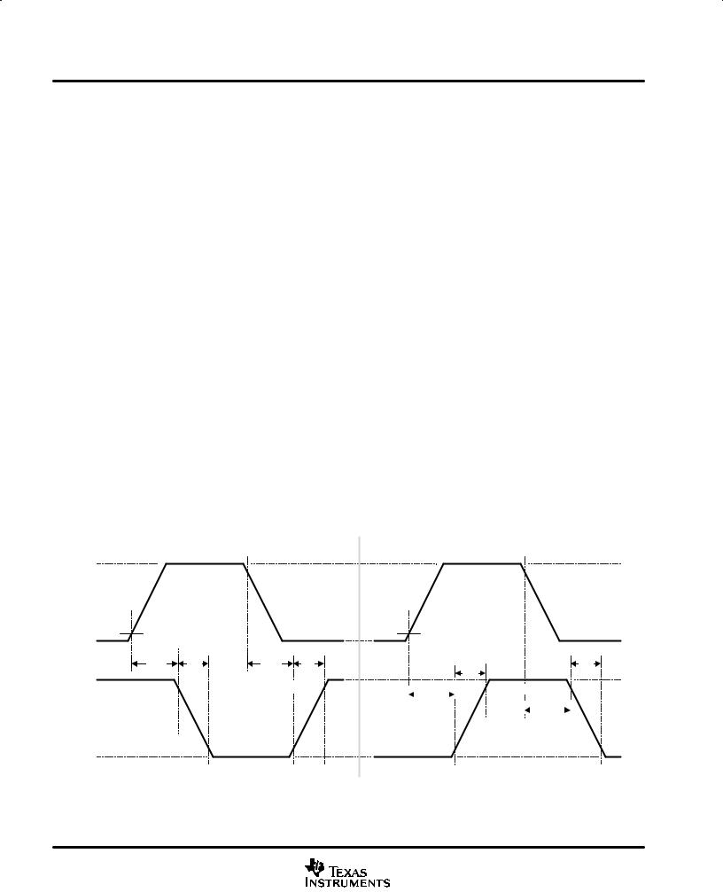
Figure 1. Switching Waveforms for (a) Inverting Driver and (b) Noninverting Driver
4 |
www.ti.com |

UCC27323, UCC27324, UCC27325
UCC37323, UCC37324, UCC37325
SLUS492B – JUNE 2001 – REVISED SEPTEMBER 2002
|
|
|
Terminal Functions |
|
|
|
|
|
|
|
TERMINAL |
|
FUNCTION |
|
|
|
|
||
NO. |
NAME |
I/O |
||
|
||||
|
|
|
|
|
1 |
N/C |
– |
No connection. Should be grounded. |
|
|
|
|
|
|
2 |
INA |
I |
Input A. Input signal of the A driver which has logic compatible threshold and hysteresis. |
|
|
|
|
If not used, this input should be tied to either VDD or GND. It should not be left floating. |
|
|
|
|
|
|
3 |
GND |
– |
Common ground. This ground should be connected very closely to the source of the |
|
|
|
|
power MOSFET which the driver is driving. |
|
|
|
|
|
|
4 |
INB |
I |
Input B. Input signal of the A driver which has logic compatible threshold and hysteresis. |
|
|
|
|
If not used, this input should be tied to either VDD or GND. It should not be left floating. |
|
|
|
|
|
|
5 |
OUTB |
O |
Driver output B. The output stage is capable of providing 4-A drive current to the gate of |
|
|
|
|
a power MOSFET. |
|
|
|
|
|
|
6 |
VDD |
I |
Supply. Supply voltage and the power input connection for this device. |
|
|
|
|
|
|
7 |
OUTA |
O |
Driver output A. The output stage is capable of providing 4-A drive current to the gate of |
|
|
|
|
a power MOSFET. |
|
|
|
|
|
|
8 |
N/C |
– |
No Connection. Should be grounded. |
|
|
|
|
|
APPLICATION INFORMATION
general information
High frequency power supplies often require high-speed, high-current drivers such as the UCC37323/4/5 family. A leading application is the need to provide a high power buffer stage between the PWM output of the control IC and the gates of the primary power MOSFET or IGBT switching devices. In other cases, the driver IC is utilized to drive the power device gates through a drive transformer. Synchronous rectification supplies also have the need to simultaneously drive multiple devices which can present an extremely large load to the control circuitry.
Driver ICs are utilized when it is not feasible to have the primary PWM regulator IC directly drive the switching devices for one or more reasons. The PWM IC may not have the brute drive capability required for the intended switching MOSFET, limiting the switching performance in the application. In other cases there may be a desire to minimize the effect of high frequency switching noise by placing the high current driver physically close to the load. Also, newer ICs that target the highest operating frequencies may not incorporate onboard gate drivers at all. Their PWM outputs are only intended to drive the high impedance input to a driver such as the UCC37323/4/5. Finally, the control IC may be under thermal stress due to power dissipation, and an external driver can help by moving the heat from the controller to an external package.
www.ti.com |
5 |
Loading...