


UCC383T-5
Texas Instruments UCC383T-5, UCC383T-3, UCC383TDTR-ADJ, UCC383TDTR-3, UCC383TD-ADJ Datasheet
...
SLUS215 - OCTOBER 1998
FEATURES
• Precision Positive Series Pass
Voltage Regulation
• 0.45V Dropout at 3A
• 50mV Dropout at 10mA
• Quiescent Current Under
650µA Irrespective of Load
• Adjustable (5 Lead) Output
Voltage Version
• Fixed (3 Lead) Versions for
3.3V and 5V Outputs
• Logic Shutdown Capability
• Short Circuit Power Limit of
3% •V
IN
• I
SHORT
• Low V
OUT
to V
IN
Reverse
Leakage
• Thermal Shutdown
DESCRIPTION
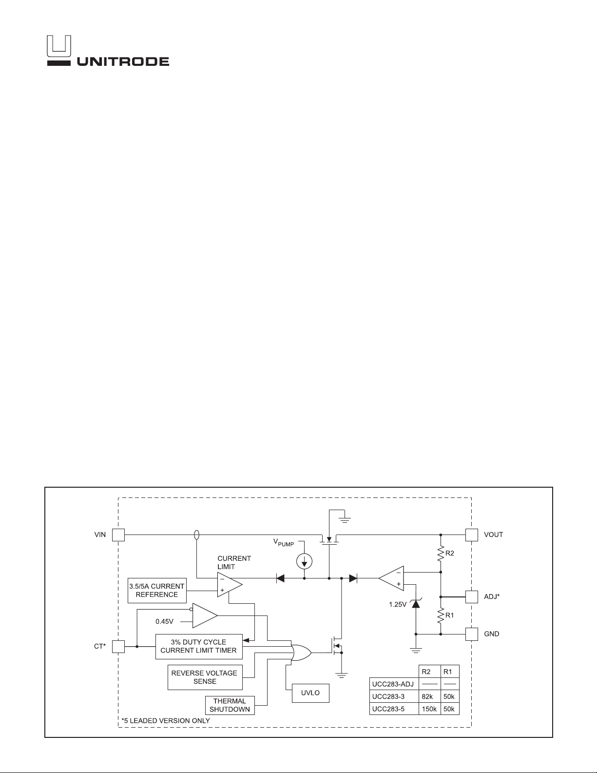
The UCC283-3/-5/-ADJ family of positive linear series pass regulators are tailored
for low drop out applications where low quiescent power is important. Fabricated
with a BiCMOS technology ideally suited for low input to output differential applica-
tions, the UCC283-5 will pass 3A while requiring only 0.45V of typical input voltage
headroom (guaranteed 0.6V dropout). These regulators include reverse voltage
sensing that prevents current in the reverse direction. Quiescent current is always
less than 650µA. These devices have been internally compensated in such a man-
ner that the need for a minimum output capacitor has been eliminated.
UCC283-3 and UCC283-5 versions are in 3 lead packages and have preset outputs
at 3.3V and 5.0V respectively. The output voltage is regulated to 1.5% at room tem-
perature. The UCC283-ADJ version, in a 5 lead package, regulates the output volt-
age programmed by an external resistor ratio.
Short circuit current is internally limited. The device responds to a sustained over-
current condition by turning off after a T
ON
delay. The device then stays off for a pe-
riod, T
OFF
, that is 32 times the T
ON
delay. The device then begins pulsing on and off
at the T
ON
/(T
ON
+T
OFF
) duty cycle of 3%. This drastically reduces the power dissipa-
tion during short circuit and means heat sinks need only accommodate normal op-
eration. On the 3 leaded versions of the device T
ON
is fixed at 750µs, on the
adjustable 5 leaded versions an external capacitor sets the on time — the off time
is always 32 times T
ON
. The external timing control pin, CT, on the five leaded ver-
sions also serves as a shutdown input when pulled low.
Internal power dissipation is further controlled with thermal overload protection cir-
cuitry. Thermal shutdown occurs if the junction temperature exceeds 165°C. The
chip will remain off until the temperature has dropped 20°C.
The UCC283 series is specified for operation over the industrial range of −40°Cto
+85°C, and the UCC383 series is specified from 0°C to +70°C. These devices are
available in 3 and 5 pin TO-220 and TO-263 power packages.
UCC283-3/-5/-ADJ
UCC383-3/-5/-ADJ
Low Dropout 3 Ampere Linear Regulator Family
BLOCK DIAGRAM
UDG-98133
2
UCC283-3/-5/-ADJ
UCC383-3/-5/-ADJ
ABSOLUTE MAXIMUM RATINGS
VIN .........................................................9V
CT.......................................−0.3 to 3V
ADJ......................................−0.3 to 9V
Storage Temperature ...................−65°C to +150°C
Junction Temperature...................−55°C to +150°C
Lead Temperature (Soldering, 10 sec.) .............+300°C
Currents are positive into, negative out of the specified termi-
nal. Consult Packaging Section of Databook for thermal limita-
tions and considerations of packages. All voltages are
referenced to GND.
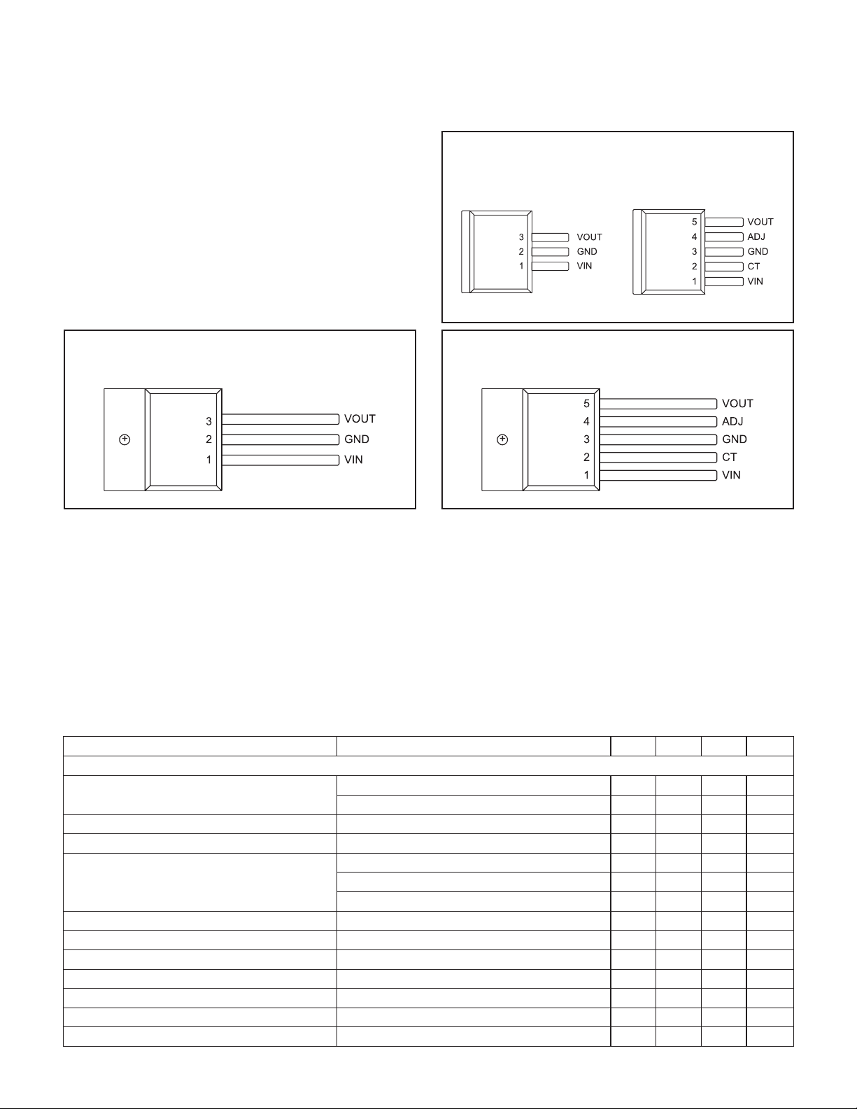
CONNECTION DIAGRAMS
TO-263-3 (Front View)
TD Package
TO-263-5 (Front View)
TD Package
TO-220-3 (Front View)
T Package
TO-220-5 (Front View)
T Package
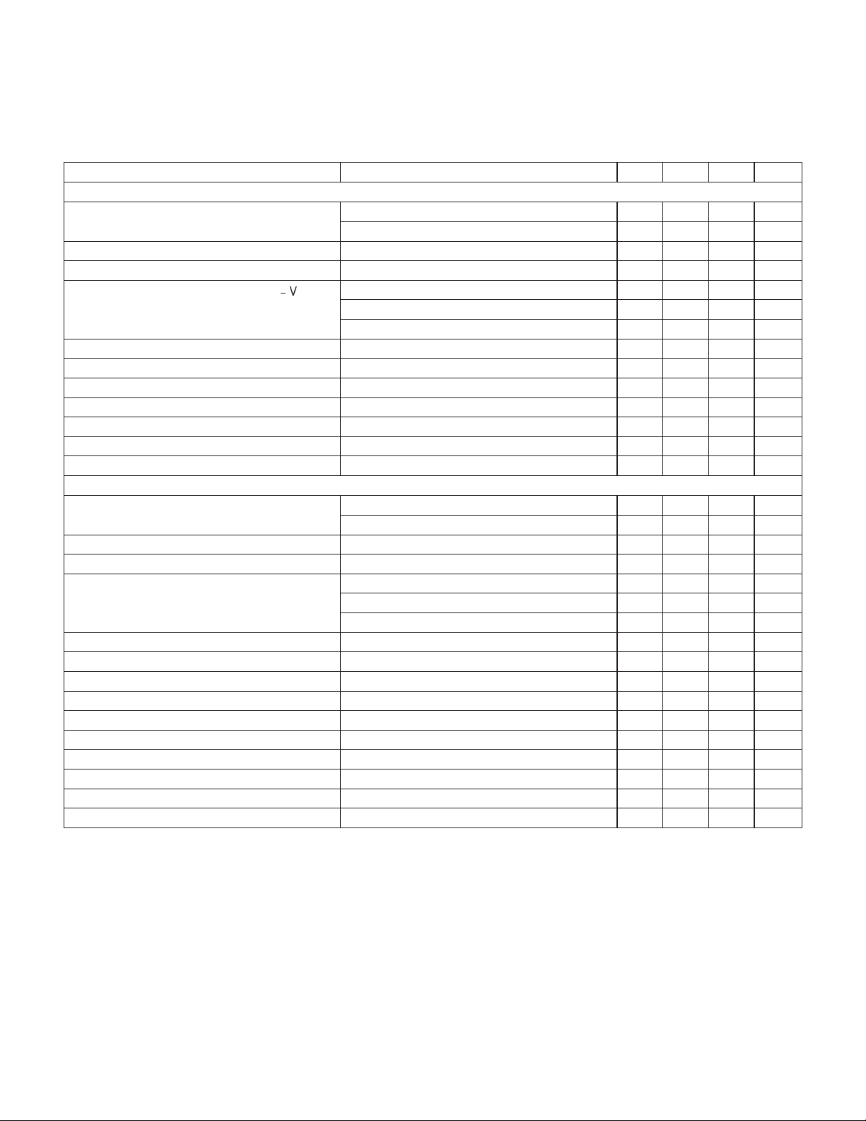
ELECTRICAL CHARACTERISTICS: Unless otherwise stated, these specifications hold for T
A
=0°Cto70°C for the
UCC383-X series, −40°C to +85°C for the UCC283-X, V
VIN
=V
VOUT
+ 1.5V, I
OUT
= 10mA, C
IN
=10µF, C
OUT
=22µF. For the
283-ADJ, V
VIN
= 6.5V, CT = 750pF, T
J
=T
A
.
PARAMETER TEST CONDITIONS MIN TYP MAX UNITS
UCC283-5 Fixed 5V, 3A Family
Output Voltage T
J
=25°C 4.925 5 5.075 V
Over Temperature 4.875 5.125 V
Line Regulation V
VIN
= 5.15V to 9V 2 10 mV
Load Regulation I
OUT
= 10mA to 3A 10 20 mV
Dropout Voltage, V
DROPOUT
=V
VIN
− V
VOUT
I
OUT
= 3A, VOUT = 4.85V 0.4 0.6 V
I
OUT
= 1.5A, VOUT = 4.85V 0.2 0.45 V
I
OUT
= 10mA, VOUT = 4.85V 50 150 mV
Peak Current Limit V
VOUT
= 0V 4 5 6.5 A
Overcurrent Threshold 3 4 5.5 A
Current Limit Duty Cycle V
VOUT
=0V 3 5 %
Overcurrent Time Out, T
ON
V
VOUT
= 0V 400 750 1400 µs
Quiescent Current No load 400 650 µA
Reverse Leakage Current 0V < V
VIN
<V
VOUT
,
V
VOUT
≤ 5.1V, at V
VOUT
075mA
UVLO VIN where VOUT passes current 2.6 2.8 3 V
See Note 1
See Note 1See Note 1
Note 1: Tab = GND
3
UCC283-3/-5/-ADJ
UCC383-3/-5/-ADJ
ELECTRICAL CHARACTERISTICS:
Unless otherwise stated, these specifications hold for T
A
=0°Cto70°C for the
UCC383-X series, −40°C to +85°C for the UCC283-X, V
VIN
=V
VOUT
+ 1.5V, I
OUT
= 10mA, C
IN
=10µF, C
OUT
=22µF. For the
283-ADJ, V
VIN
= 6.5V, CT = 750pF, T
J
=T
A
.
PARAMETER TEST CONDITIONS MIN TYP MAX UNITS
UCC283-3 Fixed 3.3V, 3A Family
Output Voltage T
J
=25°C 3.25 3.3 3.35 V
Over Temperature 3.22 3.38 V
Line Regulation V
VIN
= 3.45V to 9V 2 7 mV
Load Regulation I
OUT
= 10mA to 3A 7 15 mV
Dropout Voltage, V
DROPOUT
=V
VIN
-
V
VOUT
I
OUT
= 3A, VOUT = 3.15V 0.5 1 V
I
OUT
= 1.5A, VOUT = 3.15V 0.25 0.6 V
I
OUT
= 10mA, VOUT = 3.15V 50 150 mV
Peak Current Limit V
VOUT
= 0V 4 5 6.5 A
Overcurrent Threshold 3 4 5.5 A
Current Limit Duty Cycle V
VOUT
=0V 3 5 %
Overcurrent Time Out, TON V
VOUT
= 0V 400 750 1400 µs
Quiescent Current No load 400 650 µA
Reverse Leakage Current 0V < V
VIN
<V
VOUT
,
V
VOUT
≤ 3.35V, at V
VOUT
075mA
UVLO VIN where VOUT passes current 2.6 2.8 3 V
UCC283-ADJ Adjustable Output, 3A Family
Regulating Voltage at ADJ Pin T
J
= 25°C 1.23 1.25 1.27 V
Over Temperature 1.22 1.28 V
Line Regulation, at ADJ Input V
VIN
=V
VOUT
+ 150mV to 9V 1 3 mV
Load Regulation, at ADJ Input I
OUT
= 10mA to 3A 2 5 mV
Dropout Voltage, V
DROPOUT
= VIN − VOUT V
VIN
> 4V, I
OUT
= 3A 0.4 0.6 V
V
VIN
> 3V, I
OUT
= 1.5A 0.2 0.45 V
V
VIN
> 3V, I
OUT
= 10mA 50 150 mV
Peak Current Limit V
VOUT
= 0V, VIN = 6.5V 4 5 6.5 A
Overcurrent Threshold V
VIN
= 6.5V 3 4 5.5 A
Current Limit Duty Cycle V
VOUT
=0V 3 5 %
Overcurrent Time Out, T
ON
V
VOUT
= 0V, CT = 1500pF 750 µs
Reverse Leakage Current 0V < V
VIN
<V
VOUT
,
V
VOUT
≤ 9V, at V
VOUT
0 100 mA
Bias current at ADJ Input 100 250 nA
Quiescent Current No load 400 650 µA
Shutdown Threshold At CT Input 0.25 0.45 V
Quiescent Current in Shutdown V
VIN
= 10V 40 75 µA
UVLO VIN where VOUT passes current 2.6 2.8 3 V
 Loading...