


Texas Instruments UC3725N, UC3725DWTR, UC3725DW, UC2725J, UC1725L Datasheet
...
UC1725
UC2725
UC3725
Isolated High Side FET Driver
FEATURES
∙Receives Both Power and Signal Across the Isolation Boundary
∙9 to 15 Volt High Level Gate Drive
∙Under-voltage Lockout
∙Programmable Over-current Shutdown and Restart
∙Output Enable Function
DESCRIPTION
The UC1725 and its companion chip, the UC1724, provide all the necessary features to drive an isolated MOSFET transistor from a TTL input signal. A unique modulation scheme is used to transmit both power and signals across an isolation boundary with a minimum of external components.
Protection circuitry, including under-voltage lockout, over-current shutdown, and gate voltage clamping provide fault protection for the MOSFET. High level gate drive is guaranteed to be greater than 9 volts and less than 15 volts under all conditions.
Uses include isolated off-line full bridge and half bridge drives for driving motors, switches, and any other load requiring full electrical isolation.
The UC1725 is characterized for operation over the full military temperature range of -55°C to +125°C while the UC2725 and UC3725 are characterized for -25°C to +85°C and 0°C to +70°C respectively.
BLOCK DIAGRAM
UDG-92051-1 |
1/94 |
ABSOLUTE MAXIMUM RATINGS
Supply Voltage (pin 3) . . . . . . . . . . . . . . . . . . . . . . . . . . . . . 30V Power inputs (pins 7 & 8) . . . . . . . . . . . . . . . . . . . . . . . . . . . 30V Output current, source or sink (pin 2)
DC. . . . . . . . . . . . . . . . . . . . . . . . . . . . . . . . . . . . . . . . . . . . 0.5A Pulse (0.5 us) . . . . . . . . . . . . . . . . . . . . . . . . . . . . . . . . . . . 2.0A Enable and Current limit inputs (pins 4 & 6). . . . . . . . -0.3 to 6V Power Dissipation at TA ≤ 25°C (DIL-8) . . . . . . . . . . . . . . . . 1W Power Dissipation at TA ≤ 25°C (SO-14) . . . . . . . . . . . . 725mW Lead Temperature (Soldering, 10 Seconds) . . . . . . . . . . 300°C
Note 1: Unless otherwise indicated, voltages are referenced to ground and currents are positive into, negative out of, the specified terminals (pin numbers refer to DIL-8 package).
Note 2: See Unitrode Integrated Circuits databook for information regarding thermal specifications and limitations of packages.
UC1725
UC2725
UC3725
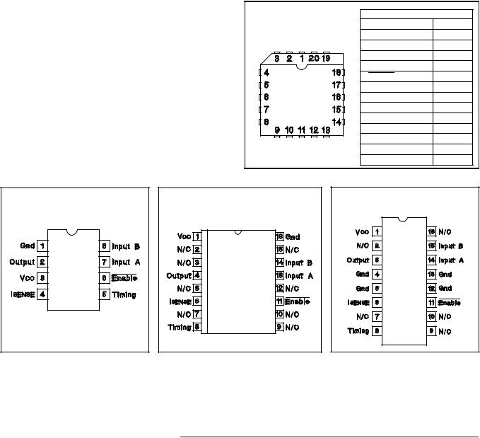
CONNECTION DIAGRAMS
PLCC-20 (Top View) |
PACKAGE PIN FUNCTION |
||
FUNCTION |
PIN |
||
Q Package |
|||
N/C |
1 |
||
|
|||
|
ISENSE |
2 |
|
|
N/C |
3-5 |
|
|
Timing |
6 |
|
|
Enable |
7 |
|
|
N/C |
8-9 |
|
|
Input A |
11 |
|
|
N/C |
12-14 |
|
|
Input B |
15 |
|
|
Gnd |
16 |
|
|
VCC |
17 |
|
|
N/C |
18-19 |
|
|
Output |
20 |
|
DIL-8 (Top View) |
J Or N Package |
SOIC-16 (Top View) |
DW Package |
DIL-16 (Top View)
JE Or NE Package
ELECTRICAL CHARACTERISTICS: (Unless otherwise stated, these specifications apply for -55°C≤TA≤+125°C for UC1725; -25°C≤TA≤+85°C for UC2725; 0°C≤TA≤+70°C for UC3725; VCC (pin 3) =
0 to 15V, RT=10k, CT=2.2nf, TA =TJ, pin numbers refer to DIL-8 package.)
PARAMETER |
TEST CONDITIONS |
MIN |
TYP |
MAX |
UNITS |
POWER INPUT SECTION (PINS 7 & 8) |
|
|
|
|
|
Forward Diode Drop, Schottky Rectifier |
IF = 50ma |
|
.55 |
.7 |
V |
|
IF = 500ma |
|
1.1 |
1.5 |
V |
CURRENT LIMIT SECTION (PIN 4) |
|
|
|
|
|
Input bias current |
VPIN4 = OV |
|
-1 |
-10 |
μA |
Threshold voltage |
|
0.4 |
0.5 |
0.6 |
V |
Delay to outputs |
VPIN4 = 0 to 1V |
|
100 |
250 |
ns |
TIMING SECTION (PIN 5) |
|
|
|
|
|
Output Off Time |
|
27 |
30 |
33 |
μs |
Upper Mono Threshold |
|
6.3 |
7.0 |
7.7 |
V |
Lower Mono Threshold |
|
1.9 |
2.0 |
2.3 |
V |
HYSTERESIS AMPLIFIER (PINS 7 & 8) |
|
|
|
|
|
Input Open Circuit Voltage |
Inputs (pins 7 & 8), Open Circuited, TA= 25°C |
7.0 |
Vcc/2 |
8.0 |
V |
Input Impedance |
TA = 25°C |
23 |
28 |
33 |
kΩ |
Hysteresis |
|
26.5 |
2*Vcc |
30.5 |
V |
Delay to Outputs |
VPIN7 - VPIN8 = VCC + 1V |
|
100 |
300 |
ns |
2
 Loading...