


Texas Instruments UC3823N, UC3823J, UC3823DWTR, UC3823DW, UC3823QTR Datasheet
...
UC1823
UC2823
UC3823
High Speed PWM Controller
FEATURES
∙Compatible with Voltage or Current-Mode Topologies
∙Practical Operation @ Switching Frequencies to 1.0MHz
∙50ns Propagation Delay to Output
∙High Current Totem Pole Output (1.5A peak)
∙Wide Bandwidth Error Amplifier
∙Fully Latched Logic with Double Pulse Suppression
∙Pulse-by-Pulse Current Limiting
∙Soft Start/Max. Duty Cycle Control
∙Under-Voltage Lockout with Hysteresis
∙Low Start Up Current (1.1mA)
∙Trimmed Bandgap Reference (5.1V ±1%)
DESCRIPTION
The UC1823 family of PWM control ICs is optimized for high frequency switched mode power supply applications. Particular care was given to minimizing propagation delays through the comparators and logic circuitry while maximizing bandwidth and slew rate of the error amplifier. This controller is designed for use in either current-mode or voltage-mode systems with the capability for input voltage feed-forward.
Protection circuitry includes a current limit comparator, a TTL compatible shutdown port, and a soft start pin which will double as a maximum duty cycle clamp. The logic is fully latched to provide jitter free operation and prohibit multiple pulses at the output. An un- der-voltage lockout section with 800mV of hysteresis assures low start up current. During under-voltage lockout, the output is high impedance. The current limit reference (pin 11) is a DC input voltage to the current limit comparator. Consult specifications for details.
These devices feature a totem pole output designed to source and sink high peak currents from capacitive loads, such as the gate of a power MOSFET. The on state is defined as a high level.
ABSOLUTE MAXIMUM RATINGS
Supply Voltage (Pins 15, 13) . . . . . . . . . . . . . . . . . . . . . . . . 30V Output Current, Source or Sink (Pin14)
DC . . . . . . . . . . . . . . . . . . . . . . . . . . . . . . . . . . . . . . . . . . 0.5A Pulse (0.5μs). . . . . . . . . . . . . . . . . . . . . . . . . . . . . . . . . . 2.0A Analog Inputs (Pins 1, 2, 7, 8, 9, 11) . . . . . . . . . . . -0.3V to +6V Clock Output Current (Pin 4) . . . . . . . . . . . . . . . . . . . . . . . -5mA Error Amplifier Output Current (Pin 3) . . . . . . . . . . . . . . . . 5mA Soft Start Sink Current (Pin 8) . . . . . . . . . . . . . . . . . . . . . 20mA
Oscillator Charging Current (Pin 5) . . . . . . . . . . . . . . . . . . -5mA Power Dissipation at TA = 60 °C . . . . . . . . . . . . . . . . . . . . . 1W Storage Temperature Range . . . . . . . . . . . . . . -65°C to +150°C Lead Temperature (Soldering, 10 seconds) . . . . . . . . . . 300°C Note: All voltages are with respect to ground, Pin 10.
Currents are positive into the specified terminal. Consult Packaging Section of Databook for thermal limitations and considerations of packages.
BLOCK DIAGRAM
3/97
1
UC1823
UC2823
UC3823
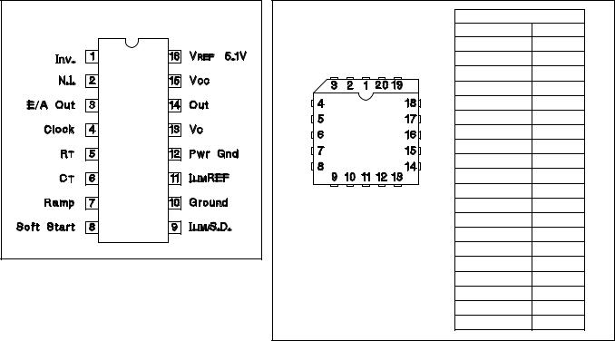
CONNECTION DIAGRAMS
DIL-16, SOIC-16 (TOP VIEW) |
PLCC-20, LCC-20 (TOP VIEW) |
PACKAGE PIN FUNCTION |
|
J or N, DW Package |
Q, L Package |
FUNCTION |
PIN |
|
|
N/C |
1 |
|
|
Inv. |
2 |
|
|
N.I. |
3 |
|
|
E/A Out |
4 |
|
|
Clock |
5 |
|
|
N/C |
6 |
|
|
RT |
7 |
|
|
CT |
8 |
|
|
Ramp |
9 |
|
|
Soft start |
10 |
|
|
N/C |
11 |
|
|
ILIM/S.D. |
12 |
|
|
Ground |
13 |
|
|
ILIM REF |
14 |
|
|
PWR Gnd |
15 |
|
|
N/C |
16 |
|
|
VC |
17 |
|
|
OUT |
18 |
|
|
VCC |
19 |
|
|
VREF 5.1V |
20 |
ELECTRICAL CHARACTERISTICS: Unless otherwise noted, these specifications apply for RT = 3.65k, CT = 1nF, VCC = 15V, 0°C < T A < +70°C for the UC3823, -25°C < T A < +85°C for the UC2823, and -55°C < T A < +125°C for the UC1823, T A = TJ.
|
|
|
UC1823 |
|
|
UC3823 |
|
UNITS |
PARAMETER |
TEST CONDITIONS |
|
UC2823 |
|
|
|
|
|
|
|
MIN |
TYP |
MAX |
MIN |
TYP |
MAX |
|
Reference Section |
|
|
|
|
|
|
|
|
Output Voltage |
TJ = 25°C, l O = 1mA |
5.05 |
5.10 |
5.15 |
5.00 |
5.10 |
5.20 |
V |
Line Regulation |
10 < VCC < 30V |
|
2 |
20 |
|
2 |
20 |
mV |
Load Regulation |
1 < IO < 10mA |
|
5 |
20 |
|
5 |
20 |
mV |
Temperature Stability* |
TMIN < TA < TMAX |
|
0.2 |
0.4 |
|
0.2 |
0.4 |
mV/°C |
Total Output Variation* |
Line, Load, Temp. |
5.00 |
|
5.20 |
4.95 |
|
5.25 |
|
Output Noise Voltage* |
10Hz < f < 10kHz |
|
50 |
|
|
50 |
|
μV |
Long Term Stability* |
TJ = 125°C, 1000 hrs. |
|
5 |
25 |
|
5 |
25 |
mV |
Short Circuit Current |
VREF=0V |
-15 |
-50 |
-100 |
-15 |
-50 |
-100 |
mA |
Oscillator Section |
|
|
|
|
|
|
|
|
Initial Accuracy* |
TJ=25°C |
360 |
400 |
440 |
360 |
400 |
440 |
kHz |
Voltage Stability* |
10 < VCC < 30V |
|
0.2 |
2 |
|
0.2 |
2 |
% |
Temperature Stability* |
TMIN <TA < TMAX |
|
5 |
|
|
5 |
|
% |
Total Variation* |
Line, Temp. |
340 |
|
460 |
340 |
|
460 |
kHz |
Clock Out High |
|
3.9 |
4.5 |
|
3.9 |
4.5 |
|
V |
Clock Out Low |
|
|
2.3 |
2.9 |
|
2.3 |
2.9 |
V |
Ramp Peak* |
|
2.6 |
2.8 |
3.0 |
2.6 |
2.8 |
3.0 |
V |
Ramp Valley* |
|
0.7 |
1.0 |
1.25 |
0.7 |
1.0 |
1.25 |
V |
Ramp Valley to Peak* |
|
1.6 |
1.8 |
2.0 |
1.6 |
1.8 |
2.0 |
V |
* These parameters are guaranteed by design but not 100% tested in production.
2
UC1823
UC2823
UC3823
ELECTRICAL CHARACTERISTICS: Unless otherwise noted, these specifications apply for RT = 3.65k, CT = 1nF, VCC
= 15V, 0°C < T A < +70°C for the UC3823, -25°C < T A < +85°C for the UC2823, and -55°C < T A < +125°C for the UC1823, T A = TJ.
|
|
|
UC1823 |
|
|
UC3823 |
|
UNITS |
PARAMETER |
TEST CONDITIONS |
|
UC2823 |
|
|
|
|
|
|
|
MIN |
TYP |
MAX |
MIN |
TYP |
MAX |
|
Error Amplifier Section |
|
|
|
|
|
|
|
|
Input Offset Voltage |
|
|
|
10 |
|
|
15 |
mV |
Input Bias Current |
|
|
0.6 |
3 |
|
0.6 |
3 |
μA |
Input Offset Current |
|
|
0.1 |
1 |
|
0.1 |
1 |
μA |
Open Loop Gain |
1 < VO < 4V |
60 |
95 |
|
60 |
95 |
|
dB |
CMRR |
1.5 < VCM < 5.5V |
75 |
95 |
|
75 |
95 |
|
dB |
PSRR |
10 < VCC < 30V |
85 |
110 |
|
85 |
110 |
|
dB |
Output Sink Current |
VPIN 3 =1V |
1 |
2.5 |
|
1 |
2.5 |
|
mA |
Output Source Current |
VPIN 3 = 4V |
-0.5 |
-1.3 |
|
-0.5 |
-1.3 |
|
mA |
Output High Voltage |
IPIN 3 = −0.5mA |
4.0 |
4.7 |
5.0 |
4.0 |
4.7 |
5.0 |
V |
Output Low Voltage |
IPIN 3 = 1mA |
0 |
0.5 |
1.0 |
0 |
0.5 |
1.0 |
V |
Unity Gain Bandwidth* |
|
3 |
5.5 |
|
3 |
5.5 |
|
MHz |
Slew Rate* |
|
6 |
12 |
|
6 |
12 |
|
V/μS |
PWM Comparator Section |
|
|
|
|
|
|
|
|
Pin 7 Bias Current |
VPIN 7 = 0V |
|
-1 |
-5 |
|
-1 |
-5 |
μA |
Duty Cycle Range |
|
0 |
|
80 |
0 |
|
85 |
% |
Pin 3 Zero D.C. Threshold |
VPIN 7 = 0V |
1.1 |
1.25 |
|
1.1 |
1.25 |
|
V |
Delay to Output* |
|
|
50 |
80 |
|
50 |
80 |
ns |
Soft-Start Section |
|
|
|
|
|
|
|
|
Charge Current |
VPIN 8 = 0.5V |
3 |
9 |
20 |
3 |
9 |
20 |
μA |
Discharge Current |
VPIN 8 = 1V |
1 |
|
|
1 |
|
|
mA |
Current Limit/Shutdown Section |
|
|
|
|
|
|
|
|
Pin 9 Bias Current |
0 < VPIN 9 < 4V |
|
|
±10 |
|
|
±10 |
μA |
Current Limit Offset |
VPIN 11 = 1.1V |
|
|
15 |
|
|
15 |
mV |
Current Limit Common Mode |
|
1.0 |
|
1.25 |
1.0 |
|
1.25 |
V |
Range (VPIN 11) |
|
|
|
|
|
|
|
|
Shutdown Threshold |
|
1.25 |
1.40 |
1.55 |
1.25 |
1.40 |
1.55 |
V |
Delay to Output* |
|
|
50 |
80 |
|
50 |
80 |
ns |
Output Section |
|
|
|
|
|
|
|
|
Output Low Level |
IOUT = 20mA |
|
0.25 |
0.40 |
|
0.25 |
0.40 |
V |
|
IOUT = 200mA |
|
1.2 |
2.2 |
|
1.2 |
2.2 |
V |
Output High Level |
IOUT = −20mA |
13.0 |
13.5 |
|
13.0 |
13.5 |
|
V |
|
IOUT = −200mA |
12.0 |
13.0 |
|
12.0 |
13.0 |
|
V |
Collector Leakage |
VC = 30V |
|
100 |
500 |
|
100 |
500 |
μA |
Rise/Fall Time* |
CL = 1nF |
|
30 |
60 |
|
30 |
60 |
ns |
Under-Voltage Lockout Section |
|
|
|
|
|
|
|
|
Start Threshold |
|
8.8 |
9.2 |
9.6 |
8.8 |
9.2 |
9.6 |
V |
UVLO Hysteresis |
|
0.4 |
0.8 |
1.2 |
0.4 |
0.8 |
1.2 |
V |
Supply Current |
|
|
|
|
|
|
|
|
Start Up Current |
VCC = 8V |
|
1.1 |
2.5 |
|
1.1 |
2.5 |
mA |
ICC |
VPIN 1, VPIN 7, VPIN 9 =0V, VPIN 2 = 1V |
|
22 |
33 |
|
22 |
33 |
mA |
* These parameters are guaranteed by design but not 100% tested in production.
3
 Loading...