


Texas Instruments UC3851N, UC3851DWTR, UC3851DW, UC2851N, UC2851DWTR Datasheet
...
UC1851
UC2851
UC3851
Programmable, Off-Line, PWM Controller
FEATURES
∙All Control, Driving, Monitoring, and Protection Functions Included
∙Low-Current Off Line Start Circuit
∙Voltage Feed Forward or Current Mode Control
∙High Current Totem Pole Output
∙50% Absolute Max Duty Cycle
∙PWM Latch for Single Pulse Per Period
∙Pulse-by-Pulse Current Limiting plus Shutdown for Over-Current Fault
∙No Start-Up or Shutdown Transients
∙Slow Turn-On Both Initially and After Fault Shutdown
∙Shutdown Upon Over or Under Voltage Sensing
∙Latch Off or Continuous Retry After Fault
∙1% Reference Accuracy
∙500kHz Operation
∙18 Pin DIL or 20 Pin PLCC Package
DESCRIPTION
The UC1851 family of PWM controllers are optimized for offline primary side control. These devices include a high current totem pole output stage and a toggle flip-flop for absolute 50% duty cycle limiting. In all other respects this line of controllers is pin for pin compatible with the UC1841 series. Inclusion of all major housekeeping functions in these high performance controllers makes them ideal for use in cost sensitive applications.
Important features of these controllers include low current start-up, linear feed-forward for constant volt-second operation, and compatibility with both voltage or current mode control. In addition, these devices include a programmable start threshold, as well as programmable over-voltage, under-voltage, and over current fault thresholds. The fault latch on these devices can be configured for automatic restart, or latched off response to a fault.
These devices are packaged in 18-pin plastic or ceramic dual- in-line packages, or for surface mount applications, a 20 Pin PLCC. The UC1851 is characterized for -55°C to +125°C operation while the UC2851 and UC3851 are designed for -40°C to +85°C and 0°C to +70°C, respectively.
BLOCK DIAGRAM
10/94 |
ABSOLUTE MAXIMUM RATINGS (Note 1)
Supply Voltage, +VIN (Pin 15)
Voltage Driven . . . . . . . . . . . . . . . . . . . . . . . . . . . . . . . . +32V Current Driven, 100mA maximum. . . . . . . . . . . Self-limiting PWM Output Voltage (Pin 12) . . . . . . . . . . . . . . . . . . . . . . . 40V PWM Output Current, Steady-State (Pin 12) . . . . . . . . . 400mA PWM Output Peak Energy Discharge . . . . . . . . . . . . 20μJoules Driver Bias Current (Pin 14) . . . . . . . . . . . . . . . . . . . . . -200mA Reference Output Current (Pin 16) . . . . . . . . . . . . . . . . -50mA Slow-Start Sink Current (Pin 8) . . . . . . . . . . . . . . . . . . . . 20mA VIN Sense Current (Pin 11). . . . . . . . . . . . . . . . . . . . . . . . 10mA Current Limit Inputs (Pins 6 & 7) . . . . . . . . . . . . . -0.5 to +5.5V Stop Input (Pin 4) . . . . . . . . . . . . . . . . . . . . . . . . . -0.3 to +5.5V
UC1851
UC2851
UC3851
Comparator Inputs
(Pins 1–7, 9–11, 16). . . . . . . . . . . . . . Internally clamped at 12V Power Dissipation at TA = 25°C (Note 3). . . . . . . . . . . 1000mW Power Dissipation at TC = 25°C (Note 3). . . . . . . . . . . 2000mW Operating Junction Temperature . . . . . . . . . . . -55°C to +150°C Storage Temperature Range . . . . . . . . . . . . . . -65°C to +150°C Lead Temperature (Soldering, 10 sec) . . . . . . . . . . . . . +300°C
Note 1:All voltages are with respect to ground, Pin 13. Currents are positive-into, negative-out of the specified terminal
Note 2:All pin numbers are referenced to DIL-18 package. Note 3:Consult Packaging Section of Databook for thermal
limitations and considerations of package.
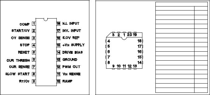
CONNECTION DIAGRAMS
DIL-18, SOIC-18 (TOP VIEW) |
J or N, DW Package |
PLCC-20, LCC-20 |
PACKAGE PIN FUNCTIONS |
|
(TOP VIEW) |
FUNCTION |
PIN |
Q, L PACKAGE |
COMP |
1 |
|
START/UV |
2 |
|
OV SENSE |
3 |
|
STOP |
4 |
|
RESET |
5 |
|
CUR THRESH |
7 |
|
CUR SENSE |
8 |
|
SLOW START |
9 |
|
RT/CT |
10 |
|
RAMP |
11 |
|
VIN SENSE |
12 |
|
PWM OUT |
13 |
|
GROUND |
14 |
|
DRIVE BIAS |
15 |
|
+VIN SUPPLY |
17 |
|
5.0V REF |
18 |
|
INV. INPUT |
19 |
|
N.I. INPUT |
20 |
ELECTRICAL CHARACTERISTICS: Unless otherwise stated, these specifications apply for TA = -55°C to +125°C for the UC1851, -40°C to +85°C for the UC2851, and 0°C to 70°C for the UC3851; V IN =
20V, RT = 20kΩ, CT = .001 mfd, RR = 10kΩ, CR = .001mfd. Current Limit Threshold = 200mV, TA = TJ.
PARAMETER |
TEST CONDITIONS |
UC1851 / UC2851 |
|
UC3851 |
|
UNITS |
|||
MIN |
TYP |
MAX |
MIN |
TYP |
|
MAX |
|
||
|
|
|
|
||||||
Power Inputs |
|
|
|
|
|
|
|
|
|
Start-Up Current |
VIN = 30V, Pin 2 = 2.5V |
|
4.5 |
6 |
|
4.5 |
|
6 |
mA |
Operating Current |
VIN = 30V, Pin 2 = 3.5V |
|
15 |
21 |
|
15 |
|
21 |
mA |
Supply OV Clamp |
VIN = 20mA |
33 |
39 |
45 |
33 |
39 |
|
45 |
V |
Reference Section |
|
|
|
|
|
|
|
|
|
Reference Voltage |
TJ = 25°C |
4.95 |
5.0 |
5.05 |
4.9 |
5.0 |
|
5.1 |
V |
Line Regulation |
VIN = 8 to 30V |
|
10 |
15 |
|
10 |
|
20 |
mV |
Load Regulation |
IL = 0 to 10mA |
|
10 |
20 |
|
10 |
|
30 |
mV |
Total Ref Variation |
Over Operating Temperature Range |
4.9 |
|
5.1 |
4.85 |
|
|
5.15 |
V |
Short Circuit Current |
VREF = 0, TJ = 25°C |
|
-80 |
-100 |
|
-80 |
|
-100 |
mA |
Oscillator |
|
|
|
|
|
|
|
|
|
Nominal Frequency |
TJ = 25°C |
47 |
50 |
53 |
45 |
50 |
|
55 |
kHz |
Voltage Stability |
VIN = 8 to 30V |
|
0.5 |
1 |
|
0.5 |
|
1 |
% |
Total Ref Variation |
Over Operating Temperature Range |
45 |
|
55 |
43 |
|
|
57 |
kHz |
Maximum Frequency |
RT = 2kΩ, CT = 330pF |
500 |
|
|
500 |
|
|
|
kHz |
2
UC1851
UC2851
UC3851
ELECTRICAL CHARACTERISTICS: Unless otherwise stated, these specifications apply for TA = -55°C to +125°C for the UC1851, -40°C to +85°C for the UC2851, and 0°C to 70°C for the UC3851; V IN =
20V, RT = 20kΩ, CT = .001 mfd, RR = 10kΩ, CR = .001mfd. Current Limit Threshold = 200mV, TA = TJ.
PARAMETER |
TEST CONDITIONS |
UC1851 / UC2851 |
|
UC3851 |
|
UNITS |
|||
|
|
MIN |
TYP |
MAX |
MIN |
TYP |
|
MAX |
|
Ramp Generator |
|
|
|
|
|
|
|
|
|
Ramp Current, Minimum |
ISENSE = −10μA |
|
-11 |
-14 |
|
-11 |
|
-14 |
μA |
Ramp Current, Maximum |
ISENSE = 1.0mA |
-0.9 |
-.95 |
|
-0.9 |
-.95 |
|
|
mA |
Ramp Valley |
|
0.3 |
0.4 |
0.6 |
0.3 |
0.4 |
|
0.6 |
V |
Ramp Peak |
Clamping Level |
3.9 |
4.2 |
4.5 |
3.9 |
4.2 |
|
4.5 |
V |
Error Amplifier |
|
|
|
|
|
|
|
|
|
Input Offset Voltage |
VCM = 5.0V |
|
0.5 |
5 |
|
2 |
|
10 |
mV |
Input Bias Current |
|
|
0.5 |
2 |
|
1 |
|
5 |
μA |
Input Offset Current |
|
|
|
0.5 |
|
|
|
0.5 |
μA |
Open Loop Gain |
VO = 1 to 3V |
60 |
66 |
|
60 |
66 |
|
|
dB |
Output Swing (Max Output ≤ |
Minimum Total Range |
0.3 |
|
3.5 |
0.3 |
|
|
3.5 |
V |
Ramp Peak - 100mV) |
|
|
|
|
|
|
|
|
|
CMRR |
VCM = 1.5 to 5.5V |
70 |
80 |
|
70 |
80 |
|
|
dB |
PSRR |
VIN = 8 to 30V |
70 |
80 |
|
70 |
80 |
|
|
dB |
Short Circuit Current |
VCOMP = 0V |
|
-4 |
-10 |
|
-4 |
|
-10 |
mA |
Gain Bandwidth (Note 1) |
TJ = 25°C, AVOL = 0dB |
1 |
2 |
|
1 |
2 |
|
|
MHz |
Slew Rate (Note 1) |
TJ = 25°C, AVCL = 0dB |
|
0.8 |
|
|
0.8 |
|
|
V/μs |
PWM Section |
|
|
|
|
|
|
|
|
|
Continuous Duty Cycle Range |
Minimum Total Continuous Range |
2 |
|
46 |
2 |
|
|
46 |
% |
(other than zero) (Note 1) |
Ramp Peak < 4.2V |
|
|
|
|
|
|
|
|
Output High Level |
ISOURCE = 20mA |
18 |
18.5 |
|
18 |
18.5 |
|
|
V |
|
ISOURCE = 200mA |
17 |
18.5 |
|
17 |
18.5 |
|
|
V |
Rise Time (Note 1) |
TJ = 25°C, CL = 1nF |
|
50 |
150 |
|
50 |
|
150 |
ns |
Fall Time (Note 1) |
TJ = 25°C, CL = 1nF |
|
50 |
150 |
|
50 |
|
150 |
ns |
Output Saturation |
IOUT = 20mA |
|
0.2 |
0.4 |
|
0.2 |
|
0.4 |
V |
|
IOUT = 200mA |
|
1.7 |
2.2 |
|
1.7 |
|
2.2 |
V |
Comparator Delay (Note 1) |
Pin 8 to Pin 12, TJ = 25°C, R L = 1kΩ |
|
300 |
500 |
|
300 |
|
500 |
ns |
Sequencing Functions |
|
|
|
|
|
|
|
|
|
Comparator Thresholds |
Pins 2, 3, 5 |
2.8 |
3.0 |
3.2 |
2.8 |
3.0 |
|
3.2 |
V |
Input Bias Current |
Pins 3, 5 = 0V |
|
-1.0 |
-4.0 |
|
-1.0 |
|
-4.0 |
μA |
Input Leakage |
Pins 3, 5 = 10V |
|
0.1 |
2.0 |
|
0.1 |
|
2.0 |
μA |
Start/UV Hysteresis Current |
Pin 2 = 2.5V |
170 |
200 |
220 |
170 |
200 |
|
230 |
μA |
Ext. Stop Threshold |
Pin 4 |
0.8 |
1.6 |
2.4 |
0.8 |
1.6 |
|
2.4 |
V |
Error Latch Activate Current |
Pin 4 = 0V, Pin 3 > 3V |
|
-120 |
-200 |
|
-120 |
|
-200 |
μA |
Driver Bias Saturation Voltage, |
IB = -50mA |
|
2 |
3 |
|
2 |
|
3 |
V |
VIN-VOH |
|
|
|
|
|
|
|
|
|
Driver Bias Leakage |
VB = 0V |
|
-0.1 |
-10 |
|
-0.1 |
|
-10 |
μA |
Slow-Start Saturation |
IS = 10mA |
|
0.2 |
0.5 |
|
0.2 |
|
0.5 |
V |
Slow-Start Leakage |
VS = 4.5V |
|
0.1 |
2.0 |
|
0.1 |
|
2.0 |
μA |
Current Control |
|
|
|
|
|
|
|
|
|
Current Limit Offset |
|
|
0 |
5 |
|
0 |
|
10 |
mV |
Current Shutdown Offset |
|
370 |
400 |
430 |
360 |
400 |
|
440 |
mV |
Input Bias Current |
Pin 7 = 0V |
|
-2 |
-5 |
|
-2 |
|
-5 |
μA |
Common Mode Range (Note 1) |
|
-0.4 |
|
3.0 |
-0.4 |
|
|
3.0 |
V |
Current Limit Delay (Note 1) |
TJ = 25°C, Pin 7 to 12, RL = 1k |
|
200 |
400 |
|
200 |
|
400 |
ns |
Note 1:Guaranteed by design. Not 100% tested in production.
3
 Loading...