


UCC3626DW
Texas Instruments UCC3626DW, UCC3626PWTR, UCC3626PW, UCC3626N, UCC3626DWTR Datasheet
...
UCC2626
UCC3626
PRELIMINARY
04/99
FEATURES
•
Two Quadrant and Four Quadrant
Operation
•
Integrated Absolute Value Current
Amplifier
•
Pulse-by-Pulse and Average Current
Sensing
•
Accurate, Variable Duty Cycle
Tachometer Output
•
Trimmed Precision Reference
•
Precision Oscillator
•
Direction Output
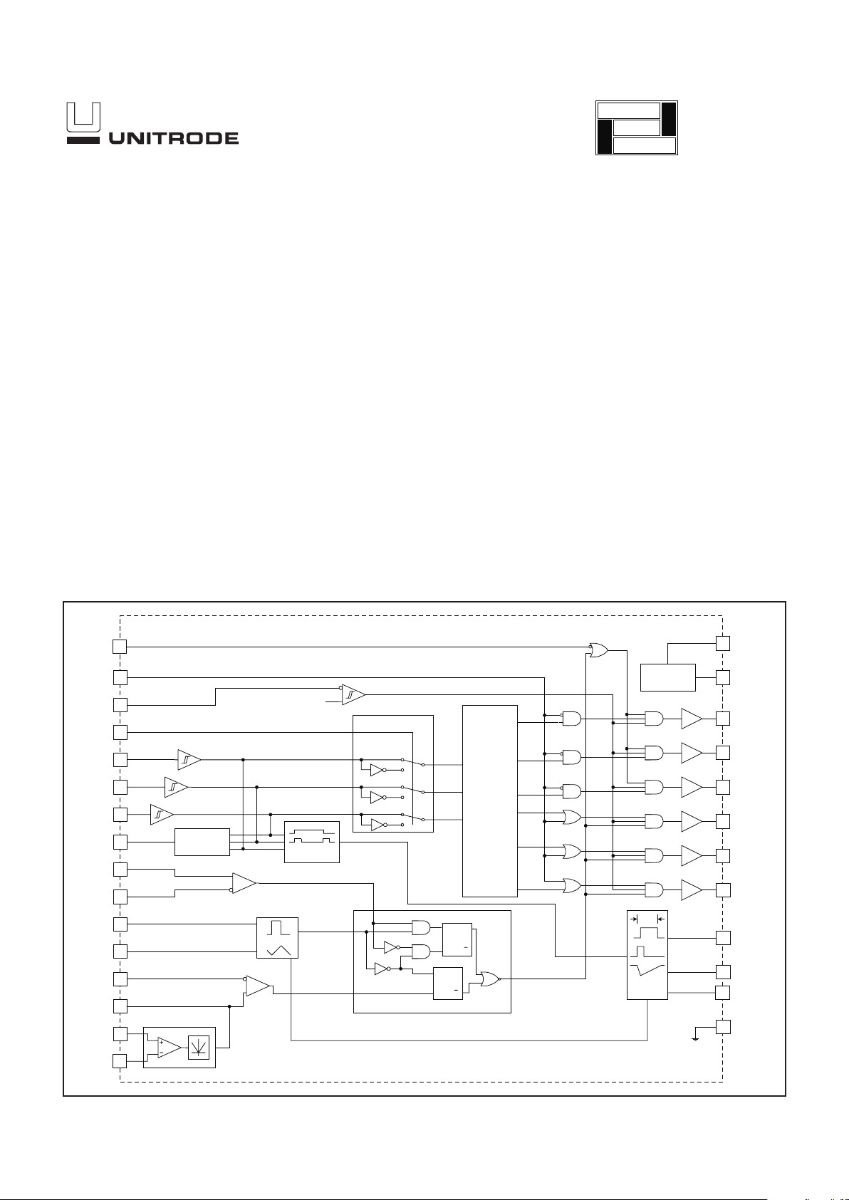
Brushless DC Motor Controller
17HALLC
8DIR_OUT
14PWM_NI
13PWM_I
16HALLB
SYNCH
11
OC_REF
9
SNS_I
3
4
1
5
22 CLOW
C_TACH
R_TACH
TACH_OUT
GND
2VREF
27 AHI
25 BHI
23 CHI
26
ALOW
10
SNS_NI
IOUT
7
6
12
CT
18COAST
21DIR_IN
15HALLA
19BRAKE
20QUAD
SENSE AMPLIFIER
OVER-CURRENT
COMPARATOR
OSCILLATOR
DIRECTION
DETECTOR
EDGE
DETECTOR
28 VDD
ONE SHOT
R•C
5VOLT
REFERENCE
QQSR
PWM LOGIC
24 BLOW
1.75V
DIRECTION
SELECT
HALL
DECODER
PWM COMPARATOR
X5
Q
Q
S
R
BLOCK DIAGRAM
UDG-97173
DESCRIPTION
The UCC3626 motor controller IC combines many of the functions re
quired to design a high performance, two or four quadrant, 3-phase,
brushless DC motor controller into one package. Rotor position inputs
are decoded to provide six outputs that control an external power stage.
A precision triangle oscillator and latched comparator provide PWM mo
tor control in either voltage or current mode configurations. The oscilla
tor is easily synchronized to an external master clock source via the
SYNCH input. Additionally, a QUAD select input configures the chip to
modulate either the low side switches only, or both upper and lower
switches, allowing the user to minimize switching losses in less de
manding two quadrant applications.
The chip includes a differential current sense amplifier and absolute
value circuit which provide an accurate reconstruction of motor current,
useful for pulse by pulse over current protection as well as closing a
current control loop. A precision tachometer is also provided for imple
menting closed loop speed control. The TACH_OUT signal is a variable
duty cycle, frequency output which can be used directly for digital control or filtered to provide an analog feedback signal. Other features include COAST, BRAKE, and DIR_IN commands along with a direction
output, DIR_OUT.
application
INFO
available
2
UCC2626
UCC3626
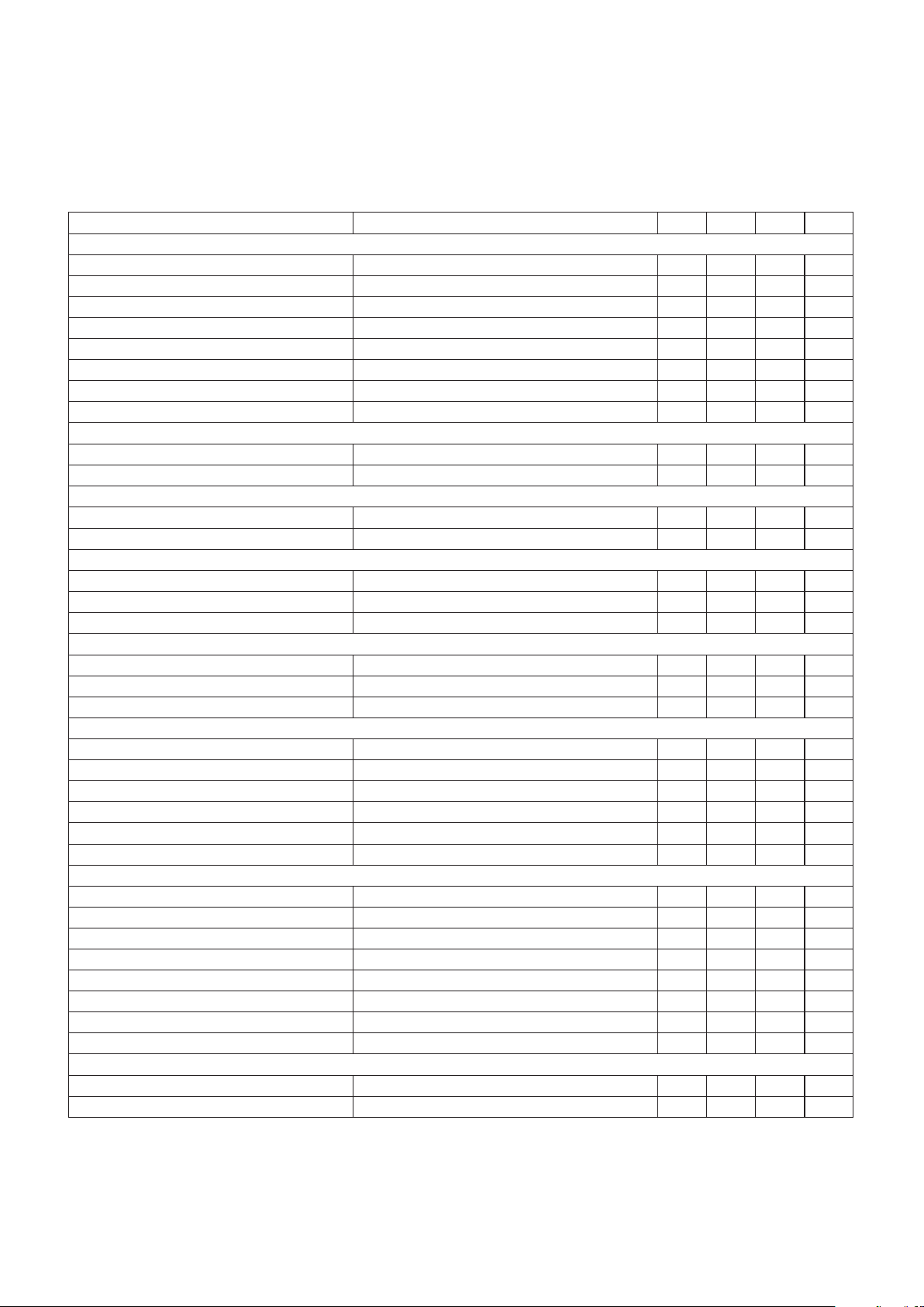
ELECTRICAL CHARACTERISTICS:
Unless otherwise stated, these specifications apply for VCC = 12V; CT = 1nF,
R
TACH
= 250K, C
TACH
= 100pF, TA=TJ, TA= –40°C to +85°C for the UCC2626, and 0°C to +70°C for the UCC3626.
PARAMETER TEST CONDITIONS MIN TYP MAX UNITS
Overall
Supply Current 310mA
Under-Voltage Lockout
Start Threshold 10.5 V
UVLO Hysteresis 0.5 V
5.0 V Reference
Output Voltage I
VREF
= –2mA 4.9 5 5.1 V
Line Regulation 11V < VCC < 14.5V 10 mV
Load Regulation –1 > I
VREF
> –5mA 30 mV
Short Circuit Current 40 120 mA
Coast Input Comparator
Threshold 1.75 V
Hysteresis 0.1 V
Input Bias Current 0.1 µA
IOUT
BHI
ALO
AHI
BRAKE
BLOW
CHI
CLOW
VDD
TACH_OUT
VREF
SNS_I
SYNCH
SNS_NI
R_TACH
C_TACH
CT
GND
DIR_OUT
OC_REF HALLC
DIR_IN
QUAD
COAST
PWM_NI
PWM_I
HALLA
HALLB
14
13
12
11
10
9
8
7
6
5
4
3
2
1
15
16
17
18
19
20
21
22
23
24
25
26
27
28
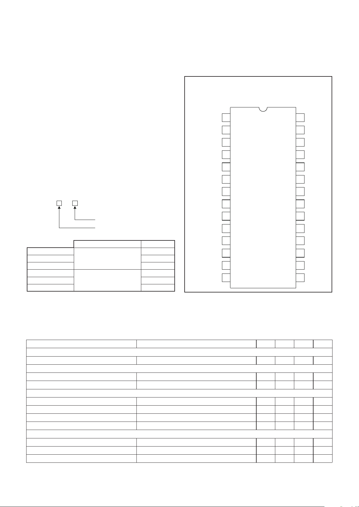
CONNECTION DIAGRAMS
ABSOLUTE MAXIMUM RATINGS
Supply Voltage VDD. . . . . . . . . . . . . . . . . . . . . . . . . . . . . . +15V
Inputs
Pins 20, 19, 18, 21, 15, 16, 17, 7, 12, 9, 10 . . . . –0.3V to V
DD
Pins 13, 14 . . . . . . . . . . . . . . . . . . . . . . . . . . . . –0.3V to 8.0V
Output Current
Pins 22, 23, 24, 25, 26, 27 . . . . . . . . . . . . . . . . . . . . . ±200mA
Pins 2. . . . . . . . . . . . . . . . . . . . . . . . . . . . . . . . . . . . . . –20mA
Pins 3. 8, 11. . . . . . . . . . . . . . . . . . . . . . . . . . . . . . . . . . . 1mA
Storage Temperature . . . . . . . . . . . . . . . . . . . –65°C to +150°C
Junction Temperature. . . . . . . . . . . . . . . . . . . –55°C to +150°C
Lead Temperature (Soldering 10 Seconds). . . . . . . . . . +300°C
Note: Unless otherwise indicated, voltages are referenced to
ground. Currents are positive into, negative out of specified ter
-
minal. Consult packaging section of Databook for thermal limi
-
tations and considerations of package.
DIL-28, SOIC-28, TSSOP-28 (Top View)
N Package, DW Package, PW Package
UCC
PACKAGE
626
TEMPERATURE RANGE
ORDERING INFORMATION
TEMPERATURE RANGE PACKAGE
UCC2626N DIL
UCC2626DW –40° C to +85° C SOIC
UCC2626PW TSSOP
UCC3626N DIL
UCC3626DW 0° C to +70° C SOIC
UCC3626PW TSSOP
3
UCC2626
UCC3626
ELECTRICAL CHARACTERISTICS:
Unless otherwise stated, these specifications apply for VCC = 12V; CT = 1nF,
R
TACH
= 250K, C
TACH
= 100pF, TA=TJ, TA= –40°C to +85°C for the UCC2626, and 0°C to +70°C for the UCC3626.
PARAMETER TEST CONDITIONS MIN TYP MAX UNITS
Current Sense Amplifier
Input Offset Voltage VCM = 0V 5 mV
Input Bias Current VCM = 0V 10 µA
Gain VCM = 0V 4.9 5 5.1 V/V
CMRR –0.3V < VCM < 0.5 60 dB
PSRR 11V < VCC <14.5V 60 dB
Output High Voltage I
IOUT
= –100µA5V
Output Low Voltage I
IOUT
= 100µA50mV
Output Source Current V
IOUT
= 2V 500 µA
PWM Comparator
Input Common Mode Range 2.0 8.0 V
Propogation Delay 75 nS
Over-Current Comparator
Input Common Mode Range 0.0 5.0 V
Propogation Delay 175 nS
Logic Inputs
Logic High QUAD, BRAKE, DIR 3.5 V
Logic Low QUAD, BRAKE, DIR 1.5 V
Input Current QUAD, BRAKE, DIR 0.1 µA
Hall Buffer Inputs
VIL HALLA, HALLB, HALLC 1 V
VIH HALLA, HALLB, HALLC 1.9 V
Input Current 0V < V
IN
< 5V –25 µA
Oscillator
Frequency R
TACH
= 250k, CT = 1nF 10 KHz
Frequency Change With Voltage 12V < VCC < 14.5V 5 %
CT Peak Voltage 7.5 V
CT Valley Voltage 2.5 V
CT Peak-to-Valley Voltage 5.0 V
SYNCH Pin Minimum Pulse Width –500 ns
Tachometer
V
OH/VREF
I
OUT
= –10µA 99 100 %
Vol I
OUT
= 10µA 0 20 mV
R
ON
High I
OUT
= –100µA1kΩ
R
ON
Low I
OUT
= 100µA1kΩ
Ramp Threshold, Lo 20 mV
Ramp Threshold, Hi 2.52 V
C
TACH
Charge Current R
TACH
= 49.9kΩ 50 µA
T-on Accuracy Note 1 –3 3 %
Direction Output
DIR OUT High Level I
OUT
= –100µA 3.5 5.1 V
DIR OUT Low Level I
OUT
= 100µA01V

4
UCC2626
UCC3626
PIN DESCRIPTIONS
AHI, BHI, CHI: Digital outputs used to control the high
side switches in a three phase inverter. For specific de
-
coding information reference Table I.
ALOW, BLOW, CLOW: Digital outputs used to control
the low side switches in a three phase inverter. For specific decoding information reference Table I.
BRAKE: BRAKE is a digital input which causes the device to enter brake mode. In brake mode all three high
side outputs are turned off, AHI, BHI & CHI, while all
three lowside outputs are turned on, ALOW, BLOW,
CLOW. During brake mode the tachometer output remains operational. The only conditions which can inhibit
the low side commands during brake are UVLO, ex
-
ceeding peak current, the output of the PWM compara
-
tor, or the COAST command.
COAST: The COAST input consists of a hysteretic com
parator which disables the outputs. The input is useful in
implementing an overvoltage bus clamp in four quadrant
applications. The outputs will be disabled when the input
is above 1.75V.
CT: This pin is used in conjunction with the R_TACH pin
to set the frequency of the oscillator. A timing capacitor
is normally connected between this point and ground
and is alternately charged and discharged between 2.5V
and 7.5V.
C_TACH: A timing capacitor is connected between this
pin and ground to set the width of the TACH_OUT pulse.
The capacitor is charged with a current set by the resis
tor on pin RT.
DIR_IN: DIR_IN is a digital input which determines the
order in which the HALLA,B & C inputs are decoded. For
specific decode information reference Table I.
DIR_OUT: DIR_OUT represents the actual direction of
the rotor as decoded from the HALLA,B&Cinputs. For
any valid combination of HALLA, B &C inputs there are
two valid transitions, one which translates to a clockwise
rotation and another which translates to a counterclockwise rotation. The polarity of DIR_OUT is the same as
DIR_IN while motoring, i.e. sequencing from top to bottom in Table 1.
GND: GND is the reference ground for all functions of the
part. Bypass and timing capacitors should be terminated
as close to this point as possible.
HALLA, HALLB, HALLC: These three inputs are de
signed to accept rotor position information positioned
120° apart. For specific decode information reference Ta
ble I. These inputs should be externally pulled-up to
VREF or another appropriate external supply.
IOUT: IOUT represents the output of the current sense
and absolute value amplifiers. The output signal appear
ing is a representation of the following expression:
I ABS ISENS I ISENS NI
OUT
=−•(_ _)5
This output can be used to close a current control loop as
well as provide additional filtering of the current sense
signal.
OC_REF: OC_REF is an analog input which sets the trip
voltage of the overcurrent comparator. The sense input of
the comparator is internally connected to the output of the
current sense amplifier and absolute value circuit.
PWM_NI: PWM_NI is the noninverting input to the PWM
comparator.
PWM_I: PWM_I is the inverting input to the PWM com
parator.
ELECTRICAL CHARACTERISTICS: Unless otherwise stated, these specifications apply for VCC = 12V; CT = 1nF,
R
TACH
= 250K, C
TACH
= 100pF, TA=TJ, TA= –40°C to +85°C for the UCC2626, and 0°C to +70°C for the UCC3626.
PARAMETER TEST CONDITIONS MIN TYP MAX UNITS
Output Section
Maximum Duty Cycle 100 %
Output Low Voltage I
OUT
= 10mA 0.4 V
Output High Voltage I
OUT
= –10mA 4.0 5.1 V
Output Low Voltage I
OUT
= 1mA 1 V
Output High Voltage I
OUT
= –1mA 4.0 5.1 V
Rise/Fall Time CI = 100pF 100 nS
Note 1: T(on) is calculated using the formula: T(on) = C
TAC H
(VHI–VLO)/I
CHARGE
. This number is compared to the formula T(on) =
R
TAC H
C
TAC H
.

5
UCC2626
UCC3626
Table 1 provides the decode logic for the six outputs,
AHI, BHI, CHI, ALOW, BLOW, and CLOW as a function
of the BRAKE, COAST, DIR_IN, HALLA, HALLB, and
HALLC inputs.
The UCC3626 is designed to operate with 120° position
sensor encoding. In this format, the three position sensor
signals are never simultaneously high or low. Motor's
whose sensors provide 60° encoding can be converted
to 120° using the circuit shown in Fig. 1.
In order to prevent noise from commanding improper
commutation states, some form of low pass filtering on
HALLA, HALLB, and HALLC is recommended. Passive
APPLICATION INFORMATION
QUAD: The QUAD input selects between “two” QUAD =
0 and “four” QUAD = 1 quadrant operation. When in
“two-quadrant” mode only the low side devices are ef
fected by the output of the PWM comparator. In
“four-quadrant” mode both high and low side devices are
controlled by the PWM comparator.
SYNCH: The SYNCH input is used to synchronize the
PWM oscillator with an external digital clock. When using
the SYNCH feature, a resistor equal to R
TA CH
must be
placed in parallel with CT. When not used, ground
SYNCH.
SNS_NI, SNS_I: These inputs are the noninverting and
inverting inputs to the current sense amplifier, respec
tively. The integrated amplifier is configured for a gain of
five. An absolute value function is also incorporated into
the output in order to provide a representation of actual
motor current when operating in four quadrant mode.
TACH_OUT: TACH_OUT is the output of a monostable
triggered by a change in the commutation state, thus pro
viding a variable duty cycle, frequency output. The
on-time of the monostable is set by the timing capacitor
connected to C_TACH. The monostable is capable of be
ing retriggered if a commutation occurs during it's
on-time.
R_TACH: A resistor connected between R_TACH and
ground programs the current for both the oscillator and
tachometer.
VDD: VDD is the input supply connection for this device.
Undervoltage lockout keeps the outputs off for inputs be
low 10.5V. The input should be bypassed with a 0.1µFce
ramic capacitor, minimum.
VREF: VREF is a 5V, 2% trimmed reference output with
5mA of maximum available output current. This pin
should be bypassed to ground with a 0.1µF ceramic ca
pacitor, minimum.
PIN DESCRIPTIONS (cont.)
B
R
A
K
E
C
O
A
S
T
D
I
R
_
IN
HALL
INPUTS
HIGH SIDE
OUTPUTS
LOW SIDE
OUTPUTS
ABCABCABC
001101100010
001100100001
001110010001
001010010100
001011001100
001001001010
000101010100
000001010001
000011100001
000010100010
000110001010
000100001100
X1XXXX000000
10XXXX000111
00X111000000
00X000000000
Table 1. Commutation truth table.
1kΩ
2N2222A
1kΩ
1kΩ
1kΩ
VREF
VREF
VREF
HALLB
HALLA
HALLC
HALLA
HALLB
HALLC
2.2nF
2.2nF
2.2nF
499Ω
499Ω
Figure 1. Circuit to convert 60° hall code to 120°
code.
 Loading...