


UCC1806L883B
UCC1806
UCC2806
UCC3806
Low Power, Dual Output, Current Mode PWM Controller
FEATURES
• BiCMOS Version of UC1846 Families
• 1.4mA Maximum Operating Current
• 100µA Maximum Startup Current
• 1.0A Peak Output Current
• 125nsec Circuit Delay
• Easier Parallelability
• Improved Benefits of Current Mode
Control
DESCRIPTION
The UCC1806 family of BiCMOS PWM controllers offers exceptionally im-
proved performance with a familiar architecture. With the same block dia-
gram and pinout of the popular UC1846 series, the UCC1806 line features
increased switching frequency capability while greatly reducing the bias
current used within the device. With a typical startup current of 50µA and a
well defined voltage threshold for turn-on, these devices are favored for ap-
plications ranging from off-line power supplies to battery operated portable
equipment. Dual high current, FET driving outputs and a fast current sense
loop further enhance device versatility.
All the benefits of current mode control including simpler loop closing, volt-
age feed-forward, parallelability with current sharing, pulse-by-pulse current
limiting, and push-pull symmetry correction are readily achievable with the
UCC1806 series.
(continued)
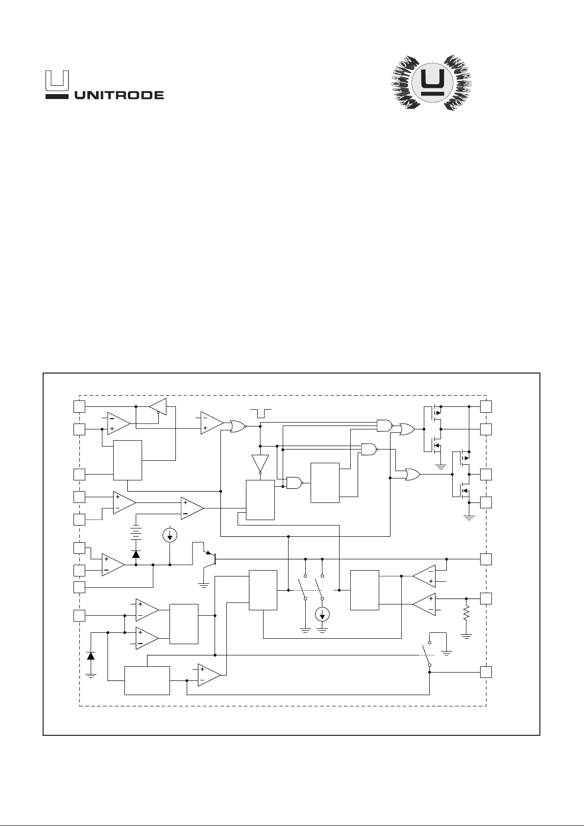
10
7
3
8
SYNC
9RT
4.4V 1.5V
OSC
LO
CT
3X
4
5
EA
6
120µA
1
S
1
QB
R
S
2
13 VC
11 AOUT
14 BOUT
12 GND
T
Q
QB
SHUTDOWN
LOCK OUT
S
1
Q
R
S
2
200µA
Q
R
S
16
200k
1.00V
0.35V
Q
R
S
CURRENT LIMIT
RESTART
UNDER VOLTAGE LOCKOUT
15
15V
5.1V
REFERENCE
REGULATOR
REFERENCE LOW
4.25V
2
CURLIM
SHUTDOWN
VREF
0.5V
–
+
COMP
7.0V
7.5V
CS–
CS+
NI
INV
COMP
VIN
BLOCK DIAGRAM
02/99
UDG-99035
Pin numbers refer to DIL-16 package.
2
UCC1806
UCC2806
UCC3806
Supply Voltage, Low Impedance (Pin 15) . . . . . . . . . . . . . +15V
Supply Current, High Impedance (Pin 15) . . . . . . . . . . . +25mA
Output Supply Voltage (Pin 13). . . . . . . . . . . . . . . . . . . . . +18V
Output Current, Continuous Source or Sink. . . . . . . . . ±200mA
Output Current, Gate Drive. . . . . . . . . . . . . . . . . . . . . .
±
500mA
Analog Input Voltage (Pin 3, 4, 5, 6, 16) . . −0.3V to +VIN +0.3V
Sync Output Current (Pin 10) . . . . . . . . . . . . . . . . . . . . .
±
30mA
Error Amplifier Output Current (Pin 7) . +10mA/− (Self Limiting)
Power Dissipation at T
A
= 25°C (Note 3). . . . . . . . . . . 1000mW
Power Dissipation at T
C
= 25°C (Note 3). . . . . . . . . . . 2000mW
Storage Temperature Range . . . . . . . . . . . . . . 65°C to +150°C
Lead Temperature (soldering, 10 seconds). . . . . . . . . . +300°Χ
Note 1. All voltages are with respect to Ground, Pin 12.
Note 2. Currents are positive into, negative out of the specified
terminal.
Note 3. Consult packaging section of databook for thermal limi-
ABSOLUTE MAXIMUM RATINGS
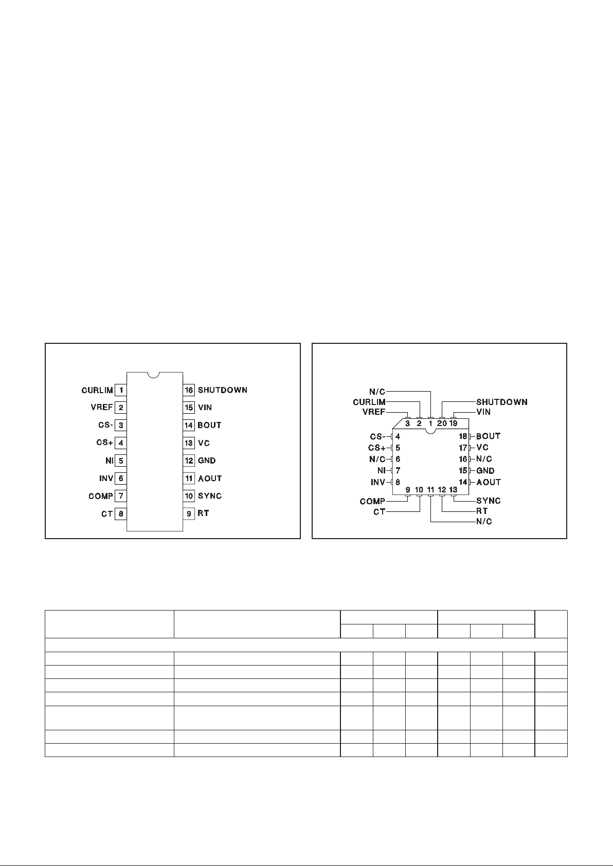
CONNECTION DIAGRAMS
DIL-16 (Top View)
J or N, DW PACKAGE
ELECTRICAL CHARACTERISTICS: Unless otherwise stated, these specifications hold for T
A
= –55°C to +125°C for the
UCC1806, −40°C to +85°C for the UCC2806, and 0°C to +70°C for the UCC3806; V
IN
= 12V, R
T
= 33k, CT = 330pF,
C
BYPASS
on V
REF
= 0.01µF, T
A
= T
J
.
PARAMETER TEST CONDITION UCC1806 / UCC2806 UCC3806 UNITS
MIN TYP MAX MIN TYP MAX
Reference Section
Output Voltage T
J
= 25°C, I
O
= 0.2mA 5.02 5.10 5.17 5.00 5.10 5.20 V
Load Regulation 0.2mA < I
O
< 5mA 3 25 3 25 mV
Temperature Stability (Note 5) 0.2 0.6 0.2 0.6 mV/°C
Total Output Variation Line, Load, Temperature (Note 7) −150 150 −150 150 mV
Output Noise Voltage 10Hz ≤ f ≤ 10kHz, T
J
= 25°C
(Note 5)
70 70 µV
Long Term Stability T
A
= 125°C, 1000 Hours (Note 5) 5 25 5 25 mV
Output Short Circuit −10 −30 −10 −30 mA
PLCC-20, LCC-20 (Top View)
Q, L PACKAGE
These devices are available with multiple package op-
tions for both through-hole and surface mount applica-
tions; and in commercial, industrial, and military
temperature ranges.Contact factory for availability.
The UCC1806 is specified for operation from –55°C to
+125°C, the UCC2806 is specified for operation from
–40°C to +85°C, and the UCC3806 is specified for oper-
ation from 0°C to +70°C. The part is available in DIP and
SOIC packages.
DESCRIPTION (continued)
3
UCC1806
UCC2806
UCC3806
ELECTRICAL CHARACTERISTICS: Unless otherwise stated, these specifications hold for T
A
= –55°C to +125°C for the
UCC1806, −40°C to +85°C for the UCC2806, and 0°C to +70°C for the UCC3806; V
IN
= 12V, R
T
= 33k, CT = 330pF,
C
BYPASS
on V
REF
= 0.01µF, T
A
= T
J
.
PARAMETER TEST CONDITION UCC1806 / UCC2806 UCC3806 UNITS
MIN TYP MAX MIN TYP MAX
Oscillator Section
Initial Accuracy T
J
= 25°C 424752424752kHz
Temperature Stability T
MIN
< T
A
< T
MAX
(Note 5) 2 2 %
Amplitude 2.35 2.35 V
SYNC Delay to Outputs Pin 8 = 0V, Pin 9 = V
REF
,
V
SYNC
= 0.8V to 2.0V
50 125 50 100 ns
Discharge Current T
J
= 25°C, V
PIN
8 = 2.0V 2 2 mA
SYNC, V
OL
I
OUT
= +1mA 0.4 0.4 V
SYNC, V
OH
I
OUT
= –4mA 2.4 2.4 V
SYNC, V
IL
Pin 8 = 0V, Pin 9 = V
REF
0.8 0.8 V
SYNC, V
IH
Pin 8 = 0V, Pin 9 = V
REF
2.0 2.0 V
SYNC Input Current −1+1−1+1µA
Error Amplifier Section
Input Offset Voltage 5 10 mV
Input Bias Current −1 −1 µA
Input Offset Current 500 500 nA
Common Mode Range 0 V
IN
-2 0 VIN−2V
Open Loop Gain V
O
= 1.0 to 4.0 80 100 80 100 dB
Unity Gain Bandwidth 1 1 MHz
Output Sink Current V
ID
< –20mV, V
PIN 7
= 1.0V 1 1 mA
Output Source Current V
ID
< 20mV, V
PIN 7
= 3.0V −80 −120 −80 −120 µA
Output High Level V
ID
= –50mV 4.5 4.5 V
Output Low Level V
ID
= –50mV 0.5 0.5 V
Current Sense Amplifier Section
Amplifier Gain V
PIN 3
= 0V, V
PIN 1
= V
REF
(Notes 3,4) 2.75 3 3.35 2.75 3 3.35 V/V
Maximum Differential Input
Signal (V
PIN 4 - VPIN 3)
V
PIN 1
= V
REF
, V
PIN 5
= V
REF
,
V
PIN 6
= 0V
1.1 1.1 V
Input Offset Voltage V
PIN 1
= 0.5V, V
PIN 7
= OPEN 10 30 10 50 mV
CMRR V
CM
= 0 to V
IN
– 3.5 60 60 dB
PSRR 56 56 dB
Input Bias Current V
PIN 1
= 0.5V, PIN 7 OPEN (Note 3) −1 −1 µA
Input Offset Current V
PIN 1 = 0.5V, PIN 7 OPEN (Note 3) 1 1 µA
Delay to Outputs V
PIN 5
= V
REF
, PIN 6 = 0, PIN 1 = 2.75V,
PIN 4 – PIN 3 = 0 to 1.5V step (Note 6)
125 175 125 175 ns
Current Limit Adjust Section
Current Limit Offset V
PIN 3
= 0, V
PIN 4
= 0, PIN 7 = open 0.40 0.50 0.60 0.40 0.50 0.60 V
Input Bias Current 11µA
Minimum Latching Current 300 200 300 200 µA
Maximum Non-Latching
Current
200 80 200 80 µA
Shutdown Terminal Section
Threshold Voltage 0.94 1.00 1.06 0.9 1.0 1.1 V
Input Voltage Range 0 V
IN 0VIN V
Delay to Outputs V
PIN 16
= 0 to 1.3V 75 150 75 150 ns
 Loading...