


UCC2882/-1
UCC3882/-1
Average Current Mode Synchronous Controller With 5-Bit DAC
FEATURES
∙Combined DAC/Voltage Monitor and PWM with Synchronous Rectification Functions
∙5-Bit Digital-to-Analog (DAC) Converter
∙1% DAC/Reference Combined Accuracy
∙Compatible with 5V and 12V Systems and 12V-only Systems
∙Low Offset Current Sense Amplifier
∙Programmable Oscillator Frequency Practical to 700kHz
∙Foldback Current Limiting
∙Overvoltage and Undervoltage Fault Windows
∙2Ω Totem Pole Outputs with Programmable Dead Times to Eliminate Cross-Conduction
∙Chip Disable Function
DESCRIPTION
The UCC3882 combines high precision reference and voltage monitoring circuitry with average current mode PWM synchronous rectification controller circuitry to power high-end microprocessors with a minimum of external components. The UCC3882 converts 5V or 12V to an adjustable output ranging from 1.8VDC to 2.05VDC in 50mV steps and 2.1VDC to 3.5VDC in 100mV steps with 1% DC system accuracy.
The DAC output voltage is directly compatible with Intel’s 5-bit VID code (Table 1) which covers 1.3V to 2.05V in 50mV steps and 2.1V to 3.5V in 100mV steps. The accuracy of the DAC/reference combination is better than 1%. Undervoltage lockout circuitry assures the correct logic states at the outputs during power up and power down. The overvoltage and undervoltage comparators monitor the system output voltage and indicate when it rises above or falls below its designed value by more than 9%. A second overvoltage comparator digitally forces GATEHI off and GATELO on when the system output voltage exceeds its designed value by more than 17.5%.
(continued)
BLOCK DIAGRAM
UDG-97047-1 |
03/99 |
UCC2882/-1
UCC3882/-1
ABSOLUTE MAXIMUM RATINGS |
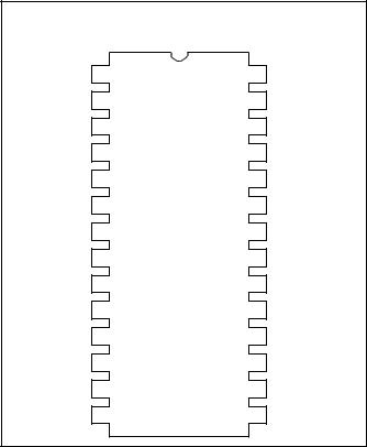
CONNECTION DIAGRAM |
VDRVHI, GATEHI (Note 1) . . . . . . . . . . . . . . . . . –0.3V to 20V VDRVLO, GATELO. . . . . . . . . . . . . . . . . . . . . . . . –0.3V to 15V All other pins referenced to GND . . . . . . . . . . . . . –0.3V to 5.3V VIN. . . . . . . . . . . . . . . . . . . . . . . . . . . . . . . . . . . . . . . . . . . +15V Storage Temperature . . . . . . . . . . . . . . . . . . . –65°C to +150°C Junction Temperature. . . . . . . . . . . . . . . . . . . –55°C to +150°C Lead Temperature (Soldering, 10 sec.) . . . . . . . . . . . . . +300°C
Currents are positive into, negative out of the specified terminal. Consult Packaging Section of Databook for thermal limitations and considerations of packages.
Note 1: 20V at no load. Derate to 18.5V when used with capacitive loads of greater than 1000pF in series with less than 20 Ω.
DIL-28, SOIC-28 (Top View)
N, DW or PW Packages
VSNS |
1 |
28 |
GND |
PWRGD |
2 |
27 |
D0 |
N/C |
3 |
26 |
D1 |
CAM |
4 |
25 |
N/C |
CAO |
5 |
24 |
D2 |
ISOUT |
6 |
23 |
D3 |
IS+ |
7 |
22 |
D4 |
IS– |
8 |
21 |
VREF |
VIN |
9 |
20 |
COMMAND |
VDRVLO |
10 |
19 |
VDRVHI |
GATELO |
11 |
18 |
GATEHI |
PGND |
12 |
17 |
EN |
RT |
13 |
16 |
COMP |
CT |
14 |
15 |
VFB |
DESCRIPTION (continued)
For all of the parts, grounding the EN pin disables the GATEHI and GATELO outputs, shutting down the power supply. For the 2882 and 3882 only, programming a DAC output voltage below 1.8V, or programming all of the VID pins high also disables the GATEHI and GATELO outputs. For the “–1" option parts, the GATEHI and GATELO outputs are switching, and the power supply output voltage regulates at the programmed DAC output voltage for all VID codes.
The voltage and current amplifiers have 2.5MHz gain-bandwidth product to satisfy high performance system requirements. The internal current sense amplifier permits the use of a low value current sense resistor, minimizing power loss. The oscillator frequency is exter-
nally programmed with RT and CT. The foldback circuit reduces the converter short circuit current limit to 50% of its nominal value when the converter is short-circuited, minimizing component stress and dissipation during abnormal conditions. The gate drivers are low impedance totem pole output stages capable of driving large external MOSFETs. Cross conduction is eliminated internally by programming the dead time between turn-off and turn on of the external high side and synchronous MOSFETs.
This device is available in a 28-pin wide body surface mount package. The UCC2882 is specified for operation from –25°C to +85°C and the UCC3882 is specified for operation from 0°C to 70°C.
ELECTRICAL CHARACTERISTICS: Unless otherwise specified, VIN = VDRVHI = VDRVLO = 12V, VSNS = 3.5V, VD0 = VD1 = VD2 = VD3 = VD4 = 0V, RT = 13k, CT = 1.8nF, EN = Open, 0°C < T A < 70°C, T A = TJ.
PARAMETER |
TEST CONDITIONS |
MIN |
TYP |
MAX |
UNITS |
Undervoltage Lockout |
|
|
|
|
|
VIN UVLO Turn-on Threshold |
|
|
10.5 |
10.8 |
V |
VIN UVLO Turn-off Threshold |
|
9.5 |
10 |
|
V |
UVLO Threshold Hysteresis |
|
300 |
500 |
700 |
mV |
Supply Current |
|
|
|
|
|
lIN |
EN = 0V |
|
7 |
12 |
mA |
2
UCC2882/-1
UCC3882/-1
ELECTRICAL CHARACTERISTICS: Unless otherwise specified, VIN = VDRVHI = VDRVLO = 12V, VSNS = 3.5V, VD0 = VD1 = VD2 = VD3 = VD4 = 0V, RT = 13k, CT = 1.8nF, EN = Open, 0°C < T A < 70°C, T A = TJ.
PARAMETER |
TEST CONDITIONS |
MIN |
TYP |
MAX |
UNITS |
DAC/Reference |
|
|
|
|
|
COMMAND Voltage Accuracy |
10.8V < VIN < 13.2V, IREF = 0mA (Note 1) |
–1 |
|
1 |
% |
D0-D4 Voltage High |
DX Pin Floating |
|
5 |
5.2 |
V |
D0-D4 Input Bias Current |
DX Pin Tied to GND |
–120 |
–70 |
–20 |
μA |
OVP Comparator |
|
|
|
|
|
Trip Point |
% Over COMMAND Voltage (Note 2) |
10 |
17 |
25 |
% |
Hysteresis |
|
|
20 |
|
mV |
OV Comparator |
|
|
|
|
|
Trip Point |
% Over COMMAND Voltage (Note 2) |
5 |
9 |
12 |
% |
Hysteresis |
|
|
20 |
|
mV |
PWRGD On Resistance |
|
|
|
470 |
Ω |
UV Comparator |
|
|
|
|
|
Trip Point |
% Over COMMAND Voltage (Note 2) |
–12 |
–9 |
–5 |
% |
Hysteresis |
|
|
20 |
|
mV |
Enable Pin |
|
|
|
|
|
Pull Up Current |
VEN = 2.5V |
–80 |
–50 |
–20 |
μA |
Voltage Error Amplifier |
|
|
|
|
|
Input Offset Voltage |
VCM = 3V |
–10 |
0 |
10 |
mV |
Input Bias Current |
VCM = 3V |
–0.5 |
|
0.5 |
μA |
Open Loop Gain |
2.05V < VCOMP < 3.05V |
|
90 |
|
dB |
Power Supply Rejection Ratio |
10.8V < VIN < 15V |
|
85 |
|
dB |
Output Sourcing Current |
VVFB = 2V, VCOMMAND = VCOMP = 2.5V |
|
–1.6 |
–0.8 |
mA |
Output Sinking Current |
VVFB = 3V, VCOMMAND = VCOMP = 2.5V |
|
1 |
|
mA |
Current Sense Amplifier |
|
|
|
|
|
Gain |
|
15 |
16 |
17 |
V/V |
Common Mode Rejection Ratio |
0V < VCM < 4.5V |
|
60 |
|
dB |
Power Supply Rejection Ratio |
10.8V < VIN < 15V |
|
80 |
|
dB |
Output Sourcing Current |
VIS– = 2V, VISOUT = VIS+ = 2.5V |
|
–4 |
–3 |
mA |
Output Sinking Current |
VIS– = 3V, VISOUT = VIS+ = 2.5V |
3 |
4 |
|
mA |
Current Amplifier |
|
|
|
|
|
Input Offset Voltage |
VCM = 3V |
|
1 |
|
mV |
Input Bias Current |
VCM = 3V |
|
–0.1 |
|
μA |
Open Loop Gain |
1V < VCAO < 2.5V |
|
90 |
|
dB |
Output Voltage High |
|
|
3 |
|
V |
Power Supply Rejection Ratio |
10.8V < VIN < 15V |
|
80 |
|
dB |
Output Sourcing Current |
VCAM = 2V, VCAO = VCOMP = 2.5V |
|
–7 |
|
mA |
Output Sinking Current |
VCAM = 3V, VCAO = VCOMP = 2.5V |
|
17 |
|
mA |
Oscillator |
|
|
|
|
|
Initial Accuracy |
TA = 25°C |
324 |
360 |
396 |
kHz |
|
0°C < T A < 70°C |
300 |
360 |
420 |
kHz |
Valley to Peak Voltage |
|
|
1.67 |
|
V |
Frequency Change With Voltage |
10.8V < VIN < 15V |
|
1 |
|
% |
Output Section (GATEHI and GATELO) |
|
|
|
|
|
Output Low Voltage |
IGATE = –100mA |
|
0.2 |
|
V |
Output High Voltage |
IGATE = 100mA |
|
11.8 |
|
V |
Rise Time |
CGATE = 3.3nF, RSERIES = 10Ω |
|
20 |
80 |
ns |
Fall Time |
CGATE = 3.3nF, RSERIES = 10Ω |
|
15 |
80 |
ns |
3
UCC2882/-1
UCC3882/-1
ELECTRICAL CHARACTERISTICS: Unless otherwise specified, VIN = VDRVHI = VDRVLO = 12V, VSNS = 3.5V, VD0 = VD1 = VD2 = VD3 = VD4 = 0V, RT = 13k, CT = 1.8nF, EN = Open, 0°C < T A < 70°C, T A = TJ.
PARAMETER |
TEST CONDITIONS |
MIN |
TYP |
MAX |
UNITS |
Turn On Delay |
|
|
|
|
|
GATEHI Turn Off to GATELO Turn On |
|
|
150 |
|
ns |
GATELO Turn Off to GATEHI Turn On |
|
|
135 |
|
ns |
Foldback Current Limit |
|
|
|
|
|
Clamp Level |
VCOMMAND = VSNS |
|
1.37 |
|
V |
|
VFB = VCOMMAND – 100mV (Note 3) |
|
|
|
|
|
VSNS = 0 |
|
0.71 |
|
V |
|
VFB = VCOMMAND – 100mV (Note 3) |
|
|
|
|
System Short Circuit Current Limit |
VCOMMAND = 2.3V |
14.4 |
17 |
22 |
A |
|
VFB = 0V (Note 4) |
|
|
|
|
Note 1: This test measures the combined errors of the COMMAND voltage and the voltage amplifier offset voltage. Applies to all DAC codes from 1.8V to 3.5V.
Note 2: This percentage is measured with respect to the ideal COMMAND voltage programmed by the D0 - D4 pins. Note 3: This voltage is measured with respect to the COMMAND voltage.
Note 4: The calculation of this parameter assumes an offchip sense resistor value of 0.005Ω. This test encompasses all sources of error from the IC.
PIN DESCRIPTIONS
CAM: This pin is the inverting input to the current amplifier. The average load current feedback from the ISOUT pin is applied through a resistor to this pin. The current loop compensation network is also connected to this pin (see CAO below).
CAO: This pin is the current amplifier output. The current loop compensation network is connected between this pin and the CAM pin. The voltage on this pin is the input to the PWM comparator and regulates the output voltage of the system. The voltage at this output ranges from below 0.5V (forcing 0% duty cycle) to above 2.5V forcing maximum duty cycle. A 3V clamp circuit prevents the CAO voltage from rising excessively past the oscillator peak voltage, for excellent transient response.
COMP: This pin is the voltage error amplifier output voltage. The system voltage compensation network is applied between COMP and VFB. A 1.37V clamp above COMMAND is used to force the power supply into current limit mode when the output is short circuited. See the Applications Section for programming current limit.
COMMAND: This pin is the output of the 5-bit digi- tal-to-analog (DAC) converter and is the non-inverting input of the voltage error amplifier. The voltage on this pin sets the switching regulator output voltage. The COMMAND voltage is set by the DAC input pins D0-D4, according to Table 1. The COMMAND source impedance is typically 1.2kΩ and must therefore drive only high impedance inputs if accuracy is to be maintained. Bypass COMMAND with a 0.01μF, low ESR, low ESL capacitor for best circuit noise immunity.
CT: This pin is used with RT to program the internal PWM oscillator frequency. Use a high quality capacitor for best oscillator accuracy. See the Applications Section for programming the oscillator.
D0-D4: These are the digital input control codes for the DAC (See Table 1). The DAC is comprised of two ranges set by D4 and with D0 representing the least significant bit (LSB) and D3, the most significant bit (MSB). A bit is set low by being connected to GND; a bit is set high by floating it, or connecting it to a 5V source. Each control pin is pulled up to approximately 5V by an internal pull up.
EN: This input is used to disable the GATEHI and GATELO outputs, resulting in disabling the power supply. Pulling EN to GND causes the GATEHI and GATELO outputs to be held low, while floating the pin or pulling it up to 5V ensures normal operation. EN is pulled up to 5V internally.
GATEHI: This output provides a low impedance totem pole driver to drive the high-side external MOSFET. A series resistor between this pin and the gate of the external MOSFET is recommended to prevent gate drive ringing and overshoot. Good layout techniques should be used to prevent GATEHI from ringing more than 0.3V below PGND. The VDRVHI pin provides the power for the GATEHI pin. GATEHI is disabled during UVLO and overvoltage conditions. For the 2882/3882 only, GATEHI is also disabled when the COMMAND voltage is programmed between 1.3 and 1.75V, or where the D0-D4 pins are all logic high levels, indicating no processor present.
4
PIN DESCRIPTIONS (continued)
GATELO: This output provides a low impedance totem pole driver to drive the low-side synchronous external MOSFET. A series resistor between this pin and the gate of the external MOSFET is recommended to prevent gate drive ringing and overshoot. Good layout techniques should be used to prevent GATELO from ringing more than 0.3V below PGND. The VDRVLO pin provides the power for GATELO. GATELO is disabled during UVLO conditions. For the 2882/3882 only, GATELO is also disabled when the COMMAND voltage is programmed between 1.3 and 1.75V, or where the D0-D4 pins are all logic high levels, indicating no processor present.
GND: Ground reference for the device. All voltages, with the exception of the GATE voltages, are measured with respect to GND. Bypass capacitors on VIN, VREF, VSNS and COMMAND should be connected directly to the ground plane near GND.
IS-: This pin is the inverting input to the current sense amplifier and is connected to the low side of the average current sense resistor.
IS+: This pin is the non-inverting input to the current sense amplifier and is connected to the high side of the average current sense resistor.
ISOUT: This pin is the output of the current sense amplifier. The voltage on this pin is equal to the voltage across the sense resistor multiplied by 16 and biased up by the COMMAND voltage. This voltage is used for Average Current mode control and for current limiting.
PGND: This pin provides a dedicated ground for the output gate drivers. The GND and PGND pins should be connected externally using a short PC board trace or plane. Decouple VDRVHI and VDRVLO to PGND with low ESR capacitor of at least 0.1μF.
PWRGD: This pin is an open drain output which is driven low to reset the microprocessor when VSNS rises above or falls below its nominal value by 9%. The on resistance of the open-drain switch will be no higher than 470Ω. This output should be pulled up to a logic level voltage and should be programmed to sink 1mA or less.
RT: This pin is used with CT to program the internal PWM oscillator frequency. It is also used to program the delay times between the external MOSFET turn on and turn off periods, which eliminates cross conduction in those MOSFETs. See the Applications Section for programming the oscillator and for controlling cross conduction.
UCC2882/-1
UCC3882/-1
VDRVHI: This pin supplies power to the high side output driver, GATEHI. Connect VDRVHI to an 18V or lower source for power supplies converting 12VDC to lower voltages, and to a 12V source for systems for power supplies converting 5VDC. This pin should be bypassed directly to PGND using a low ESR capacitor.
VDRVLO: This pin supplies power to the low side output driver, GATELO. VDRVLO is typically connected to a 12V source, but may be connected to a 5V source for driving logic level MOSFETs. This pin should be bypassed directly to PGND using a low ESR capacitor.
VIN: This pin supplies power to the chip. Connect VIN to a stable voltage source that is at least 10.8V above GND. The GATEHI, GATELO and PWRGD outputs will be held low until VCC exceeds the upper undervoltage lockout threshold. This pin should be bypassed directly to GND.
VFB: This pin is the inverting input to the error amplifier. This input is connected to COMP through a feedback network and to the power supply output through a resistor or a divider network.
VREF: This pin provides an accurate 5V reference and is internally short circuit current limited. VREF powers the D/A Converter and also provides a threshold voltage for the UVLO comparator. For best reference stability, bypass VREF directly to GND with a low ESR, low ESL capacitor of at least 0.01μF.
VSNS: This pin is connected to the system output voltage through a low pass R-C filter. When the voltage on VSNS rises above or falls below the COMMAND voltage by 9%, the PWRGD output is driven low to reset the microprocessor. When the voltage on VSNS rises above the COMMAND voltage by 17.5%, the OVP comparator disables the GATEHI output and enables the GATELO output, forcing 0% duty cycle on the power supply. This pin is also used by the foldback current limiting circuitry to indicate when the output voltage has been short circuited. VSNS should be decoupled very closely to the IC with a capacitor to GND. The OV and UV comparators’ hysteresis is typically 20mV, requiring good layout and filtering techniques to insure that noise and ground-bounce do not inadvertently trip the OV and UV comparators. It is recommended that an R-C filter set to approximately Fs/10 be used to filter noise from the system output, where Fs is the oscillator frequency.
5
 Loading...