


UCC3911DP-2
UCC3911 -1/-2/-3/-4
PRELIMINARY
SLUS429 - DECEMBER 1999
FEATURES
•
Protects Sensitive Lithium-Ion
Cells from Overcharging and
Over-Discharging
•
Used for Two-Cell Lithium-Ion
Battery Packs
•
No External FETs Required
•
Provides Protection Against
Battery Pack Output Short
Circuit
•
Extremely Low Power Drain
on Batteries of About 20µA
•
Low Internal FET Switch
Voltage Drop
•
User Controllable Delay for
Tripping Short Circuit Current
Protector
• 3A Current Capacity
Lithium-Ion Battery Protector
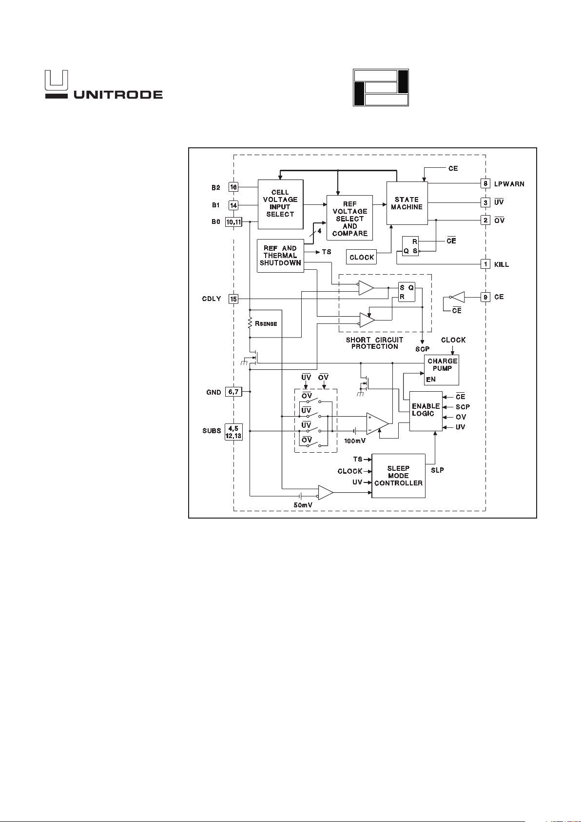
BLOCK DIAGRAM
UDG-95130-2
The UCC3911 is a two-cell lithium-ion battery pack pro
-
tector IC that incorporates an on-chip series FET switch
thus reducing manufacturing costs and increasing reli
-
ability. The IC’s primary function is to protect both lith
-
ium-ion cells in a two-cell battery pack from being either
overcharged or over-discharged. It employs a precision
bandgap voltage reference that is used to detect when
either cell is approaching an overcharged or
over-discharged state. When on board logic detects ei
-
ther condition, the series FET switch opens to protect the
cells.
A negative feedback loop controls the FET switch when
the battery pack is in either the overcharged or
over-discharged state. In the overcharged state the ac
-
tion of the feedback loop is to allow only discharge cur
-
rent to pass through the FET switch. In the
over-discharged state, only charging current is allowed to
flow. The op amp that drives the loop is powered only
when in one of these two states. In the over-discharged
state the chip enters sleep mode until it senses that the
pack is being charged.
The FET switch is driven by a charge pump when the
battery pack is in a normally charged state to achieve the
lowest possible RDS
ON. In this state the negative feed
-
back loop’s op amp is powered down to conserve battery
power. Short circuit protection for the battery pack is pro
-
vided and has a nominal delay of 100µs before tripping.
An external capacitor may be connected between CDLY
and B0 to increase this delay time to allow longer
overcurrent transients.
A chip enable (CE) pin is provided that while held low, in
-
hibits normal operation of the chip to facilitate assembly
of the battery pack.
The UCC3911 is specified for operation over the temper
-
ature range of −20°C to +70°C, the typical operating and
storage temperature range of lithium-ion batteries.
DESCRIPTION
application
INFO
available
2
UCC3911 -1/-2/-3/-4
ELECTRICAL CHARACTERISTICS:
Unless otherwise specified, these specifications apply for –20°C to +70°C for the
UCC3911, all voltages are referenced to B0, V
B2
= 7.2V, T
A
=T
J
.
PARAMETER TEST CONDITIONS MIN TYP MAX UNITS
State Transition Threshold
Normal to Overcharge UCC3911-1 4.15 4.2 4.25 V
Overcharge to Normal 3.6 3.7 3.8 V
Normal to Overcharge UCC3911-2 4.2 4.25 4.3 V
Overcharge to Normal 3.65 3.75 3.85 V
Normal to Overcharge UCC3911-3 4.25 4.3 4.35 V
Overcharge to Normal 3.7 3.8 3.9 V
Normal to Overcharge UCC3911-4 4.3 4.35 4.4 V
Overcharge to Normal 3.75 3.85 3.95 V
Normal to Undercharge 2.42 2.5 2.58 V
Undercharge to Normal 2.90 3.0 3.10 V
B0/GND Switch
V
B0
-V
GND
(Normal) IGND = 2A –320 –160 mV
(Normal) I
GND = –2A 160 320 mV
(Overcharge) I
GND = 1mA –300 –150 mV
(Overcharge) I
GND = 2A –500 –250 mV
(Undercharge) I
GND = –1mA 150 300 mV
(Undercharge) I
GND = –2A 250 500 mV
I
GND (Overcharge) VGND = –5V –5 µA
(Undercharge) V
GND = 5V 0 30 µA
Chip Bias Current
I
B2 Nominal 18 25 µA
I
B2 In Sleep Mode 3.5 µA
I
B1 –1 0 1 µA
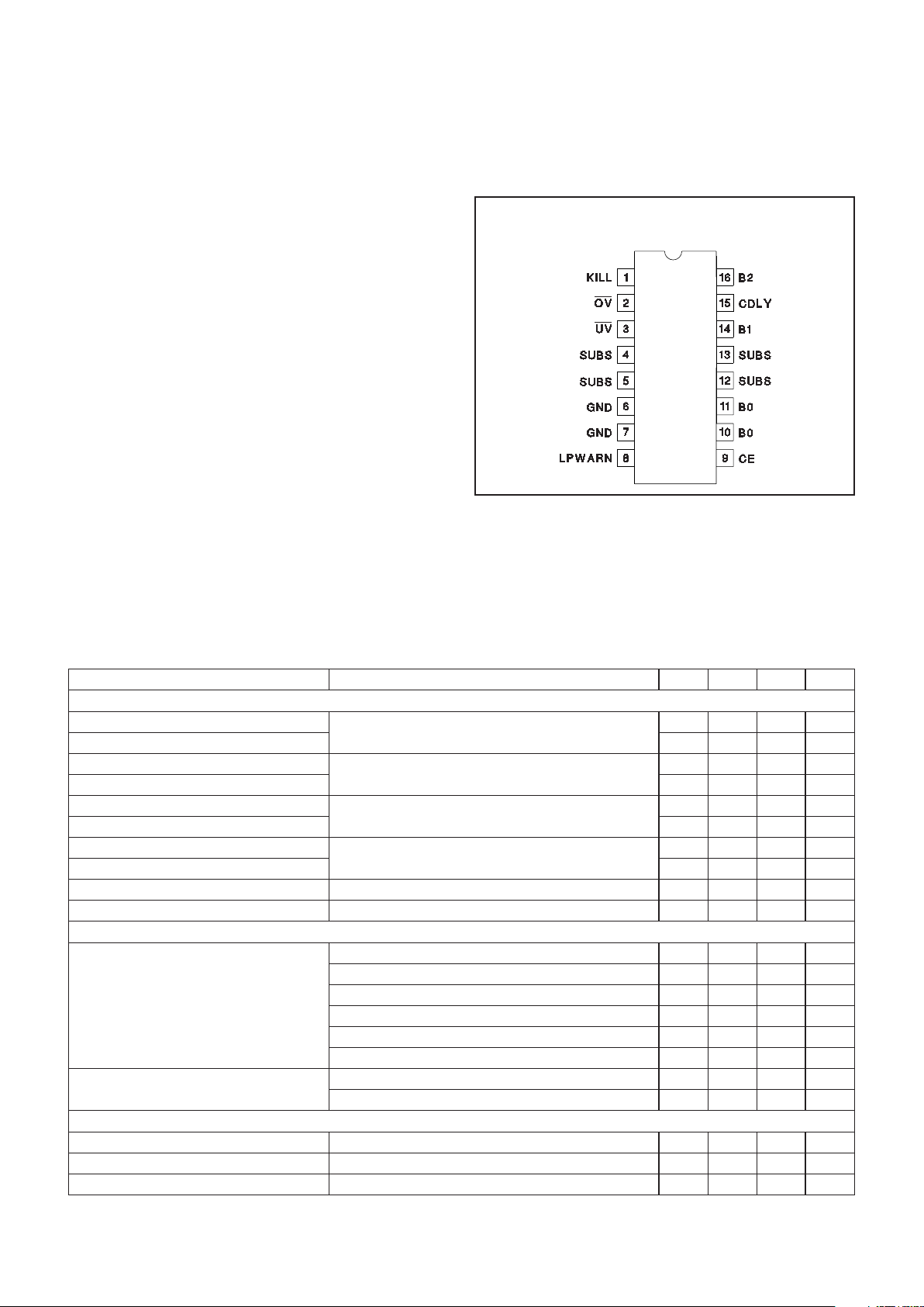
CONNECTION DIAGRAM
SOIC-16 (Top View)
DP Package
ABSOLUTE MAXIMUM RATINGS
Maximum Input Voltage (B2, GND) . . . . . . . . . . . . . . . . . . . 14V
Minimum Input Voltage (B0, GND) . . . . . . . . . . . . . . . . . . −9.0V
Maximum Charge Current (B0, GND) . . . . . . . . . . . . . . . . 3.3A
Minimum Discharge Current (B0, GND) . . . . . . . . . . . . . . . 3.3A
Storage Temperature . . . . . . . . . . . . . . . . . . . −65°C to +150°C
Junction Temperature. . . . . . . . . . . . . . . . . . . –55°C to +150°C
Lead Temperature (Soldering, 10 sec.) . . . . . . . . . . . . . +300°C
Currents are positive into, negative out of the specified terminal.
Consult Packaging Section of Databook for thermal limitations
and considerations of packages.
 Loading...