


TEXAS INSTRUMENTS UCC1809-1, UCC1809-2, UCC2809-1, UCC2809-2, UCC3809-1 Technical data
...application
INFO
available
UCC1809-1/-2 UCC2809-1/-2 UCC3809-1/-2
Economy Primary Side Controller
FEATURES
•User Programmable Soft Start With Active Low Shutdown
•User Programmable Maximum Duty Cycle
•Accessible 5V Reference
•Undervoltage Lockout
•Operation to 1MHz
•0.4A Source/0.8A Sink FET Driver
•Low 100 A Startup Current
PART |
TURN ON |
TURN OFF |
NUMBER |
THRESHOLD |
THRESHOLD |
UCCX809-1 |
10V |
8V |
UCCX809-2 |
15V |
8V |
DESCRIPTION
The UCC3809 family of BCDMOS economy low power integrated circuits contains all the control and drive circuitry required for off-line and isolated DC-to-DC fixed frequency current mode switching power supplies with minimal external parts count. Internally implemented circuits include undervoltage lockout featuring startup current less than 100 A, a user accessible voltage reference, logic to ensure latched operation, a PWM comparator, and a totem pole output stage to sink or source peak current. The output stage, suitable for driving N-Channel MOSFETs, is low in the off state.
Oscillator frequency and maximum duty cycle are programmed with two resistors and a capacitor. The UCC3809 family also features full cycle soft start.
The family has UVLO thresholds and hysteresis levels for off-line and DC-to-DC systems as shown in the table to the left.
The UCC3809 and the UCC2809 are offered in the 8 pin SOIC (D), PDIP (N), TSSOP (PW), and MSOP (P) packages. The small TSSOP and MSOP packages make the device ideal for applications where board space and height are at a premium.
TYPICAL APPLICATION DIAGRAM
|
RSTART |
|
|
|
|
|
|
VIN |
|
|
|
|
|
|
|
|
|
FB |
1V |
– |
|
|
|
|
|
|
1 |
+ |
|
|
|
|
|
|
1V |
|
|
|
REF |
|
|
NOISE |
|
+ |
|
|
|
|
|
|
|
|
|
||
|
|
FILTER |
|
|
5V |
|
|
|
|
+5V |
|
|
8 |
|
|
FEEDBACK |
|
|
– |
|
REF |
|
|
|
|
6 A |
|
|
|
CREF |
|
|
|
SS |
|
|
|
||
|
|
|
2 |
– |
|
|
V |
CURRENT |
SLOPE |
|
|
|
|
|
|
|
0.5V |
+ |
|
|
OUT |
||
|
|
|
|
||||
SENSE |
COMP |
|
|
|
VDD |
||
CSS |
|
|
|
|
|||
|
|
|
|
|
|
||
|
|
|
|
|
– |
7 |
|
|
|
DISABLE |
|
|
+ |
15/8V |
|
|
|
|
|
10/8V |
|
||
|
|
|
|
|
|
||
|
|
|
|
|
|
|
|
|
|
|
|
|
UVLO |
17.5V |
CVDD |
|
|
RT1 |
|
|
PWM |
|
|
|
|
|
3 |
|
LATCH |
|
|
|
|
|
|
|
|
|
|
|
|
|
|
|
R |
|
OUT |
|
|
|
|
CLK |
|
|
|
|
|
|
|
|
|
– |
|
|
|
RT2 |
OSC |
|
Q |
6 |
|
|
|
|
|
S |
|
+ |
|
|
|
|
4 |
|
|
||
|
|
|
|
|
|
GND |
|
|
|
CT |
|
|
|
5 |
VREF |
|
|
|
|
|
|
||
|
|
|
|
|
|
|
|
|
|
|
|
|
|
|
UDG-99036 |
SLUS166B - NOVEMBER 1999 - REVISED NOVEMBER 2004 |
|
|
|||||
ABSOLUTE MAXIMUM RATINGS*
VDD . . . . . . . . . . . . . . . . . . . . . . . . . . . . . . . . . . . . . . . . . . . 19V
IVDD. . . . . . . . . . . . . . . . . . . . . . . . . . . . . . . . . . . . . . . . . . 25mA IOUT (tpw < 1 s and Duty Cycle < 10%) . . . . . . . . –0.4A to 0.8A RT1, RT2, SS . . . . . . . . . . . . . . . . . . . . . . –0.3V to REF + 0.3V
IREF . . . . . . . . . . . . . . . . . . . . . . . . . . . . . . . . . . . . . . . . . –15mA Storage Temperature . . . . . . . . . . . . . . . . . . . –65°C to +150°C
Junction Temperature. . . . . . . . . . . . . . . . . . . –55°C to +150°C Lead Temperature (Soldering, 10 sec.) . . . . . . . . . . . . . +300°C
* Values beyond which damage may occur.
All voltages are with respect to ground unless otherwise stated. Currents are positive into, negative out of the specified terminal. Consult Packaging Section of Databook for thermal limitations and considerations of packages.
UCC1809-1/-2
UCC2809-1/-2
UCC3809-1/-2
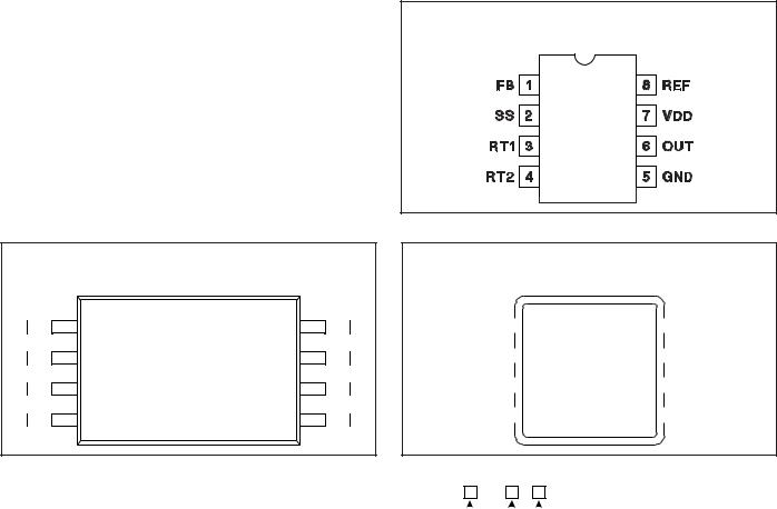
CONNECTION DIAGRAM
SOIC-8, DIL-8 (Top View)
D, N and J Packages
TSSOP-8 (Top View) |
|
|
|
PW Package |
|
|
|
1 |
FB |
REF |
8 |
2 |
SS |
VDD |
7 |
3 |
RT1 |
OUT |
6 |
4 |
RT2 |
GND |
5 |
MSOP-8 (Top View)
P Package
|
1 |
|
FB |
REF |
|
8 |
|
|
|
|
|
|
|
|
|
|
2 |
|
SS |
VDD |
|
7 |
|
|
|
|
|
|
|
|
|
|
3 |
|
RT1 |
OUT |
|
6 |
|
|
|
|
|
GND |
|
|
|
|
4 |
|
RT2 |
|
5 |
|
|
|
|
|
ORDERING INFORMATION |
|||||
|
Temperature Range |
Available Packages |
UCC 809 – |
|||||
UCC1809-X |
–55°C to +125°C |
J |
|
|
|
|
UVLO OPTION |
|
|
|
|
|
|||||
|
|
|
|
|
|
|
||
UCC2809-X |
–40°C to +85°C |
N, D, P, PW |
||||||
|
|
|
|
PACKAGE |
||||
UCC3809-X |
0°C to +70°C |
N, D, P, PW |
|
|
|
|
||
|
|
|
|
|||||
|
|
|
|
|
||||
|
|
|
|
|
|
|
TEMPERATURE RANGE |
|
|
|
|
|
|
|
|
||
ELECTRICAL CHARACTERISTICS: Unless otherwise specified, CVREF = 0.47 F, VDD = 12V. TA = TJ.
PARAMETER |
TEST CONDITIONS |
MIN |
TYP |
MAX |
UNIT |
Supply Section |
|
|
|
|
|
VDD Clamp |
IVDD = 10mA |
16 |
17.5 |
19 |
V |
IVDD |
No Load |
|
600 |
900 |
A |
IVDD Starting |
(Note 1) |
|
110 |
|
A |
IVDD Standby |
UCCx809-1, VDD = Start Threshold - 300mV |
|
110 |
125 |
A |
|
UCCx809-2, VDD = Start Threshold - 300mV |
|
130 |
170 |
A |
Undervoltage Lockout Section |
|
|
|
|
|
Start Threshold (UCCx809-1) |
|
9.4 |
|
10.4 |
V |
UVLO Hysteresis (UCCx809-1) |
|
1.65 |
|
|
V |
Start Threshold (UCCx809-2) |
|
14.0 |
|
15.6 |
V |
UVLO Hysteresis (UCCx809-2) |
|
6.2 |
|
|
V |
Voltage Reference Section |
|
|
|
|
|
Output Voltage |
IREF = 0mA |
4.75 |
5 |
5.25 |
V |
Line Regulation |
VDD = 10V to 15V |
|
2 |
|
mV |
Load Regulation |
IREF = 0mA to 5mA |
|
2 |
|
mV |
Comparator Section |
|
|
|
|
|
IFB |
Output Off |
|
–100 |
|
nA |
Comparator Threshold |
|
0.9 |
0.95 |
1 |
V |
OUT Propagation Delay (No Load) |
VFB = 0.8V to 1.2V at TR = 10ns |
|
50 |
100 |
ns |
2
UCC1809-1/-2
UCC2809-1/-2
UCC3809-1/-2
ELECTRICAL CHARACTERISTICS: Unless otherwise specified, CVREF = 0.47 F, VDD = 12V. TA = TJ.
|
PARAMETER |
TEST CONDITIONS |
MIN |
TYP |
MAX |
UNIT |
Soft Start Section |
|
|
|
|
|
|
ISS |
|
VDD = 16V, VSS = 0V; –40 C to 85 C |
–4.9 |
–7.0 |
–9.1 |
A |
|
|
VDD = 16V, VSS = 0V; –40 C; 85 C |
–4.0 |
–7.0 |
–10.0 |
A |
VSS Low |
VDD = 7.5V, ISS = 200 A |
|
|
0.2 |
V |
|
Shutdown Threshold |
|
0.44 |
0.48 |
0.52 |
V |
|
Oscillator Section |
|
|
|
|
|
|
Frequency |
RT1 = 10k, RT2 = 4.32k, CT = 820pF |
90 |
100 |
110 |
kHz |
|
Frequency Change with Voltage |
VDD = 10V to 15V |
|
0.1 |
|
%/V |
|
CT Peak Voltage |
|
|
3.33 |
|
V |
|
CT |
Valley Voltage |
|
|
1.67 |
|
V |
CT |
Peak to Peak Voltage |
|
1.54 |
1.67 |
1.80 |
V |
Output Section |
|
|
|
|
|
|
Output VSAT Low |
IOUT = 80mA (dc) |
|
0.8 |
1.5 |
V |
|
Output VSAT High |
IOUT = –40mA (dc), VDD – OUT |
|
0.8 |
1.5 |
V |
|
Output Low Voltage During UVLO |
IOUT = 20mA (dc) |
|
|
1.5 |
V |
|
Minimum Duty Cycle |
VFB = 2V |
|
0 |
|
% |
|
Maximum Duty Cycle |
|
|
70 |
|
% |
|
Rise Time |
COUT = 1nF |
|
35 |
|
ns |
|
Fall Time |
COUT = 1nF |
|
18 |
|
ns |
|
Note 1. Ensured by design. Not 100% production tested.
PIN DESCRIPTIONS
FB: This pin is the summing node for current sense feedback, voltage sense feedback (by optocoupler) and slope compensation. Slope compensation is derived from the rising voltage at the timing capacitor and can be buffered with an external small signal NPN transistor. External high frequency filter capacitance applied from this node to GND is discharged by an internal 250 on resistance NMOS FET during PWM off time and offers effective leading edge blanking set by the RC time constant of the feedback resistance from current sense resistor to FB input and the high frequency filter capacitor capacitance at this node to GND.
GND: Reference ground and power ground for all functions.
OUT: This pin is the high current power driver output. A minimum series gate resistor of 3.9 is recommended to limit the gate drive current when operating with high bias voltages.
REF: The internal 5V reference output. This reference is buffered and is available on the REF pin. REF should be bypassed with a 0.47 F ceramic capacitor.
RT1: This pin connects to timing resistor RT1 and controls the positive ramp time of the internal oscillator (Tr = 0.74 (CT + 27pF) RT1). The positive threshold of the internal oscillator is sensed through inactive timing resistor RT2 which connects to pin RT2 and timing capacitor CT.
RT2: This pin connects to timing resistor RT2 and controls the negative ramp time of the internal oscillator (Tf = 0.74 (CT + 27pF) RT2). The negative threshold of the internal oscillator is sensed through inactive timing resistor RT1 which connects to pin RT1 and timing capacitor CT.
SS: This pin serves two functions. The soft start timing capacitor connects to SS and is charged by an internal 6 A current source. Under normal soft start SS is discharged to at least 0.4V and then ramps positive to 1V during which time the output driver is held low. As SS charges from 1V to 2V soft start is implemented by an increasing output duty cycle. If SS is taken below 0.5V, the output driver is inhibited and held low. The user accessible 5V voltage reference also goes low and IVDD < 100 A.
VDD: The power input connection for this device. This pin is shunt regulated at 17.5V which is sufficiently below the voltage rating of the DMOS output driver stage. VDD should be bypassed with a 1 F ceramic capacitor.
3

UCC1809-1/-2
UCC2809-1/-2
UCC3809-1/-2
APPLICATION INFORMATION
OUT |
|
|
|
|
|
|
|
|
|
|
|
|
|
|
|
|
OUT |
|
|
|
|
|
|
|
|
|
|
|
|
|
|
|
|
|
|
|
+V |
|
|
|
|
|
|
|
|
|
|
|
|
C19 |
330 F |
6.3V |
–V |
|
|
|
|
|
|
|
|
|
|
|
|
|
|
|
|
|
|
|
|
|
|
|
|
|
|
|
|
|
|
|
|
|
C18 |
330 F |
6.3V |
|
|
|
|
|
|
|
|
|
|
|
|
|
|
|
|
|
|
|
|
|
|
R17 |
12.1K 1% |
|
|
|
R16 |
12.1K |
1% |
|
|
|
|
C17 |
330 F |
6.3V |
|
|
|
|
|
|
|
|
|
|
|
|
|
|
|
|
|
|
|
|
|
R14 |
750 |
C13 0.1 F |
C14 |
470pF |
U4 |
TL431 |
|
|
|
|
U2 |
|
C16 |
330 F |
6.3V |
|
|
|
|
|
|
|
|
|
|
|
|
|
|
|
|
|
|
|
|
|
R15 |
|
|
|
|
MBR2535CTL |
|
|
|
|
|
|
|
|
|
|
|
|
|
|
|
|
|
|
|
|
|||||||||||
|
|
|
|
|
10K |
|
|
|
|
|
|
|
|
|
|
|
|
|
|
|
|
|
|
|
|
|
|
|
|
|
|
|
|
|
|
|
|
|
|
|
|
|
|
|
|
|
|
|
|
|
|
3 |
|
|
|
|
|
|
|
|
|
|
|
|
|
|
|
|
|
|
|
|
|
|
|
|
|
|
|
|
|
2 |
|
|
|
|
|
|
|
|
|
|
|
|
|
|
|
|
|
|
|
|
|
|
|
|
|
|
|
|
|
|
|
|
|
|
|
|
|
|
|
|
|
|
|
1 |
|
|
|
|
|
|
|
|
|
|
|
|
|
|
|
|
|
|
|
|
|
|
|
|
|
|
|
|
|
R19 |
5.1K |
3W |
|
|
C15 |
0.015 F |
|
|
|
|
|
|
|
|
|
|
|
|
|
|
|
|
|
|
|
|
|
|
|
1 |
|
|
2 |
|
|
|
|
|
|
|
|
|
|
|
|
|
|
|
|
|
|
|
|
|
|
|
|
|
|
|
|
|
|
|
|
|
H11AV1 |
|
|
|
U3 |
|
|
|
|
0.22 F |
|
|
|
T1 |
80 H |
|
5:1 |
Q3 |
|
IRF640 |
|
|
|
|
|
|
R8 |
0.15 |
3W |
|
|
|
|
|
||
|
5 |
|
|
4 |
|
|
C10 |
|
D3 SF24 |
|
|
|
|
|
|
|
|
|
|
|
|
|
|
|
R7 |
15K |
|
|
|
|
||||||
|
|
|
|
|
|
|
|
R9 |
2K |
3W |
|
|
|
|
|
|
|
|
|
|
|
|
R6 |
1K |
|
|
|
|
|
|
|
|
|
|
|
|
|
|
|
|
|
|
|
|
R13 |
1.1K |
|
|
Q2 |
2N2907A |
|
R11 |
680 |
R10 |
10 |
|
|
|
|
|
|
|
D2 |
1N5245 |
|
|
|
||||||
|
|
|
|
|
|
|
|
|
|
|
D4 |
1N5240 |
|
|
R12 |
27K |
|
|
C7 |
0.47 F |
|
|
|
|
|
|
|
|
|
|
|
|
|
|
||
|
|
|
|
|
|
|
|
|
|
|
|
|
|
|
|
|
|
|
|
C9 |
0.1 F |
|
|
|
|
|
|
|
|
|
D1 |
5231B |
|
|
|
|
|
|
|
|
|
|
|
|
|
|
|
|
|
|
|
|
|
UCC3809 |
FBREF |
|
C8 |
1 F |
RT2GND |
|
|
|
|
5.62K |
Q4 C22 2N2222A0.1 F |
C6 |
330pF |
|
3.01K |
|
|||
|
|
|
|
|
|
|
|
|
|
|
|
|
|
|
|
|
|
SSVDD |
|
RT1OUT |
U1 |
|
|
R20 |
|
|
R18 |
|
||||||||
|
|
|
|
|
|
|
|
|
|
|
|
|
|
|
|
|
|
8 |
|
7 |
|
6 |
5 |
|
|
|
|
|
|
|
|
|
|
|
|
|
|
|
|
|
|
|
|
|
|
|
|
|
|
|
|
|
|
|
1 |
|
2 |
|
3 |
4 |
|
|
|
|
|
|
|
|
|
|
|
|
|
|
|
|
|
|
|
|
|
|
|
|
|
R5 |
470 |
|
|
|
|
|
|
|
|
|
|
|
|
R4 |
6.19K |
|
|
|
|
|
1nF |
|
|
|
|
|
|
|
|
|
|
|
|
C3 |
|
1 F |
|
|
|
PGND1 |
|
TP1 |
|
|
|
|
|
|
|
R3 |
12.1K |
|
|
|
|
C4 |
0.01 F |
C5 |
|
|
|
|
|
|
|
|
|
|
|
|
|
|
|
|
|
|
|
|
|
|
|
|
|
|
|
|
|
|
|
Q1 |
2N2222A |
|
|
|
1.1K |
|
|
|
|
|
|
|
|
|
|
|
|
|
|
|
|
|
C2 |
150 F |
|
|
|
|
|
|
|
|
|
R1 |
5.1k |
|
|
|
|
R2 |
|
|
PGND1 |
||
|
|
|
|
|
|
|
|
|
|
|
|
|
|
|
|
|
F |
|
|
|
|
|
|
|
|
|
|
|
|
|
|
|
|
|
|
|
|
|
|
|
|
|
|
|
+VIN |
|
|
|
|
|
|
|
C1 |
150 |
|
|
|
|
|
|
|
ON/OFF |
|
|
|
|
|
|
|
|
|
–VIN |
UDG-99179 |
|
|
|
|
|
|
|
|
|
|
|
|
|
|
|
|
|
|
|
|
|
|
|
|
|
|
|
|
|
|
|
|
|
|
|
|
|
Figure 1. Isolated 50W flyback converter utilizing the UCC3809. The switching frequency is 70kHz, Vin = -32V to -72V, Vout = +5V, Iout = 0A to 10A
4
|
|
UCC1809-1/-2 |
|
|
|
UCC2809-1/-2 |
|
|
|
UCC3809-1/-2 |
|
APPLICATION INFORMATION (cont.) |
|
|
|
The Typical Application Diagram shows an isolated |
reference) sensed through RT1. The R input to the oscil- |
||
flyback converter utilizing the UCC3809. Note that the |
lator latch, R(OSC), is also level sensitive and resets the |
||
capacitors CREF and CVDD are local decoupling capaci- |
CLK signal low when CT crosses the 1.67V threshold, |
||
tors for the reference and IC input voltage, respectively. |
turning off Q2 and turning on Q1, initiating another charg- |
||
Both capacitors should be low ESR and ESL ceramic, |
ing cycle. |
|
|
placed as close to the IC pins as possible, and returned |
Figure 3 shows the waveforms associated with the oscil- |
||
directly to the ground pin of the chip for best stability. |
|||
lator latch and the PWM latch (shown in the Typical Ap- |
|||
REF provides the internal bias to many of the IC func- |
|||
plication Diagram). A high CLK signal not only initiates a |
|||
tions and CREF should be at least 0.47 F to prevent REF |
|||
discharge cycle for CT, it also turns on the internal NMOS |
|||
from drooping. |
FET on the FB pin causing any external capacitance |
||
|
|||
FB Pin |
used for leading edge blanking connected to this pin to |
||
The basic premise of the UCC3809 is that the voltage |
be discharged to ground. By discharging any external |
||
capacitor completely to ground |
during the external |
||
sense feedback signal originates from an optocoupler |
|||
switch’s off-time, the noise immunity of the converter is |
|||
that is modulated by an external error amplifier located |
|||
enhanced allowing the user to design in smaller RC com- |
|||
on the secondary side. This signal is summed with the |
|||
ponents for leading edge blanking. |
A high CLK signal |
||
current sense signal and any slope compensation at the |
|||
also sets the level sensitive S input of the PWM latch, |
|||
FB pin and compared to a 1V threshold, as shown in the |
|||
S(PWM), high, resulting in a high output, Q(PWM), as |
|||
Typical Application Diagram. Crossing this 1V threshold |
|||
shown in Figure 3. This Q(PWM) signal will remain high |
|||
resets the PWM latch and modulates the output driver |
|||
until a reset signal, R(PWM) is received. A high R(PWM) |
|||
on-time much like the current sense comparator used in |
|||
signal results from the FB signal crossing the 1V thresh- |
|||
the UC3842. In the absence of a FB signal, the output |
|||
old, or during soft start or if the SS pin is disabled. |
|||
will follow the programmed maximum on-time of the os- |
|||
|
|
||
cillator. |
Assuming the UVLO threshold is satisfied, the OUT sig- |
||
When adding slope compensation, it is important to use |
nal of the IC will be high as long as Q(PWM) is high and |
||
|
|
||
a small capacitor to AC couple the oscillator waveform
S(PWM), also referred to as CLK, is low. The OUT sig-
before summing this signal into the FB pin. By correctly
nal will be dominated by the FB signal as long as the FB
selecting the emitter resistor of the optocoupler, the volt-
signal trips the 1V threshold while CLK is low. If the FB
age sense signal can force the FB node to exceed the
signal does not cross the 1V threshold while CLK is low,
1V threshold when the output that is being compared ex-
the OUT signal will be dominated by the maximum duty
ceeds a desired level. Doing so drives the UCC3809 to
cycle programmed by the user. Figure 3 illustrates the
zero percent duty cycle.
various waveforms for a design set up for a maximum duty cycle of 70%.
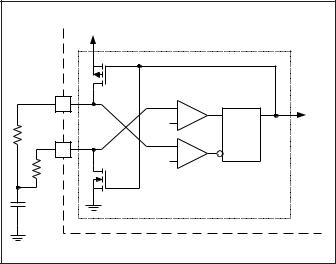
Oscillator
The following equation sets the oscillator frequency:
FOS C =[0.74 • (CT + 27pF )• (RT1+RT 2)]−1
DMAX = 0.74 • RT1• (CT + 27pF )• FOS C
Referring to Figure 2 and the waveforms in Figure 3,
when Q1is on, CT charges via the RDS(on) of Q1 and RT1. During this charging process, the voltage of CT is
sensed through RT2. The S input of the oscillator latch, S(OSC), is level sensitive, so crossing the upper threshold (set at 2/3 VREF or 3.33V for a typical 5.0V reference) sets the Q output (CLK signal) of the oscillator latch high. A high CLK signal results in turning off Q1 and turning on Q2. CT now discharges through RT2 and the
RDS(on) of Q2. CT discharges from 3.33V to the lower threshold (set at 1/3 VREF or 1.67V for a typical 5.0V
VREF |
|
|
|
|
Q1 |
|
|
|
|
3 |
+ |
|
|
|
|
|
|
CLK |
|
3.33V |
– |
S |
Q |
|
|
|
|
||
RT1 |
|
|
|
|
4 |
+ |
R |
|
|
|
|
|
||
1.67V |
– |
|
|
|
|
|
|
||
RT2 |
|
OSCILLATOR |
|
|
Q2 |
|
LATCH |
|
|
|
|
|
||
CT |
OSC |
|
|
|
|
|
|
|
UDG-97195 |
Figure 2. UCC3809 oscillator.
5

UCC1809-1/-2
UCC2809-1/-2
UCC3809-1/-2
APPLICATION INFORMATION (cont.)
CT |
CT |
|
|
CHARGING |
DISCHARGING |
|
|
3.33V |
|
|
|
1.67V |
|
|
|
CT |
|
|
|
S(OSC) |
|
|
|
R(OSC) |
|
|
|
Q(OSC)=CLK |
|
|
|
=S(PWM) |
|
|
|
1V |
|
|
|
FB |
|
|
|
R(PWM) |
|
|
|
Q(PWM) |
|
|
|
|
|
70% |
30% |
|
|
ON |
OFF |
OUT |
|
|
|
FB SIGNAL DOMINANT |
MAX. DUTY CYCLE DOMINANT |
||
|
|
|
UDG-99037 |
Figure 3. Waveforms associated with the oscillator latch and the PWM latch.
The recommended value for CT is 1nF for frequencies in the 100 kHz or less range and smaller CT for higher frequencies. The minimum recommended values of RT1 and RT2 are 10kΩ and 4.32kΩ, respectively. Using these values maintains a ratio of at least 20:1 between the
RDS(on) of the internal FETs and the external timing resistors, resulting in minimal change in frequency over tem-
perature. Because of the oscillator's susceptibility to capacitive coupling, examine the oscillator frequency by looking at the common RT1-RT2-CT node on the circuit board as opposed to looking at pins 3 and 4 directly. For good noise immunity, RT1 and RT2 should be placed as close to pins 3 and 4 of the IC as possible. CT should be returned directly to the ground pin of the IC with minimal stray inductance and capacitance.
|
1000 |
|
|
[kHz] |
|
|
|
FREQUENCY |
100 |
|
|
|
|
|
|
|
10 |
|
|
|
100 |
1000 |
10000 |
|
|
CT [pF] |
|
Figure 4. Oscillator frequency vs. CT (RT1 = 10k, |
|
||
RT2 = 4.32k) |
|
|
|
6
 Loading...