


Texas Instruments UC3849QTR, UC3849Q, UC3849N, UC3849DWTR, UC3849DW Datasheet
...
UC1849
UC2849
UC3849
Secondary Side Average Current Mode Controller
FEATURES
•Practical Secondary Side Control of Isolated Power Supplies
•1MHz Operation
•Differential AC Switching Current Sensing
•Accurate Programmable Maximum Duty Cycle
•Multiple Chips Can be Synchronized to Fastest Oscillator
•Wide Gain Bandwidth Product (70MHz, Acl>10) Current Error and Current Sense Amplifiers
•Up to Ten Devices Can Easily Share a Common Load
BLOCK DIAGRAM
DESCRIPTION
The UC1849 family of average current mode controllers accurately accomplishes secondary side average current mode control. The secondary side output voltage is regulated by sensing the output voltage and differentially sensing the AC switching current. The sensed output voltage drives a voltage error amplifier. The AC switching current, monitored by a current sense resistor, drives a high bandwidth, low offset current sense amplifier. The outputs of the voltage error amplifier and current sense amplifier differentially drive a high bandwidth, integrating current error amplifier. The sawtooth waveform at the current error amplifier output is the amplified and inverted inductor current sensed through the resistor. This inductor current downslope compared to the PWM ramp achieves slope compensation, which gives an accurate and inherent fast transient response to changes in load.
The UC1849 features load share, oscillator synchronization, undervoltage lockout, and programmable output control. Multiple chip operation can be achieved by connecting up to ten UC1849 chips in parallel. The SHARE bus and CLKSYN bus provide load sharing and synchronization to the fastest oscillator respectively. The UC1849 is an ideal controller to achieve high power, secondary side average current mode control.
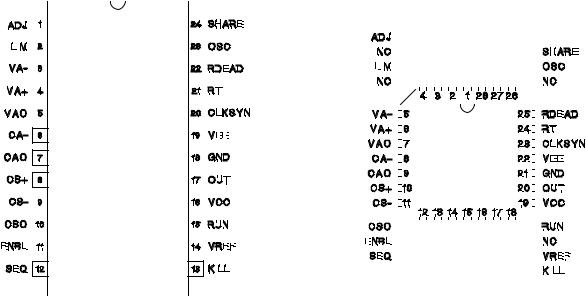
Pin numbers refer to 24-pin packages.
UDG-94110
7/95
ABSOLUTE MAXIMUM RATINGS
Supply Voltage (VCC) . . . . . . . . . . . . . . . . . . . . . . |
. . . . . . .20V |
||||
Output Current Source or Sink . . . . . . . . . . . . . . . . |
. . . . . .0.3A |
||||
Analog Input Voltages . . . . . . . . . . . . . . . . . . . . . . . |
−0.3V to 7V |
||||
ILIM, |
KILL, |
SEQ, |
ENBL, |
. . . . . . . . . . . . . . . .RUN |
−0.3V to 7 V |
CLKSYN Current Source . . . . . . . . . . . . . . . . . . . . |
. . . . .12mA |
||||
RUN Current Sink . . . . . . . . . . . . . . . . . . . . . . . . . . |
. . . . .15mA |
||||
SEQ Current Sink . . . . . . . . . . . . . . . . . . . . . . . . . . |
. . . . .20mA |
||||
RDEAD Current Sink . . . . . . . . . . . . . . . . . . . . . . . |
. . . . .20mA |
||||
Share Bus Voltage (voltage with respect to GND) . . .0V to 6.2V
ADJ Voltage (voltage with respect to GND) . . |
. . . .0.9V to 6.3V |
VEE (voltage with respect to GND) . . . . . . . . |
. . . . . . . . .−1.5V |
Storage Temperature . . . . . . . . . . . . . . . . . . . |
−65°C to +150°C |
UC1849
UC2849
UC3849
Junction Temperature . . . . . . . . . . . . . . . . . . .−65°C to +150°C Lead Temperature (Soldering, 10 sec.) . . . . . . . . . . . . .+300°C
All voltages with respect to VEE except where noted; all currents are positive into, negative out of the specified terminal.
Consult Packaging Section of Databook for thermal limitations and considerations of packages.
RECOMMENDED OPERATING CONDITIONS
Input Voltage . . . . . . . . . . . . . . . . . . . . . . . . . . . . . |
. . .8V to20V |
Sink/Source Output Current . . . . . . . . . . . . . . . . . . |
. . . .250mA |
Timing Resistor (RT) . . . . . . . . . . . . . . . . . . . . . . . . |
.1k to 200k |
Timing Capacitor (CT) . . . . . . . . . . . . . . . . . . . . . . |
75pF to 2nF |
CONNECTION DIAGRAMS
DIL-24, SOIC-24,TSSOP-24 (Top View) |
|
|
|
|
|
|
|
|
|
|
|
|
|
|
|
|
PLCC-28 (Top View) |
|
|
|
|
|
|
|
|
|
|
|
|
|
|
|
|
|
|
|
|
|
|
|
|
|
|
|||||||||||||||||||||||||||||||||||||||||||||||||||||||||||||||||||||||||||||||||||||
J or N, DW, PW Packages |
|
|
|
|
|
|
|
|
|
|
|
|
|
|
|
|
Q Package |
|
|
|
|
|
|
|
|
|
|
|
|
|
|
|
|
|
|
|
|
|
|
|
|
|
|
|||||||||||||||||||||||||||||||||||||||||||||||||||||||||||||||||||||||||||||||||||||
|
|
|
|
|
|
|
|
|
|
|
|
|
|
|
|
|
|
|
|
|
|
|
|
|
|
|
|
|
|
|
|
|
|
|
|
|
|
|
|
|
|
|
|
|
|
|
|
|
|
|
|
|
|
|
|
|
|
|
|
|
|
|
|
|
|
|
|
|
|
|
|
|
|
|
|
|
|
|
|
|
|
|
|
|
|
|
|
|
|
|
|
|
|
|
|
|
|
|
|
|
|
|
|
|
|
|
|
|
|
|
|
|
|
|
|
|
|
|
|
|
|
|
|
|
|
|
|
|
|
|
|
|
|
|
|
|
|
|
|
|
|
|
|
|
|
|
|
|
|
|
|
|
|
|
|
|
|
|
|
|
|
|
|
|
|
|
|
|
|
|
|
|
|
|
|
|
|
|
|
|
|
|
|
|
|
|
|
|
|
|
|
|
|
|
|
|
|
|
|
|
|
|
|
|
|
|
|
|
|
|
|
|
|
|
|
|
|
|
|
|
|
|
|
|
|
|
|
|
|
|
|
|
|
|
|
|
|
|
|
|
|
|
|
|
|
|
|
|
|
|
|
|
|
|
|
|
|
|
|
|
|
|
|
|
|
|
|
|
|
|
|
|
|
|
|
|
|
|
|
|
|
|
|
|
|
|
|
|
|
|
|
|
|
|
|
|
|
|
|
|
|
|
|
|
|
|
|
|
|
|
|
|
|
|
|
|
|
|
|
|
|
|
|
|
|
|
|
|
|
|
|
|
|
|
|
|
|
|
|
|
|
|
|
|
|
|
|
|
|
|
|
|
|
|
|
|
|
|
|
|
|
|
|
|
|
|
|
|
|
|
|
|
|
|
|
|
|
|
|
|
|
|
|
|
|
|
|
|
|
|
|
|
|
|
|
|
|
|
|
|
|
|
|
|
|
|
|
|
|
|
|
|
|
|
|
|
|
|
|
|
|
|
|
|
|
|
|
|
|
|
|
|
|
|
|
|
|
|
|
|
|
|
|
|
|
|
|
|
|
|
|
|
|
|
|
|
|
|
|
|
|
|
|
|
|
|
|
|
|
|
|
|
|
|
|
|
|
|
|
|
|
|
|
|
|
|
|
|
|
|
|
|
|
|
|
|
|
|
|
|
|
|
|
|
|
|
|
|
|
|
|
|
|
|
|
|
|
|
|
|
|
|
|
|
|
|
|
|
|
|
|
|
|
|
|
|
|
|
|
|
|
|
|
|
|
|
|
|
|
|
|
|
|
|
|
|
|
|
|
|
|
|
|
|
|
|
|
|
|
|
|
|
|
|
|
|
|
|
|
|
|
|
|
|
|
|
|
|
|
|
|
|
|
|
|
|
|
|
|
|
|
|
|
|
|
|
|
|
|
|
|
|
|
|
|
|
|
|
|
|
|
|
|
|
|
|
|
|
|
|
|
|
|
|
|
|
|
|
|
|
|
|
|
|
|
|
|
|
|
|
|
|
|
|
|
|
|
|
|
|
|
|
|
|
|
|
|
|
|
|
|
|
|
|
|
|
|
|
|
|
|
|
|
|
|
|
|
|
|
|
|
|
|
|
|
|
|
|
|
|
|
|
|
|
|
|
|
|
|
|
|
|
|
|
|
|
|
|
|
|
|
|
|
|
|
|
|
|
|
|
|
|
|
|
|
|
|
|
|
|
|
|
|
|
|
|
|
|
|
|
|
|
|
|
|
|
|
|
|
|
|
|
|
|
|
|
|
|
|
|
|
|
|
|
|
|
|
|
|
|
|
|
|
|
|
|
|
|
|
|
|
|
|
|
|
|
|
|
|
|
|
|
|
|
|
|
|
|
|
|
|
|
|
|
|
|
|
|
|
|
|
|
|
|
|
|
|
|
|
|
|
|
|
|
|
|
|
|
|
|
|
|
|
|
|
|
|
|
|
|
|
|
|
|
|
|
|
|
|
|
|
|
|
|
|
|
|
|
|
|
|
|
|
|
|
|
|
|
|
|
|
|
|
|
|
|
|
|
|
|
|
|
|
|
|
|
|
|
|
|
|
|
|
|
|
|
|
|
|
|
|
|
|
|
|
|
|
|
|
|
|
|
|
|
|
|
|
|
|
|
|
|
|
|
|
|
|
|
|
|
|
|
|
|
|
|
|
|
|
|
|
|
|
|
|
|
|
|
|
|
|
|
|
|
|
|
|
|
|
|
|
|
|
|
|
|
|
|
|
|
|
|
|
|
|
|
|
|
|
|
|
|
|
|
|
|
|
|
|
|
|
|
|
|
|
|
|
|
|
|
|
|
|
|
|
|
|
|
|
|
|
|
|
|
|
|
|
|
|
|
|
|
|
|
|
|
|
|
|
|
|
|
|
|
|
|
|
|
|
|
|
|
|
|
|
|
|
|
|
|
|
|
|
|
|
|
|
|
|
|
|
|
|
|
|
|
|
|
|
|
|
|
|
|
|
|
|
|
|
|
|
|
|
|
|
|
|
|
|
|
|
|
|
|
|
|
|
|
|
|
|
|
|
|
|
|
|
|
|
|
|
|
|
|
|
|
|
|
|
|
|
|
|
|
|
|
|
|
|
|
|
|
|
|
|
|
|
|
|
|
|
|
|
|
|
|
|
|
|
|
ELECTRICAL CHARACTERISTICS Unless otherwise stated these specifications apply for TA = −55°C to +125°C for UC1849; −40°C to +85°C for UC2849; and 0°C to +70°C for UC3849; VCC = 12V, VEE = GND, Output no load, CT = 345pF, RT = 4530Ω, RDEAD = 511Ω, RCLKSYN = 1k, TA = TJ.
PARAMETER |
TEST CONDITIONS |
MIN |
TYP |
MAX |
UNITS |
Current Sense Amplifier |
|
|
|
|
|
Ib |
|
|
0.5 |
3 |
μA |
Vio |
TA = +25°C |
|
|
3 |
mV |
|
|
|
|
|
|
|
Over Temperature |
|
|
5 |
mV |
Avo |
|
60 |
90 |
|
dB |
|
|
|
|
|
|
GBW (Note 2) |
Acl = 1, RIN = 1k, CC = 15pF, f = 200kHz (Note 1) |
4.5 |
7 |
|
MHz |
Vol |
Io = 1mA, Voltage above VEE |
|
0.5 |
|
V |
Voh |
Io = 0mA |
|
3.8 |
|
V |
|
Io = −1mA |
|
3.5 |
|
V |
CMRR |
−0.2 < Vcm < 8V |
|
80 |
|
dB |
|
|
|
|
|
|
PSRR |
10V < VCC < 20V |
|
80 |
|
dB |
Current Error Amplifier |
|
|
|
|
|
Ib |
|
|
0.5 |
3 |
μA |
Vio |
|
|
3 |
20 |
mV |
2
UC1849
UC2849
UC3849
ELECTRICAL CHARACTERISTICS Unless otherwise stated these specifications apply for TA = −55°C to +125°C for UC1849; −40°C to +85°C for UC2849; and 0°C to +70°C for UC3849; VCC = 12V, VEE = GND, Output no load, CT = 345pF, RT = 4530Ω, RDEAD = 511Ω, RCLKSYN = 1k, TA = TJ.
PARAMETER |
TEST CONDITION |
MIN |
TYP |
MAX |
UNITS |
Current Error Amplifier (cont.) |
|
|
|
|
|
Avo |
|
60 |
90 |
|
dB |
GBW (Note 2) |
Acl = 1, RIN = 1k, CC=15pF, f=200kHz (Note 1) |
4.5 |
7 |
|
MHz |
|
|
|
|
|
|
Vol |
IO = 1mA, Voltage above VEE |
|
0.5 |
|
V |
Voh |
IO = 0mA |
|
3.8 |
|
V |
|
IO = −1mA |
|
3.5 |
|
V |
|
|
|
|
|
|
CMRR |
−0.2 < Vcm < 8V |
|
80 |
|
dB |
PSRR |
10V < VCC < 20V |
|
80 |
|
dB |
Voltage Error Amplifier |
|
|
|
|
|
Ib |
|
|
0.5 |
3 |
μA |
|
|
|
|
|
|
Vio |
|
|
2 |
5 |
mV |
Avo |
|
60 |
90 |
|
dB |
|
|
|
|
|
|
GBW (Note 2) |
f = 200kHz |
4.5 |
7 |
|
MHz |
Vol |
IO = 175μA, Volts above VEE |
|
0.3 |
0.6 |
V |
Voh |
ILIM > 3V |
2.85 |
3 |
3.15 |
V |
Voh - ILIM |
Tested ILIM = 0.5V, 1.0V, 2.0V |
−100 |
|
100 |
mV |
CMRR |
−0.2 < Vcm < 8V |
|
80 |
|
dB |
|
|
|
|
|
|
PSRR |
10V < VCC < 20V |
|
80 |
|
dB |
2X Amplifier and Share Amplifier |
|
|
|
|
|
V offset (b; y = mx + b) |
|
|
|
20 |
mV |
GAIN (m; y = mx + b) |
Slope with AVOUT = 1V and 2V |
1.98 |
|
2.02 |
V |
|
|
|
|
|
|
GBW (Note 2) |
|
|
100 |
|
kHZ |
RSHARE |
VCC = 0, VSHARE/ISHARE |
|
200 |
|
k |
Total Offset |
Negative supply is VEE, GND Open, VAO = GND |
−75 |
0 |
75 |
mV |
Vol |
VAO = Voltage Amplifier Vol, Volts above VEE |
0.2 |
0.45 |
0.6 |
V |
Voh |
IO = 0mA, ILIM = 3V, VAO = Voltage Amp Voh |
5.7 |
6 |
6.3 |
V |
|
IO = −1mA, ILIM = 3V, VAO = Voltage Amp Voh |
5.7 |
6 |
6.3 |
V |
Adjust Amplifier |
|
|
|
|
|
Vio |
|
40 |
60 |
80 |
mV |
gm |
IOUT= −10μA to 10μA, VOUT = 3.5V, CADJ = 1μF |
|
−1 |
|
mS |
|
|
|
|
|
|
Vol |
IOUT = 0 |
0.9 |
1 |
1.1 |
V |
|
IOUT = 50μA |
0.85 |
1 |
1.15 |
V |
|
|
|
|
|
|
Voh |
IOUT = 0, VSHARE = 6.5V |
5.7 |
6 |
6.3 |
V |
|
IOUT = −50μA, VSHARE = 6.5V |
5.7 |
6 |
6.3 |
V |
Oscillator |
|
|
|
|
|
Frequency |
|
450 |
500 |
550 |
kHz |
|
|
|
|
|
|
Max Duty Cycle |
|
80 |
85 |
90 |
% |
OSC Ramp Amplitude |
|
2 |
2.5 |
2.8 |
V |
Clock Driver/SYNC (CLKSYN) |
|
|
|
|
|
Vol |
|
|
0.02 |
0.2 |
V |
Voh |
|
|
3.6 |
|
V |
|
|
|
|
|
|
|
RCLKSYN = 200Ω |
|
3.2 |
|
V |
ISOURCE |
|
|
25 |
|
mA |
|
|
|
|
|
|
RCLKSYN |
VCC = 0, VCLKSYN/ICLKSYN |
|
10 |
|
k |
VTH |
|
|
1.5 |
|
V |
|
|
|
|
|
|
3
UC1849
UC2849
UC3849
ELECTRICAL CHARACTERISTICS (cont)Unless otherwise stated these specifications apply for TA = −55°C to +125°C for UC1849; −40°C to +85°C for UC2849; and 0°C to +70°C for UC3849; VCC = 12V, VEE = GND, Output no load, CT = 345pF, RT = 4530Ω, RDEAD = 511Ω, RCLKSYN = 1k, TA = TJ.
PARAMETER |
TEST CONDITION |
MIN |
TYP |
MAX |
UNITS |
VREF Comparator |
|
|
|
|
|
Turn-on threshold |
|
|
4.65 |
|
V |
Hysteresis |
|
|
0.4 |
|
V |
VCC Comparator |
|
|
|
|
|
Turn-on Threshold |
|
7.9 |
8.3 |
8.7 |
V |
Hysteresis |
|
|
0.4 |
|
V |
KILL Comparator |
|
|
|
|
|
Voltage Threshold |
|
|
3 |
|
V |
Sequence Comparator |
|
|
|
|
|
Voltage Threshold |
|
|
2.5 |
|
V |
SEQ SAT |
IO = 10mA |
|
0.25 |
|
V |
Enable Comparator |
|
|
|
|
|
Voltage Threshold |
|
|
2.5 |
|
V |
|
|
|
|
|
|
RUN SAT |
IO = 10mA |
|
0.25 |
|
V |
Reference |
|
|
|
|
|
VREF |
TA = 25°C |
4.95 |
5 |
5.05 |
V |
VREF |
VCC = 15V |
4.9 |
|
5.1 |
V |
Line Regulation |
10 < VCC < 20 |
|
3 |
15 |
mV |
|
|
|
|
|
|
Load Regulation |
0 < Io < 10mA |
|
3 |
15 |
mV |
Short Circuit I |
VREF = 0V |
30 |
60 |
90 |
mA |
Output Stage |
|
|
|
|
|
Rise Time |
CL = 100pF |
|
10 |
20 |
ns |
|
|
|
|
|
|
Fall Time |
CL = 100pF |
|
10 |
20 |
ns |
Voh |
VCC > 11V, IO = −10mA |
8.0 |
8.4 |
8.8 |
V |
|
|
|
|
|
|
|
IO = −200mA |
7.8 |
|
|
V |
Vol |
IO = 200mA |
|
|
3.0 |
V |
|
IO = 10mA |
|
|
0.5 |
V |
Virtual Ground |
|
|
|
|
|
VGND-VEE |
VEE is externally supplied, GND is floating |
0.2 |
0.75 |
|
V |
|
and used as Signal GND. |
|
|
|
|
Icc |
|
|
|
|
|
Icc (run) |
|
|
21 |
30 |
mA |
|
|
|
|
|
|
Note 1: If a closed loop gain greater than 1 is used, the possible GBW will increase by a factor of ACL + 10; where ACL is the closed loop gain.
Note 2: Guaranteed by design. Not 100% tested in production.
Note 3: Unless otherwise specified all voltages are with respect to GND. Currents are positive into, negative out of the specified terminal.
PIN DESCRIPTIONS
ADJ: The output of the transconductance (gm = −1mS) amplifier adjusts the control voltage to maintain equal current sharing. The chip sensing the highest output current will have its output clamped to 1V. A resistor divider between VREF and ADJ drives the control voltage (VA+) for the voltage amplifier. Each slave unit’s ADJ voltage increases (to a maximum of 6V) its control voltage (VA+) until its load current is equal to the master. The 60mV input offset on the gm amplifier guarantees that the unit sensing the highest load current is chosen as the mas-
ter. The 60mV offset guarantees by design to be greater than the inherent offset of the gm amplifier and the buffer amplifier. While the 60mV offset represents an error in current sharing, the gain of the current and 2X amplifiers reduces it to only 30mV. This pin needs a 1μF capacitor to compensate the amplifier.
CA-: The inverting input to the current error amplifier. This amplifier needs a capacitor between CAand CAO to set its dominant pole.
4
 Loading...