


Texas Instruments UC3901QTR, UC3901Q, UC3901N, UC3901J, UC3901DWTR Datasheet
...
UC1901
UC2901
UC3901
Isolated Feedback Generator
FEATURES
∙An Amplitude-Modulation System for Transformer Coupling an Isolated Feedback Error Signal
∙Low-Cost Alternative to Optical Couplers
∙Internal 1% Reference and Error Amplifier
∙Internal Carrier Oscillator Usable to 5MHz
∙Modulator Synchronizable to an External Clock
∙Loop Status Monitor
UC1901 SIMPLIFIED SCHEMATIC
DESCRIPTION
The UC1901 family is designed to solve many of the problems associated with closing a feedback control loop across a voltage isolation boundary. As a stable and reliable alternative to an optical coupler, these devices feature an amplitude modulation system which allows a loop error signal to be coupled with a small RF transformer or capacitor.
The programmable, high-frequency oscillator within the UC1901 series permits the use of smaller, less expensive transformers which can readily be built to meet the isolation requirements of today's line-operated power systems. As an alternative to RF operation, the external clock input to these devices allows synchronization to a system clock or to the switching frequency of a SMPS.
An additional feature is a status monitoring circuit which provides an activelow output when the sensed error voltage is within ±10% of the reference. The DRIVERA output, DRIVERB output, and STATUS output are disabled until the input supply has reached a sufficient level to allow proper operation of the device.
Since these devices can also be used as a DC driver for optical couplers, the benefits of 4.5 to 40V supply operation, a 1% accurate reference, and a high gain general purpose amplifier offer advantages even though an AC system may not be desired.
μ |
μ |
|
μ |
|
UDG-98080 |
11/98 |
|
ABSOLUTE MAXIMUM RATINGS (Note 1)
Input Supply Voltage, VIN . . . . . . . . . . . . . . . . . . . . . . . . . . 40V Reference Output Current . . . . . . . . . . . . . . . . . . . . . . . –10mA Driver Output Currents . . . . . . . . . . . . . . . . . . . . . . . . . . –35mA Status Indicator Voltage . . . . . . . . . . . . . . . . . . . . . . . . . . . 40V Status Indicator Current . . . . . . . . . . . . . . . . . . . . . . . . . . 20mA Ext. Clock Input . . . . . . . . . . . . . . . . . . . . . . . . . . . . . . . . . . 40V Error Amplifier Inputs . . . . . . . . . . . . . . . . . . . . . –0.5V to +35V Power Dissipation at TA = 25°C. . . . . . . . . . . . . . . . . . 1000mW Power Dissipation at TC = 25°C . . . . . . . . . . . . . . . . . 2000mW Operating Junction Temperature . . . . . . . . . . –55°C to +150°C Storage Temperature . . . . . . . . . . . . . . . . . . . –65°C to +150°C Lead Temperature (Soldering, 10 seconds) . . . . . . . . . . 300°C
Note 1: Voltages are referenced to ground, Pin 7. Currents are positive into, negative out of the specified terminal.
Note 2: Consult Packaging section of Databook for thermal limitations and considerations of package.
UC1901
UC2901
UC3901
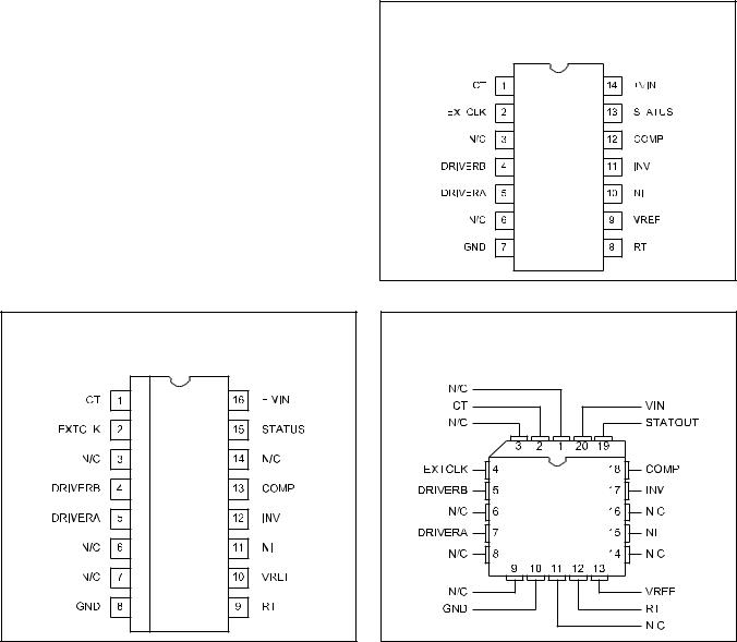
CONNECTION DIAGRAMS
DIL-14, SOIC-14 (TOP VIEW)
J or N Package, D Package
SOIC-16 Wide (TOP VIEW)
DW Package
TEMPERATURE AND PACKAGE SELECTION GUIDE
|
TEMPERATURE |
AVAILABLE |
|
RANGE |
PACKAGES |
UC1901 |
–55°C to +125°C |
J, L |
UC2901 |
–40°C to +85°C |
D, DW, J, N, Q |
UC3901 |
0°C to +70°C |
D, DW, J, N, Q |
PLCC-20, LCC-20 (TOP VIEW)
Q, L Packages
2
UC1901
UC2901
UC3901
ELECTRICAL CHARACTERISTICS Unless otherwise stated, these specifications apply for VIN = 10V, RT = 10kΩ, CT = 820pF, TA = TJ.
PARAMETER |
TEST CONDITIONS |
UC1901/UC2901 |
|
UC3901 |
|
UNITS |
|||
|
|
|
MIN |
TYP |
MAX |
MIN |
TYP |
MAX |
|
Reference Section |
|
|
|
|
|
|
|
|
|
Output Voltage |
TJ = 25°C |
|
1.485 |
1.5 |
1.515 |
1.47 |
1.5 |
1.53 |
V |
|
TMIN ≤ TJ ≤ TMAX |
|
1.470 |
1.5 |
1.530 |
1.455 |
1.5 |
1.545 |
|
Line Regulation |
VIN = 4.5 to 35V |
|
|
2 |
10 |
|
2 |
15 |
mV |
Load Regulation |
IOUT = 0 to 5mA |
|
|
4 |
10 |
|
4 |
15 |
mV |
Short Circuit Current |
TJ = 25°C |
|
|
–35 |
–55 |
|
–35 |
–55 |
mV |
Error Amplifier Section (To Compensation Terminal) |
|
|
|
|
|
|
|
|
|
Input Offset Voltage |
VCM = 1.5V |
|
|
1 |
4 |
|
1 |
8 |
mV |
Input Bias Current |
VCM = 1.5V |
|
|
–1 |
–3 |
|
–1 |
–6 |
μA |
Input Offset Current |
VCM = 1.5V |
|
|
0.1 |
1 |
|
0.1 |
2 |
μA |
Small Signal Open Loop Gain |
|
|
40 |
60 |
|
40 |
60 |
|
dB |
CMRR |
VCM = 0.5 to 7.5V |
|
60 |
80 |
|
60 |
80 |
|
dB |
PSRR |
VIN = 2 to 25V |
|
80 |
100 |
|
80 |
100 |
|
dB |
Output Swing, VO |
|
|
0.4 |
0.7 |
|
0.4 |
0.7 |
|
V |
Maximum Sink Current |
|
|
90 |
150 |
|
90 |
150 |
|
μA |
Maximum Source Current |
|
|
–2 |
–3 |
|
–2 |
–3 |
|
mA |
Gain Band Width Product |
|
|
|
1 |
|
|
1 |
|
MHz |
Slew Rate |
|
|
|
0.3 |
|
|
0.3 |
|
V/μS |
Modulators/Drivers Section (From Compensation Terminal) |
|
|
|
|
|
|
|
||
Voltage Gain |
|
|
11 |
12 |
13 |
10 |
12 |
14 |
dB |
Output Swing |
|
|
±1.6 |
±2.8 |
|
±1.6 |
±2.8 |
|
V |
Driver Sink Current |
|
|
500 |
700 |
|
500 |
700 |
|
μA |
Driver Source Current |
|
|
–15 |
–35 |
|
–15 |
–35 |
|
mA |
Gain Band Width Product |
|
|
|
25 |
|
|
25 |
|
MHz |
Oscillator Section |
|
|
|
|
|
|
|
|
|
Initial Accuracy |
TJ = 25°C |
|
140 |
150 |
160 |
130 |
150 |
170 |
kHz |
|
TMIN ≤ TJ ≤ TMAX |
|
130 |
|
170 |
120 |
|
180 |
kHz |
Line Sensitivity |
VIN = 5 to 35V |
|
|
.15 |
.35 |
|
.15 |
.60 |
%/V |
Maximum Frequency |
RT = 10k, CT = 10pF |
|
5 |
|
|
5 |
|
MHz |
|
Ext. Clock Low Threshold |
Pin 1 (CT) = VIN |
|
0.5 |
|
|
0.5 |
|
|
V |
Ext. Clock High Threshold |
Pin 1 (CT) = VIN |
|
|
|
1.6 |
|
|
1.6 |
V |
Status Indicator Section |
|
|
|
|
|
|
|
|
|
Input Voltage Window |
@ E/A Inputs, VCM = 1.5V |
±135 |
±150 |
±165 |
±130 |
±150 |
±170 |
mV |
|
Saturation Voltage |
E/A Input = 0V, ISINK = 1.6mA |
|
|
0.45 |
|
|
0.45 |
V |
|
Max. Output Current |
Pin 13 = 3V, E/A |
Input = 0.0V |
8 |
15 |
|
8 |
15 |
|
mA |
Leakage Current |
Pin 13 = 40V, E/A |
Input = 0.2V |
|
.05 |
1 |
|
.05 |
5 |
μA |
Supply Current |
VIN = 35V |
|
|
5 |
8 |
|
5 |
10 |
mA |
UVLO Section |
|
|
|
|
|
|
|
|
|
Drivers Enabled Threshold |
At Input Supply VIN |
|
|
3.9 |
4.5 |
|
3.9 |
4.5 |
V |
Status Output Enabled |
At Input Supply VIN |
|
|
3.9 |
4.5 |
|
3.9 |
4.5 |
V |
Threshold |
|
|
|
|
|
|
|
|
|
Change in Reference Output |
When VIN Reaches UVLO |
|
–2 |
–30 |
|
–2 |
–30 |
mV |
|
|
Threshold |
|
|
|
|
|
|
|
|
3
 Loading...