


Texas Instruments UC3914N, UC3914DWTR, UC3914DW, UC2914DWTR, UC2914J Datasheet
...
UC1914 UC2914 UC3914
5V to 35V Hot Swap Power Manager
FEATURES
•5V to 35V Operation
•Precision Maximum Current Control
•Precision Fault Threshold
•Programmable Average Power Limiting
•Programmable Overcurrent Limit
•Shutdown Control
•Charge Pump for Low RDS(on) High-Side Drive
•Latch Reset Function Available
•Output Drive VGS Clamping
•Fault Output Indication
•18 Pin DIL and SOIC Packages
DESCRIPTION
The UC3914 family of Hot Swap Power Managers provides complete power management, hot swap and fault handling capability. Integrating this part and a few external components, allows a board to be swapped in or out upon failure or system modification without removing power to the hardware, while maintaining the integrity of the powered system. Complementary output drivers and diodes have been integrated for use with external capacitors as a charge pump to ensure sufficient gate drive to the external NMOS transistor for low RDS(on). All control and housekeeping functions are integrated and externally programmable and include the fault current level, maximum output sourcing current, maximum fault time and average power limiting of the external FET. The UC3914 features a duty ratio current limiting technique, which provides peak load capability while limiting the average power dissipation of the external pass transistor during fault conditions. The fault level is fixed at 50mV with respect to VCC to minimize total dropout. The fault current level is set with an external current sense resistor. The maximum allowable sourcing current is programmed by using a resistor divider from VCC to REF to set the voltage on IMAX. The maximum current level, when the output appears as a current source is (VCC – VIMAX)/RSENSE.
(continued)
BLOCK DIAGRAM
UDG-95134-2 |
SLUS425A - AUGUST 1999 |
ABSOLUTE MAXIMUM RATINGS
Input Supply Voltage, VCC . . . . . . . . . . . . . . . . . . . . . . . . . 40V Maximum Forced Voltage
SD. . . . . . . . . . . . . . . . . . . . . . . . . . . . . . . . . . . . . . . . . . 12V IMAX . . . . . . . . . . . . . . . . . . . . . . . . . . . . . . . . . . . . . . . VCC LR . . . . . . . . . . . . . . . . . . . . . . . . . . . . . . . . . . . . . . . . . . 12V
Maximum Current
FAULT . . . . . . . . . . . . . . . . . . . . . . . . . . . . . . . . . . . . . 20mA PLIM . . . . . . . . . . . . . . . . . . . . . . . . . . . . . . . . . . . . . . 10mA Maximum Voltage, FAULT . . . . . . . . . . . . . . . . . . . . . . . . . 40V Reference Output Current . . . . . . . . . . . . . . . Internally Limited Storage Temperature . . . . . . . . . . . . . . . . . . . –65°C to +150°C Junction Temperature. . . . . . . . . . . . . . . . . . . –55°C to +150°C Lead Temperature (Soldering, 10 sec.) . . . . . . . . . . . . . +300°C
Unless otherwise indicated, voltages are referenced to ground. Currents are positive into, negative out of specified terminal. Consult Packaging Section of Databook for thermal limitations and considerations of package.
UC1914
UC2914
UC3914
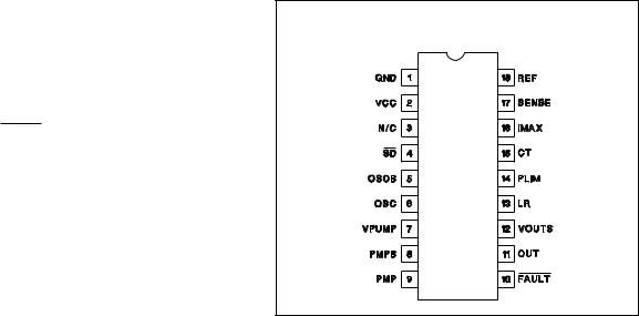
CONNECTION DIAGRAM
DIL-18, SOIC-18 (Top View)
N or J Package, DW Package
DESCRIPTION (cont.)
When the output current is less than the fault level, the external output transistor remains switched on. When the output current exceeds the fault level, but is less than the maximum sourcing level programmed by IMAX, the output remains switched on, and the fault timer starts to charge CT, a timing capacitor. Once CT charges to 2.5V, the output device is turned off and CT is slowly discharged. Once CT is discharged to 0.5V, the IC performs a retry and the output transistor is switched on again. The UC3914 offers two distinct reset modes. In one
mode with LR left floating or held low, the IC will repeatedly try to reset itself if a fault occurs as described above. In the second mode with LR held high, once a fault occurs, the output is latched off until either LR is toggled low, the part is shutdown then re-enabled using SD, or the power to the part is turned off and then on again.
This part is offered in both 18 pin DW Wide-Body (SOIC) and Dual-In-Line (DIL) packages.
ELECTRICAL CHARACTERISTICS: Unless otherwise specified, TA = 0°C to 70°C for the UC3914, –40°C to 85°C for
the UC2914, and –55°C to 125°C for the UC1914. VCC = 12V, VPUMP = VPUMP(max), SD = 5V, CP1 = CP2 = CPUMP = 0.01 F. TA = TJ.
PARAMETER |
|
|
TEST CONDITIONS |
MIN |
TYP |
MAX |
UNITS |
VCC Section |
|
|
|
|
|
|
|
ICC |
|
(Note 2) |
|
8 |
15 |
mA |
|
|
|
VCC = 35V, (Note 2) |
|
12 |
20 |
mA |
|
|
|
|
|
|
|
|
A |
Shutdown ICC |
|
SD = 0V |
|
500 |
900 |
||
UVLO |
|
Turn on threshold |
|
4.0 |
4.4 |
V |
|
UVLO Hysteresis |
|
|
|
100 |
200 |
350 |
mV |
Fault Timing Section |
|
|
|
|
|
|
|
Overcurrent Threshold |
|
TJ = 25°C, with respect to VCC |
–55 |
–50 |
–45 |
mV |
|
|
|
Over operating temperature, with respect to VCC |
–57 |
–50 |
–42 |
mV |
|
IMAX Input Bias |
|
|
|
|
1 |
3 |
A |
CT Charge Current |
|
CT = 1V |
–140 |
–100 |
–60 |
A |
|
CT Discharge Current |
|
CT = 1V |
2.0 |
3.0 |
4.5 |
A |
|
CT Charge Current |
|
CT = 1V, Overload condition |
–6.0 |
–3.0 |
–1.5 |
mA |
|
CT Fault Threshold |
|
|
|
2.25 |
2.50 |
2.75 |
V |
CT Reset Threshold |
|
|
|
0.45 |
0.50 |
0.55 |
V |
Output Duty Cycle |
|
Fault condition, IPL = 0 |
1.5 |
3.0 |
4.5 |
% |
|
2
UC1914
UC2914
UC3914
ELECTRICAL CHARACTERISTICS: Unless otherwise specified, TA = 0°C to 70°C for the UC3914, –40°C to 85°C for the
UC2914, and –55°C to 125°C for the UC1914. VCC = 12V, VPUMP = VPUMP(max), SD = 5V, CP1 = CP2 = CPUMP = 0.01 F. TA = TJ.
PARAMETER |
|
|
TEST CONDITIONS |
MIN |
TYP |
MAX |
UNITS |
Output Section |
|
|
|
|
|
|
|
OUT High Voltage |
|
VOUTS = VCC, VPUMP = VPUMP max, with respect to |
–1.5 |
–1.0 |
|
V |
|
|
|
VPUMP |
|
|
|
|
|
OUT High Voltage |
|
VOUTS = VCC, VPUMP = VPUMP max, IOUT = –2mA, |
–2.0 |
–1.5 |
|
V |
|
|
|
with respect to VPUMP |
|
|
|
|
|
OUT Low Voltage |
|
IOUT = 0 |
|
0.8 |
1.3 |
V |
|
|
|
IOUT = 5mA |
|
1 |
2 |
V |
|
|
|
IOUT = 25mA, Overload Condition, VOUTS = 0V |
|
1.2 |
1.8 |
V |
|
OUT Clamp Voltage |
|
VOUTS = 0V |
11.5 |
13.0 |
14.5 |
V |
|
Rise Time |
|
COUT = 1nF (Note 1) |
|
750 |
1250 |
ns |
|
Fall Time |
|
COUT = 1nF (Note 1) |
|
250 |
500 |
ns |
|
Charge Pump Section |
|
|
|
|
|
|
|
OSC, OSCB Frequency |
|
|
|
60 |
150 |
250 |
kHz |
OSC, OSCB Output High |
|
IOSC = –5mA |
10.0 |
11.0 |
11.6 |
V |
|
OSC, OSCB Output Low |
|
IOSC = 5mA |
|
0.2 |
0.5 |
V |
|
OSC, OSCB Output Clamp Voltage |
VCC = 25 |
18.5 |
20.5 |
22.5 |
V |
||
OSC, OSCB Output Current Limit |
|
High Side Only |
–20 |
–10 |
–3 |
mA |
|
Pump Diode Voltage Drop |
|
IDIODE = 10mA, Measured from PMP to PMPB, PMPB to |
0.5 |
0.9 |
1.3 |
V |
|
|
|
VPUMP |
|
|
|
|
|
PMP Clamp Voltage |
|
VCC = 25 |
18.5 |
20.5 |
22.5 |
V |
|
VPUMP Maximum Voltage |
|
VCC = 12, VOUTS = VCC, Voltage Where Charge Pump |
20 |
22 |
24 |
V |
|
|
|
Disabled |
|
|
|
|
|
|
|
VCC = 35V, VOUTS = VCC, Voltage Where Charge |
42 |
45 |
48 |
V |
|
|
|
Pump Disabled |
|
|
|
|
|
VPUMP Hysteresis |
|
VCC = 12, VOUTS = VCC, Voltage Where Charge Pump |
0.3 |
0.7 |
1.4 |
V |
|
|
|
Re-enabled |
|
|
|
|
|
|
|
VCC = 35V, VOUTS = VCC, Charge Pump Re-enabled |
0.25 |
0.7 |
1.4 |
V |
|
Linear Current Section |
|
|
|
|
|
|
|
Input Offset Voltage |
|
|
|
–15 |
0 |
15 |
mV |
Voltage Gain |
|
|
|
60 |
80 |
|
dB |
IMAX Control Voltage |
|
IMAX = OUT, SENSE = VCC, with respect to VCC |
–20 |
0 |
20 |
mV |
|
|
|
IMAX = OUT, SENSE = REF, with respect to REF |
–20 |
0 |
20 |
mV |
|
SENSE Input Bias |
|
|
|
|
1.5 |
3.5 |
A |
Reference Section |
|
|
|
|
|
|
|
REF Output Voltage |
|
With respect to VCC |
–2.25 |
–2.00 |
–1.75 |
V |
|
REF Current Limit |
|
|
|
12.5 |
20.0 |
50.0 |
mA |
Load Regulation |
|
IVREF = 1mA to 5mA |
|
25 |
60 |
mV |
|
Line Regulation |
|
VCC = 5V to 35V |
|
25 |
100 |
mV |
|
Shutdown Section |
|
|
|
|
|
|
|
Shutdown Threshold |
|
|
|
0.6 |
1.5 |
2.0 |
V |
|
|
|
|
|
|
|
A |
Input Current |
|
SD = 5V |
|
150 |
300 |
||
Delay to Output |
|
(Note 1) |
|
0.5 |
2.0 |
s |
|
Fault Section |
|
|
|
|
|
|
|
Fault Output Low |
|
IFAULT = 1mA |
|
100 |
200 |
mV |
|
Fault Output Leakage |
|
VFAULT = 35V |
|
10 |
500 |
nA |
|
3

UC1914
UC2914
UC3914
ELECTRICAL CHARACTERISTICS: Unless otherwise specified, TA = 0°C to 70°C for the UC3914, –40°C to 85°C for the
UC2914, and –55°C to 125°C for the UC1914. VCC = 12V, VPUMP = VPUMP(max), SD = 5V, CP1 = CP2 = CPUMP = 0.01 F. TA = TJ.
PARAMETER |
TEST CONDITIONS |
MIN |
TYP |
MAX |
UNITS |
Latch Section |
|
|
|
|
|
LR Threshold |
High to Low |
0.6 |
1.4 |
2.0 |
V |
Input Current |
LR = 5V |
|
500 |
750 |
A |
Power Limiting Section |
|
|
|
|
|
Duty Cycle Control |
In Fault, IPLIM = 200 A |
0.6 |
1.3 |
2.0 |
% |
|
In Fault, IPLIM = 3mA |
0.05 |
0.12 |
0.20 |
% |
Overload Section |
|
|
|
|
|
Delay to Output |
(Note 1) |
|
500 |
1250 |
ns |
Threshold |
Respect to IMAX |
–250 |
–200 |
–150 |
mV |
Note 1: Guaranteed by design. Not 100% tested in production.
Note 2: A mathematical averaging is used to determine this value. See Application Section for more information.
PIN DESCRIPTIONS
CT: A capacitor is connected to this pin in order to set the maximum fault time. The minimum fault time must be more than the time to charge external load capacitance. The fault time is defined as:
TFAULT = 2 • CT
ICH
where ICH = 100 A + IPL, where IPL is the current into the power limit pin. Once the fault time is reached the output will shutdown for a time given by:
TSD = 2 • CT
IDIS
where IDIS is nominally 3 A.
FAULT: Open collector output which pulls low upon any of the following conditions: Timer fault, Shutdown, UVLO. This pin MUST be pulled up to VCC or another supply through a suitable impedance.
GND: Ground reference for the IC.
IMAX: This pin programs the maximum allowable sourcing current. Since REF is a –2V reference (with respect to VCC), a voltage divider can be derived from VCC to REF in order to generate the program level for the IMAX pin. The current level at which the output appears as a current source is equal to the voltage on the IMAX pin, with respect to VCC, divided by the current sense resistor. If desired, a controlled current startup can be programmed with a capacitor on IMAX to VCC.
LR: If this pin is held high and a fault occurs, the timer will be prevented from resetting the fault latch when CT is discharged below the reset comparator threshold. The part will not retry until this pin is brought to a logic low or
a power-on-reset occurs. Pulling this pin low before the reset time is reached will not clear the fault until the reset time is reached. Floating or holding this pin low will result in the part repeatedly trying to reset itself if a fault occurs.
OUT: Output drive to the MOSFET pass element. Internal clamping ensures that the maximum VGS drive is 15V.
OSC, OSCB: Complementary output drivers for intermediate charge pump stages. A 0.01 F capacitor should be placed between OSC and PMP, and OSCB and PMPB.
PLIM: This feature ensures that the average MOSFET power dissipation is controlled. A resistor is connected from this pin to VCC. Current will flow into PLIM which adds to the fault timer charge current, reducing the duty cycle from the typical 3% level. When IPL >> 100 A then
the average MOSFET power dissipation is given by: PFET_AVG = IMAX • 3 • 10–6 •RPL.
PMP, PMPB: Complementary pins which couple charge pump capacitors to internal diodes and are used to provide charge to the reservoir capacitor tied to VPUMP. Typical capacitor values used are 0.01 F.
REF: –2V reference with respect to VCC used to program the IMAX pin voltage. A 0.1 F ceramic or tantalum capacitor MUST be tied between this pin and VCC to ensure proper operation of the chip.
SD: When this TTL compatible input is brought to a logic low, the output of the linear amplifier is driven low, FAULT is pulled low and the IC is put into a low power mode. The ABSOLUTE maximum voltage that can be placed on this pin is 12V.
4
UC1914
UC2914
UC3914
PIN DESCRIPTIONS (cont.)
SENSE: Input voltage from current sense resistor. When there is greater than 50mV across this pin with respect to VCC, a fault is sensed and CT begins to charge.
VCC: Input voltage to the IC. Typical voltages are 4.5V to 35V. The minimum input voltage required for operation is 4.5V.
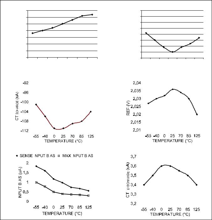
TYPICAL CHARACTERISTIC CURVES
VOUTS: Source connection of external N-channel MOSFET and sensed output voltage of load.
VPUMP: Charge pump output voltage. A capacitor should be tied between this pin and VOUTS with a typical value being 0.01 F.
Linear Amp VIO vs. Temperature |
Fault Threshold vs. Temperature |
|
3.5 |
|
|
|
|
|
|
|
3 |
|
|
|
|
|
|
IO (mV) |
2.5 |
|
|
|
|
|
|
2 |
|
|
|
|
|
|
|
1.5 |
|
|
|
|
|
|
|
V |
|
|
|
|
|
|
|
1 |
|
|
|
|
|
|
|
|
|
|
|
|
|
|
|
|
0.5 |
|
|
|
|
|
|
|
0 |
|
|
|
|
|
|
|
-55 |
-40 |
0 |
25 |
70 |
85 |
125 |
|
|
TEMPERATURE (°C) |
|
||||
(mV) |
-48 |
|
|
|
|
|
|
-48.5 |
|
|
|
|
|
|
|
-49 |
|
|
|
|
|
|
|
THRESHOLD |
|
|
|
|
|
|
|
-49.5 |
|
|
|
|
|
|
|
-50 |
|
|
|
|
|
|
|
-50.5 |
|
|
|
|
|
|
|
-51 |
|
|
|
|
|
|
|
FAULT |
|
|
|
|
|
|
|
-51.5 |
|
|
|
|
|
|
|
-52 |
|
|
|
|
|
|
|
|
|
|
|
|
|
|
|
|
-55 |
-40 |
0 |
25 |
70 |
85 |
125 |
|
|
TEMPERATURE (°C) |
|
||||
CT ICHARGE vs. Temperature |
|
VCC - REF vs Temperature |
|
||||||||||||||||||||||||||||
|
|
|
|
|
|
|
|
|
|
|
|
|
|
|
|
|
|
|
|
|
|
|
|
|
|
|
|
|
|
|
|
|
|
|
|
|
|
|
|
|
|
|
|
|
|
|
|
|
|
|
|
|
|
|
|
|
|
|
|
|
|
|
|
|
|
|
|
|
|
|
|
|
|
|
|
|
|
|
|
|
|
|
|
|
|
|
|
|
|
|
|
|
|
|
|
|
|
|
|
|
|
|
|
|
|
|
|
|
|
|
|
|
|
|
|
|
|
|
|
|
|
|
|
|
|
|
|
|
|
|
|
|
|
|
|
|
|
|
|
|
|
|
|
|
|
|
|
|
|
|
|
|
|
|
|
|
|
|
|
|
|
|
|
|
|
|
|
|
|
|
|
|
|
|
|
|
|
|
|
|
|
|
|
|
|
|
|
|
|
|
|
|
|
|
|
|
|
|
|
|
|
|
|
|
|
|
|
|
|
|
|
|
|
|
|
|
|
|
|
|
|
|
|
|
|
|
|
|
|
|
|
|
|
|
|
|
|
|
|
|
|
|
|
|
|
|
|
|
|
|
|
|
|
|
|
|
|
|
|
|
|
|
|
|
|
|
|
|
|
|
|
|
|
|
|
|
|
|
|
|
|
|
|
|
|
|
|
|
|
|
|
|
|
|
|
|
|
|
|
|
|
|
|
|
|
|
|
|
|
|
|
|
|
|
|
|
|
|
|
IMAX & SENSE Input Bias vs. Temperature |
|
|
|
|
CT IDISCHARGE vs. Temperature |
|
||||||||||||||||||||||||||||||||||||||||||||
|
|
|
|
|
|
|
|
|
|
|
|
|
|
|
|
|
|
|
|
|
|
|
|
|
|
|
|
|
|
|
|
|
|
|
|
|
|
|
|
|
|
|
|
|
|
|
|
|
|
|
|
|
|
|
|
|
|
|
|
|
|
|
|
|
|
|
|
|
|
|
|
|
|
|
|
|
|
|
|
|
|
|
|
|
|
|
|
|
|
|
|
|
|
|
|
|
|
|
|
|
|
|
|
|
|
|
|
|
|
|
|
|
|
|
|
|
|
|
|
|
|
|
|
|
|
|
|
|
|
|
|
|
|
|
|
|
|
|
|
|
|
|
|
|
|
|
|
|
|
|
|
|
|
|
|
|
|
|
|
|
|
|
|
|
|
|
|
|
|
|
|
|
|
|
|
|
|
|
|
|
|
|
|
|
|
|
|
|
|
|
|
|
|
|
|
|
|
|
|
|
|
|
|
|
|
|
|
|
|
|
|
|
|
|
|
|
|
|
|
|
|
|
|
|
|
|
|
|
|
|
|
|
|
|
|
|
|
|
|
|
|
|
|
|
|
|
|
|
|
|
|
|
|
|
|
|
|
|
|
|
|
|
|
|
|
|
|
|
|
|
|
|
|
|
|
|
|
|
|
|
|
|
|
|
|
|
|
|
|
|
|
|
|
|
|
|
|
|
|
|
|
|
|
|
|
|
|
|
|
|
|
|
|
|
|
|
|
|
|
|
|
|
|
|
|
|
|
|
|
|
|
|
|
|
|
|
|
|
|
|
|
|
|
|
|
|
|
|
|
|
|
|
|
|
|
|
|
|
|
|
|
|
|
|
|
|
|
|
|
|
|
|
|
|
|
|
|
|
|
|
|
|
|
|
|
|
|
|
|
|
|
|
|
|
|
|
|
|
|
|
|
|
|
|
|
|
|
|
|
|
|
|
|
|
|
|
|
|
|
|
|
|
|
|
|
|
|
|
|
|
|
|
|
|
|
|
|
|
|
|
|
|
|
|
|
|
|
|
|
|
|
|
|
|
|
|
|
|
|
|
|
|
|
|
|
|
|
|
|
|
|
|
|
|
|
|
|
|
|
|
|
|
|
|
|
|
|
|
|
|
|
|
|
|
|
|
|
|
|
|
|
|
|
|
|
|
|
|
|
|
|
|
|
|
|
|
|
|
|
|
|
|
|
|
|
|
|
|
|
|
|
|
|
|
|
|
|
|
|
|
|
|
|
|
|
|
|
|
|
|
|
|
|
|
|
|
|
|
|
|
|
|
|
|
|
|
|
|
|
|
|
|
|
|
|
|
|
|
|
|
|
|
|
|
|
|
|
|
|
|
|
|
|
|
|
|
|
|
|
|
|
|
|
|
|
|
|
|
|
|
|
|
|
|
|
|
|
|
|
|
|
|
|
|
|
|
|
|
|
|
|
|
|
|
|
|
|
|
|
|
|
|
|
|
|
|
|
|
|
|
|
|
|
|
|
|
|
|
|
|
|
|
|
|
|
|
|
|
|
|
|
|
|
|
|
|
|
|
|
|
|
|
|
|
|
|
|
|
|
|
|
|
|
|
|
|
|
|
|
|
|
|
|
|
|
|
|
|
|
|
|
|
|
|
|
|
|
|
|
|
|
|
|
|
|
|
|
|
|
|
|
|
|
|
|
|
|
|
|
|
|
|
|
|
|
|
|
|
|
|
|
|
|
|
|
|
|
|
|
|
|
|
|
|
Figure 1. Typical characteristic curves.
5
 Loading...