


UC3886N

6/98
Average Current Mode PWM Controller IC
BLOCK DIAGRAM
UC1886
UC2886
UC3886
UDG-95098-2
DESCRIPTION
The UC3886 family of PWM controller ICs is designed for DC-to-DC converters with average current mode control. It is designed for use in conjunction with the UC3910 4-bit DAC and Voltage Monitor. The UC3886
drives an external N-channel MOSFET and can be used to power the Intel Pentium® Pro and other high-end microprocessors.
The UC3886 in conjunction with the UC3910 converts 5VDC to an adjustable output ranging from 2.0V to 3.5V in 100mV steps with 35mV DC system accuracy.
The oscillator is programmed by the user’s selection of an external resistor and capacitor, and is designed for 300kHz typical operation.
The voltage and current amplifiers have 3.5MHz gain-bandwidth product
to satisfy high performance system requirements.
The internal current sense amplifier permits the use of a low value current
sense resistor, minimizing power loss. It has inputs and outputs accessible to allow user-selection of gain-setting resistors, and is internally compensated for a gain of 5 and above. The command voltage input is
buffered and provided for use as the reference for the current sense amplifier.
The output of the voltage amplifier (input to the current amplifier) is
clamped to 1 volt above the command voltage to serve as a current limit.
The gate output can be disabled by bringing the CAO/ENBL pin to below
0.8 volts.
FEATURES
• 10.3V - 20V Operating Range
• Low Offset Voltage Amplifier
• High Bandwidth Current and Voltage
Amplifiers
• Low Offset Current Sense Amplifier
• Undervoltage Lockout
• Trimmed 5 Volt Reference
• Externally Programmable Oscillator
Charge Current
• 1.5A Peak Totem Pole Output
• Available in 16-pin DIL or SOIC
Packages
2
UC1886
UC2886
UC3886
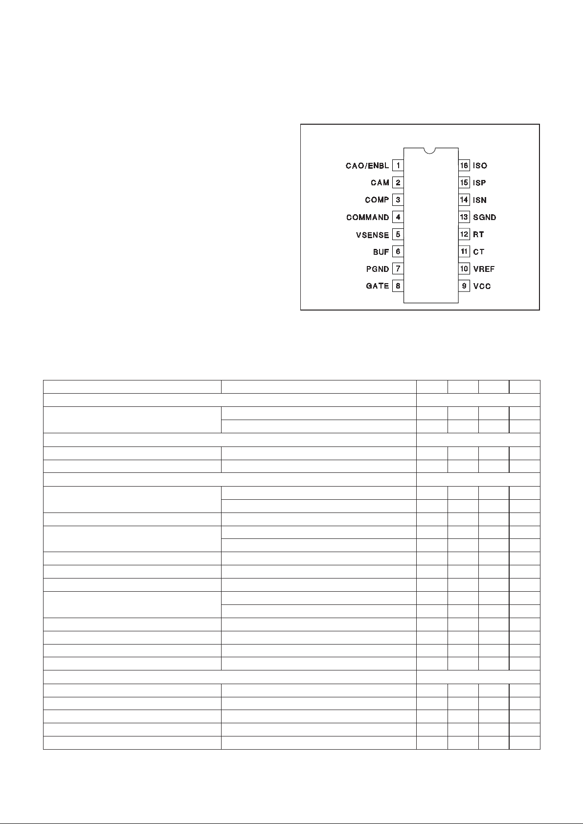
CONNECTION DIAGRAM
DIL-16, SOIC-16 (Top View)
J, N,or D Packages
ABSOLUTE MAXIMUM RATINGS
Supply Voltage ..................................20V
Output Current
CAM, COMMAND, VSENSE, ISN, ISP.............±1A
Analog Input ..............................–0.3V to 7V
Storage Temperature ...................–65°C to +150°C
Junction Temperature...................–55°C to +150°C
Lead Temperatue (Soldering, 10 sec.) .............+300°C
Currents are positive into,negative out of the specified terminal.
Consult Packaging Section of Databook for thermal limitations
and considerations of packages.
ELECTRICAL CHARACTERISTICS Unless otherwise specified, VCC = 12V, VCOMMAND = 3.0V, CT = 1nF, RT = 10k,
TA =TJ =0°C<TA < 70°C for the UC3886. (Note: –25°C < TA < 85°C for the UC2886, and –55°C < TA < 125°C for the UC1886)
PARAMETER TEST CONDITIONS MIN TYP MAX UNITS
Overall
Supply Current VCC = 11V, Gate Open 10 15 mA
VCC = 9.3V 5 mA
Undervoltage Lockout
Start Threshold 9.7 10.3 10.8 V
UVLO Hysteresis 0.25 0.4 V
Voltage Error Amplifier
Input Offset Voltage V
CM
= 3.0V (UC3886) 4 mV
VCM= 3.0V (UC2886, UC1886) 15 mV
Input Bias Current V
CM
= 3.0V −2 µA
Input Offset Current VCM= 3.0V (UC3886) 0.01 µA
VCM= 3.0V (UC2886, UC1886) 0.1 µA
Open Loop Gain 2.5V < V
COMP
< 3.5V 60 85 dB
Common-Mode Rejection Ratio 2V < V
COMP
<4V 60 85 dB
Power Supply Rejection Ratio 11V < VCC < 15V 60 85 dB
Output High Voltage (Clamp) I
COMP
= –100µA (UC3886) 3.95 4 4.05 V
I
COMP
= –100µA (UC2886, UC1886) 3.9 4.1 V
Output Low Voltage (Clamp) I
COMP
= 100µA 1.9 2.7 V
Output Sink Current V
COMP
= 3.7V 0.9 mA
Output Source Current V
COMP
= 2.8V –0.15 −0.25 mA
Gain-Bandwidth Product F = 100kHz 2 3.5 MHz
5.0V Reference
Output Voltage I
VREF
= 1.0mA 4.9 5 5.1 V
Total Variation Line, Load, Temperature 4.825 5.175 V
Line Regulation 11V < VCC < 15V 10 mV
Load Regulation 0 < I
VREF
< 2mA 15 mV
Short Circuit Current –10 −40 mA
3
UC1886
UC2886
UC3886
ELECTRICAL CHARACTERISTICS
Unless otherwise specified, VCC = 12V, VCOMMAND = 3.0V, CT = 1nF, RT = 10k,
TA =TJ =0°C<TA < 70°C for the UC3886. (Note: –25°C < TA < 85°C for the UC2886, and –55°C < TA < 125°C for the UC1886)
PARAMETER TEST CONDITIONS MIN TYP MAX UNITS
Input Buffer
Gain I
BUF
= ± 500µA (UC3886) 0.98 1 1.02 V/V
I
BUF
= ± 500µA (UC2886, UC1886) 0.95 1.05 V/V
Current-Sense Amplifier
Input Offset Voltage V
CM
= 3.0V (UC3886) 2 mV
VCM= 3.0V (UC2886, UC1886) 6 mV
Input Bias Current VCM= 3.0V -1 µA
Input Offset Current V
CM
= 3.0V 0.2 µA
Open Loop Gain 2V < V
ISO
<6V 60 85 dB
CMRR 0V < VCM< 4.5V 60 85 dB
PSRR 11V < VCC < 15V 60 85 dB
Output High Voltage I
ISO
= –100µA5V
Output Low Voltage I
ISO
= 1mA 1 V
Output Source Current V
ISO
=2V −0.2 mA
Gain-Bandwidth Product F = 100kHz 2 3.5 MHz
Current Amplifier
Input Offset Voltage V
CM
= 3.0V (UC3886) 13 mV
VCM= 3.0V (UC2886, UC1886) 18 mV
Input Bias Current VCM= 3.0V 1 µA
Open Loop Gain 1V < V
CAO
<3V 60 85 dB
CMRR 1.5V < VCM< 4.5V 60 85 dB
PSRR 11V < VCC < 15V 60 85 dB
Output High Voltage I
CAO
= –100µA 3 3.3 V
Output Low Voltage I
CAO
= 100µA1V
Output Source Current V
CAO
=1V −0.1 –0.25 mA
Gain-Bandwidth Product F = 100kHz 2 3.5 MHz
Oscillator
Frequency RT = 10k, CT = 1nF (UC3886) 90 100 110 kHz
RT = 10k, CT = 1nF (UC2886, UC1886) 85 115 kHz
Frequency Change With Voltage 11V > VCC > 15V 1 %
CT Peak Voltage 2.6 2.8 V
CT Valley Voltage 1 1.2 V
CT Peak-to-Peak Voltage 1.6 1.8 2.0 V
Output Section
Output Low Voltage I
GATE
= 200mA 1.6 2.2 V
Output High Voltage I
GATE
= –200mA 9 10.3 V
Output Low Voltage 5V < VCC < 9V, I
GATE
= 10mA 0.5 V
V
CAO
< 0.8V, I
GATE
= 10mA 0.5 V
Rise/Fall Time CL= 1nF 150 ns
Maximum Duty Cycle (UC3886) 90 %
(UC2886, UC1886) 85 %
 Loading...