


UC5181C
Octal Line Receiver
FEATURES
•Meets EIA232E/423A/422A and CCITT V.10, V.11, V.28, X.26, X.27
•Single +5V Supply—TTL Compatible Outputs
•Differential Inputs withstand ±25V
•Low Open Circuit Voltage for Improved Failsafe Characteristic
•Reduced Supply Current—35mA Max
•Internal Hysteresis
DESCRIPTION
The UC5181C is an octal line receiver designed to meet a wide range of digital communications requirements as outlined in EIA standards EIA232E, EIA422A, EIA423A and CCITT V.10, V.11, V.28, X.26, and X.27. The UC5181C is similar to the UC5180C, but without the input filtering. Thus, it covers the entire range of data rates up to 10MBPS. A failsafe function allows these devices to “fail” to a known state under a wide variety of fault conditions at the inputs.
ABSOLUTE MAXIMUM RATINGS (Note 1)
Supply Voltage, VCC . . . . . . . . . . . . . . . . . . . . . . . . . . . . . . . . . . . . . . . . . . . . 7V Output Sink Current. . . . . . . . . . . . . . . . . . . . . . . . . . . . . . . . . . . . . . . . . . 50mA Output Short Circuit Time . . . . . . . . . . . . . . . . . . . . . . . . . . . . . . . . . . . . . 1 Sec Common Mode Input Range. . . . . . . . . . . . . . . . . . . . . . . . . . . . . . . . . . . . . 15V Differential Input Range . . . . . . . . . . . . . . . . . . . . . . . . . . . . . . . . . . . . . . . . 25V Failsafe Voltage. . . . . . . . . . . . . . . . . . . . . . . . . . . . . . . . . . . . . . . . . -0.3 to VCC PLCC Power Dissipation, TA=25° C (Note 2) . . . . . . . . . . . . . . . . . . . 1000 mW DIP Power Dissipation, TA=25° C (Note 2) . . . . . . . . . . . . . . . . . . . . . 1200 mW Storage Temperature Range . . . . . . . . . . . . . . . . . . . . . . . . -65° C to +150° C Lead Temperature (Soldering, 10 seconds) . . . . . . . . . . . . . . . . . . . . . . -300° C
Note 1: All voltages are with respect to ground, pin 14. Currents are positive in, negative out of the specified terminal.
Note 2: Consult packaging section of Databook for thermal limitations and considerations of package.
CONNECTION DIAGRAMS
DIL-28 (TOP VIEW) |
|
PLCC-28 (TOP VIEW) |
||||||||||||||||||||||||||||||||||||||||||||||||||||||||||||||||||||||||||||||||||||||
|
|
|
|
|
|
|
|
|
|
|
|
|
|
|
|
|
|
|
|
|
|
|
|
|
|
|
|
|
|
|
|
|
|
|
|
|
|
|
|
|
|
|
|
|
|
|
|
|
|
|
|
|
|
|
|
|
|
|
|
|
|
|
|
|
|
|
|
|
|
|
|
|
|
|
|
|
|
|
|
|
|
|
|
|
|
|
|
|
|
|
|
|
|
|
|
|
|
|
|
|
|
|
|
|
|
|
|
|
|
|
|
|
|
|
|
|
|
|
|
|
|
|
|
|
|
|
|
|
|
|
|
|
|
|
|
|
|
|
|
|
|
|
|
|
|
|
|
|
|
|
|
|
|
|
|
|
|
|
|
|
|
|
|
|
|
|
|
|
|
|
|
|
|
|
|
|
|
|
|
|
|
|
|
|
|
|
|
|
|
|
|
|
|
|
|
|
|
|
|
|
|
|
|
|
|
|
|
|
|
|
|
|
|
|
|
|
|
|
|
|
|
|
|
|
|
|
|
|
|
|
|
|
|
|
|
|
|
|
|
|
|
|
|
|
|
|
|
|
|
|
|
|
|
|
|
|
|
|
|
|
|
|
|
|
|
|
|
|
|
|
|
|
|
|
|
|
|
|
|
|
|
|
|
|
|
|
|
|
|
|
|
|
|
|
|
|
|
|
|
|
|
|
|
|
|
|
|
|
|
|
|
|
|
|
|
|
|
|
|
|
|
|
|
|
|
|
|
|
|
|
|
|
|
|
|
|
|
|
|
|
|
|
|
|
|
|
|
|
|
|
|
|
|
|
|
|
|
|
|
|
|
|
|
|
|
|
|
|
|
|
|
|
|
|
|
|
|
|
|
|
|
|
|
|
|
|
|
|
|
|
|
|
|
|
|
|
|
|
|
|
|
|
|
|
|
|
|
|
|
|
|
|
|
|
|
|
|
|
|
|
|
|
|
|
|
|
|
|
|
|
|
|
|
|
|
|
|
|
|
|
|
|
|
|
|
|
|
|
|
|
|
|
|
|
|
|
|
|
|
|
|
|
|
|
|
|
|
|
|
|
|
|
|
|
|
|
|
|
|
|
|
|
|
|
|
|
|
|
|
|
|
|
|
|
|
|
|
|
|
|
|
|
|
|
|
|
|
|
|
|
|
|
|
|
|
|
|
|
|
|
|
|
|
|
|
|
|
|
|
|
|
|
|
|
|
|
|
|
|
|
|
|
|
|
|
|
|
|
|
|
|
|
|
|
|
|
|
|
|
|
|
|
|
|
|
|
|
|
|
|
|
|
|
|
|
|
|
|
|
|
|
|
|
|
|
|
|
|
|
|
|
|
|
|
|
|
|
|
|
|
|
|
|
|
|
|
|
|
|
|
|
|
|
|
|
|
|
|
|
|
|
|
|
|
|
|
|
|
|
|
|
|
|
|
|
|
|
|
|
|
|
|
|
|
|
|
|
|
|
|
|
|
|
|
|
|
|
|
|
|
|
|
|
|
|
|
|
|
|
|
|
|
|
|
|
|
|
|
|
|
|
|
|
|
|
|
|
|
|
|
|
|
|
|
|
|
|
|
|
|
|
|
|
|
|
|
|
|
|
|
|
|
|
|
|
|
|
|
|
|
|
|
|
|
|
|
|
|
|
|
|
|
|
|
|
|
|
|
|
|
|
|
|
|
|
|
|
|
|
|
|
|
|
|
|
|
|
|
|
|
|
|
|
|
|
|
|
|
|
|
|
|
|
|
|
|
|
|
|
|
|
|
|
|
|
|
|
|
|
|
|
|
|
|
|
|
|
|
|
|
|
|
|
|
|
|
|
|
|
|
|
|
|
|
|
|
|
|
|
|
|
|
|
|
|
|
|
|
|
|
|
|
|
|
|
|
|
|
|
|
|
|
|
|
|
|
|
|
|
|
|
|
|
|
|
|
|
|
|
|
|
|
|
|
|
|
|
|
|
|
|
|
|
|
|
|
|
|
|
|
|
|
|
|
|
|
|
|
|
|
|
|
|
|
|
|
|
|
|
|
|
|
|
|
|
|
|
|
|
|
|
|
|
|
|
|
|
|
|
|
|
|
|
|
|
|
|
|
|
|
|
|
|
|
|
|
|
|
|
|
|
|
|
|
|
|
|
|
|
|
|
|
|
|
|
|
|
|
|
|
|
|
|
|
|
|
|
|
|
|
|
|
|
|
|
|
|
|
|
|
|
|
|
|
|
|
|
|
|
|
|
|
|
|
|
|
|
|
|
|
|
|
|
|
|
|
|
|
|
|
|
|
|
|
|
|
|
|
|
|
|
|
|
|
|
|
|
|
|
|
|
|
|
|
|
|
|
|
|
|
|
|
|
|
|
|
|
|
|
|
|
|
|
|
|
|
|
|
|
|
|
|
|
|
|
|
|
|
|
|
|
|
|
|
|
|
|
|
|
|
|
|
|
|
|
|
|
|
|
|
|
|
|
|
|
|
|
|
|
|
|
|
|
|
|
|
|
|
|
|
|
|
|
|
|
|
|
|
|
|
|
|
|
|
|
|
|
|
|
|
|
|
|
|
|
|
|
|
|
|
|
|
|
|
|
|
|
|
|
|
|
|
|
|
|
|
1/94
UC5181C
DC ELECTRICAL CHARACTERISTICS: Unless otherwise stated, these specifications apply for TA = 0°C to +70°C; VCC |
|||||||
|
|
= 5V ±5%, Input Common Mode Range ±7V, TA=TJ. |
|
|
|
||
|
|
|
|
|
|
|
|
PARAMETER |
SYMBOL |
TEST CONDITIONS |
|
UC5181C |
UNITS |
||
|
|
|
|
|
MIN |
MAX |
|
DC Input Resistance |
RIN |
3V ≤ |VIN|≤25V |
|
|
3 |
7 |
kΩ |
Failsafe Output Voltage |
VOFS |
Inputs Open or Shorted |
0≥IOUT≤8mAVFAILSAFE=0V |
|
0.45 |
V |
|
|
|
Together, or One Input Open |
0≥IOUT≥-400µA, VFAILSAFE=VCC |
2.7 |
|
|
|
|
|
and One Grounded |
|
|
|
||
|
|
|
|
|
|
|
|
|
|
|
|
|
|
|
|
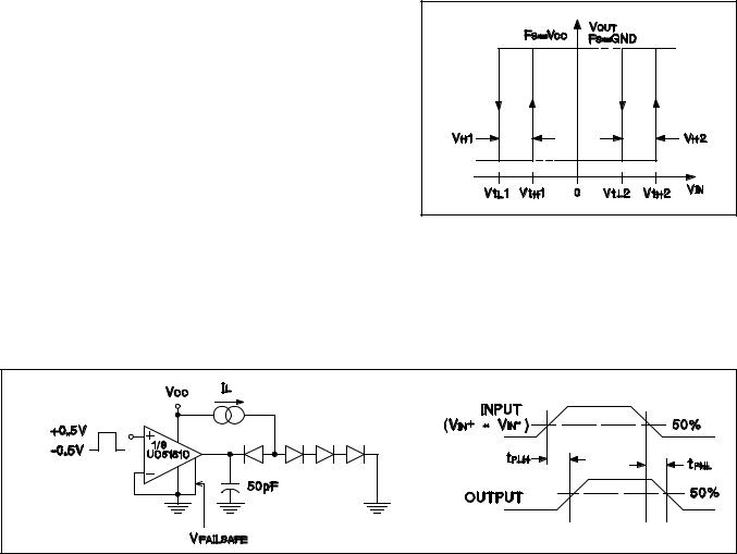
Differential Input High |
VTL |
VOUT= 0.45V, IOUT = -440µA (See Figure |
RS = 0 (Note3) |
50 |
200 |
mV |
|
Threshold |
|
1) |
|
RS = 500 (Note 3) |
|
400 |
|
Differential Input Low |
VTL |
VOUT = 0.45V, IOUT = 8 mA (See Figure |
RS = 0 (Note 3) |
-200 |
-50 |
mV |
|
Threshold |
|
1) |
|
RS = 500 (Note 3) |
-400 |
|
|
Hysteresis |
VH |
FS=0V or VCC (See Figure 1) |
|
|
45 |
140 |
mV |
Open Circuit Input Voltage |
VIOC |
|
|
|
|
75 |
mV |
Input Capacitance |
CI |
|
|
|
|
20 |
pF |
High Level Output Voltage |
VOH |
VID = 1V, IOUT = -440 µA |
|
|
2.7 |
|
V |
Low Level Output Voltage |
VOL |
VID = -1V (Note 4) |
|
IOUT = 4 mA |
|
0.4 |
V |
|
|
|
IOUT = 8 mA |
|
0.45 |
|
|
|
|
|
|
|
|
||
Short Circuit Output |
IOS |
Note 5 |
|
|
20 |
100 |
mA |
Current |
|
|
|
|
|
|
|
Supply current |
ICC |
4.75V ≤VCC≤5.25V |
|
|
|
35 |
mA |
Input Current |
IIN |
Other Inputs Grounded |
|
VIN = +10V |
|
3.25 |
mA |
|
|
|
VIH = -10V |
-3.25 |
|
|
|
|
|
|
|
|
|
||
Note 3: RS is a resistor in series with each input. Note 4: Measure after 100 ms warm up (at 0°C).
Note 5: Only 1 output may be shorted at a time and then only for a maximum of 1 sec.
Note 6: The delays, either tPLH or tPHL, shall not vary from receiver to receiver by more than 35ns.
Figure 1. VTL, VTH,VH Definition
AC ELECTRICAL CHARACTERISTICS: VCC=5V ±5%. TA=0°C to +70°C, Figure 2 TA=TJ.
PARAMETER |
SYMBOL |
TEST CONDITIONS |
UC5181C |
UNITS |
|
|
|
|
MIN |
MAX |
|
Propagation Delay–Low to High |
tPLH |
CL=50pF, VIN= ±500 mV (Note 6) |
|
120 |
ns |
Propagation Delay–High to Low |
tPHL |
CL=50pF, VIN= ±500 mV (Note 6) |
|
120 |
ns |
Acceptable Input frequency |
fA |
Unused Input Grounded, VIN= ±200 mV |
|
5.0 |
MHz |
Figure 2. AC Test Circuit |
2 |
 Loading...