


Texas Instruments UC3909QTR, UC3909Q, UC3909N, UC3909DWTR, UC3909DW Datasheet
...
UC2909
UC3909
Switchmode Lead-Acid Battery Charger
FEATURES
∙Accurate and Efficient Control of Battery Charging
∙Average Current Mode Control from Trickle to Overcharge
∙Resistor Programmable Charge Currents
∙Thermistor Interface Tracks Battery Requirements Over Temperature
∙Output Status Bits Report on Four Internal Charge States
∙Undervoltage Lockout Monitors VCC and VREF
DESCRIPTION
The UC3909 family of Switchmode Lead-Acid Battery Chargers accurately controls lead acid battery charging with a highly efficient average current mode control loop. This chip combines charge state logic with average current PWM control circuitry. Charge state logic commands current or voltage control depending on the charge state. The chip includes undervoltage lockout circuitry to insure sufficient supply voltage is present before output switching starts. Additional circuit blocks include a differential current sense amplifier, a 1.5% voltage reference, a –3.9mV/°C thermistor linearization circuit, voltage and current error amplifiers, a PWM oscillator, a PWM comparator, a PWM latch, charge state decode bits, and a 100mA open collector output driver.
BLOCK DIAGRAM
UDG-95007-1
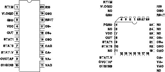
Pin numbers refer to J, N, DW packages.
1/99
UC2909
UC3909
ABSOLUTE MAXIMUM RATINGS
Supply Voltage (VCC), OUT, STAT0, STAT1 . |
. . . . . . . . . . 40V |
|
Output Current Sink . . . . . . . . . . . . . . . . . |
. . . . |
. . . . . . . . . 0.1A |
CS+, CS- . . . . . . . . . . . . . . . . . . . . . . . . . . |
-0.4 to VCC (Note 1) |
|
Remaining Pin Voltages. . . . . . . . . . . . . . . |
. . . . |
. . . -0.3V to 9V |
Storage Temperature . . . . . . . . . . . . . . . . |
. . . |
- 65°C to +150°C |
Junction Temperature . . . . . . . . . . . . . . . . |
. . . |
- 55°C to +150°C |
Lead Temperature (Soldering, 10 sec.) . . . |
. . . . |
. . . . . . +300°C |
All currents are positive into, negative out of the specified terminal. Consult Packaging Section of Databook for thermal limitations and considerations of packages.
Note 1: Voltages more negative than -0.4V can be tolerated if current is limited to 50mA.
CONNECTION DIAGRAMS
DIL-20, (Top View) |
|
|
|
|
|
|
|
|
|
LCC-28, PLCC-28 (Top View) |
|
|
|
|
|
|
|
|
||||||||||||||||||||||||||||||||||||||||||||||||||||||||||||||||||
J or N, DW Packages |
|
|
|
|
|
|
|
|
|
L, Q Packages |
|
|
|
|
|
|
|
|
||||||||||||||||||||||||||||||||||||||||||||||||||||||||||||||||||
|
|
|
|
|
|
|
|
|
|
|
|
|
|
|
|
|
|
|
|
|
|
|
|
|
|
|
|
|
|
|
|
|
|
|
|
|
|
|
|
|
|
|
|
|
|
|
|
|
|
|
|
|
|
|
|
|
|
|
|
|
|
|
|
|
|
|
|
|
|
|
|
|
|
|
|
|
|
|
|
|
|
|
|
|
|
|
|
|
|
|
|
|
|
|
|
|
|
|
|
|
|
|
|
|
|
|
|
|
|
|
|
|
|
|
|
|
|
|
|
|
|
|
|
|
|
|
|
|
|
|
|
|
|
|
|
|
|
|
|
|
|
|
|
|
|
|
|
|
|
|
|
|
|
|
|
|
|
|
|
|
|
|
|
|
|
|
|
|
|
|
|
|
|
|
|
|
|
|
|
|
|
|
|
|
|
|
|
|
|
|
|
|
|
|
|
|
|
|
|
|
|
|
|
|
|
|
|
|
|
|
|
|
|
|
|
|
|
|
|
|
|
|
|
|
|
|
|
|
|
|
|
|
|
|
|
|
|
|
|
|
|
|
|
|
|
|
|
|
|
|
|
|
|
|
|
|
|
|
|
|
|
|
|
|
|
|
|
|
|
|
|
|
|
|
|
|
|
|
|
|
|
|
|
|
|
|
|
|
|
|
|
|
|
|
|
|
|
|
|
|
|
|
|
|
|
|
|
|
|
|
|
|
|
|
|
|
|
|
|
|
|
|
|
|
|
|
|
|
|
|
|
|
|
|
|
|
|
|
|
|
|
|
|
|
|
|
|
|
|
|
|
|
|
|
|
|
|
|
|
|
|
|
|
|
|
|
|
|
|
|
|
|
|
|
|
|
|
|
|
|
|
|
|
|
|
|
|
|
|
|
|
|
|
|
|
|
|
|
|
|
|
|
|
|
|
|
|
|
|
|
|
|
|
|
|
|
|
|
|
|
|
|
|
|
|
|
|
|
|
|
|
|
|
|
|
|
|
|
|
|
|
|
|
|
|
|
|
|
|
|
|
|
|
|
|
|
|
|
|
|
|
|
|
|
|
|
|
|
|
|
|
|
|
|
|
|
|
|
|
|
|
|
|
|
|
|
|
|
|
|
|
|
|
|
|
|
|
|
|
|
|
|
|
|
|
|
|
|
|
|
|
|
|
|
|
|
|
|
|
|
|
|
|
|
|
|
|
|
|
|
|
|
|
|
|
|
|
|
|
|
|
|
|
|
|
|
|
|
|
|
|
|
|
|
|
|
|
|
|
|
|
|
|
|
|
|
|
|
|
|
|
|
|
|
|
|
|
|
|
|
|
|
|
|
|
|
|
|
|
|
|
|
|
|
|
|
|
|
|
|
|
|
|
|
|
|
|
|
|
|
|
|
|
|
|
|
|
|
|
|
|
|
|
|
|
|
|
|
|
|
|
|
|
|
|
|
|
|
|
|
|
|
|
|
|
|
|
|
|
|
|
|
|
|
|
|
|
|
|
|
|
|
|
|
|
|
|
|
|
|
|
|
|
|
|
|
|
|
|
|
|
|
|
|
|
|
|
|
|
|
|
|
|
|
|
|
|
|
|
|
|
|
|
|
|
|
|
|
|
|
|
|
|
|
|
|
|
|
|
|
|
|
|
|
|
|
|
|
|
|
|
|
|
|
|
|
|
|
|
|
|
|
|
|
|
|
|
|
|
|
|
|
|
|
|
|
|
|
|
|
|
|
|
|
|
|
|
|
|
|
|
|
|
|
|
|
|
|
|
|
|
|
|
|
|
|
|
|
|
|
|
|
|
|
|
|
|
|
|
|
|
|
|
|
|
|
|
|
|
|
|
|
|
|
|
|
|
|
|
|
|
|
|
|
|
|
|
|
|
|
|
|
|
|
|
|
|
|
|
|
|
|
|
|
|
|
|
|
|
|
|
|
|
|
|
|
|
|
|
|
|
|
|
|
|
|
|
|
|
|
|
|
|
|
|
|
|
|
|
|
|
|
|
|
|
|
|
|
|
|
|
|
|
|
|
|
|
|
|
|
|
|
|
|
|
|
|
|
|
|
|
|
|
|
|
|
|
|
|
|
|
|
|
|
|
|
|
|
|
|
|
|
|
|
|
|
|
|
|
|
|
|
|
|
|
|
|
|
|
|
|
|
|
|
|
|
|
|
|
|
|
|
|
|
|
|
|
|
|
|
|
|
|
|
|
|
|
|
|
|
|
|
|
|
|
|
|
|
|
|
|
|
|
|
|
|
|
|
|
|
|
|
|
|
|
|
|
|
|
|
|
|
|
|
|
|
|
|
|
|
|
|
|
|
|
|
|
|
|
|
|
|
|
|
|
|
|
|
|
|
|
|
|
|
|
|
|
|
|
|
|
|
|
|
|
|
|
|
|
|
|
|
|
|
|
|
|
|
|
|
|
|
|
|
|
|
|
|
|
|
|
|
|
|
|
|
|
|
|
|
|
|
|
|
|
|
|
|
|
|
|
|
|
|
|
|
|
|
|
|
|
|
|
|
|
|
|
|
|
|
|
|
|
|
|
|
|
|
|
|
|
|
|
|
|
|
|
|
|
|
|
|
|
|
|
|
|
|
|
|
|
|
|
|
|
|
|
|
|
|
|
|
|
|
|
|
|
|
|
|
|
|
|
|
|
|
|
|
|
|
|
|
|
|
|
|
|
|
|
|
|
|
|
|
|
|
|
|
|
|
|
|
|
|
|
|
|
|
|
|
|
|
|
|
|
|
|
|
|
|
|
|
|
|
|
|
|
|
|
|
|
|
|
|
|
|
|
|
|
|
|
|
|
|
|
|
|
|
|
|
|
|
|
|
|
|
|
|
|
|
|
|
|
|
|
|
|
|
|
|
|
|
|
|
|
|
|
|
|
|
|
|
|
|
|
|
|
|
|
|
|
|
|
|
|
|
|
|
|
|
|
|
|
|
|
|
|
|
|
|
|
|
|
|
|
|
|
|
|
|
|
|
|
|
|
|
|
|
|
|
|
|
|
|
|
|
|
|
|
|
|
|
|
|
|
|
|
|
|
|
|
|
|
|
|
|
|
|
|
|
|
|
|
|
|
|
|
|
|
|
|
|
|
|
|
|
|
|
|
|
|
|
|
|
|
|
|
|
|
|
|
|
|
|
|
|
|
|
|
|
|
|
|
|
|
|
|
|
|
|
|
|
|
|
|
|
|
|
|
|
|
|
|
|
|
|
|
|
|
|
|
|
|
|
|
|
|
|
|
|
|
|
|
|
|
|
|
|
|
|
|
|
|
|
|
|
|
|
|
|
|
|
|
|
|
|
|
|
|
|
|
|
|
|
|
|
|
|
|
|
|
|
|
|
|
|
|
|
|
|
|
|
|
|
|
|
|
|
|
|
|
|
|
|
|
|
|
|
|
|
|
|
|
|
|
|
|
|
|
|
|
|
|
|
|
|
|
|
|
|
|
|
|
|
|
|
|
|
|
|
|
|
|
|
|
|
|
|
|
|
|
|
|
|
|
|
|
|
|
|
|
|
|
|
|
|
|
|
|
|
|
|
|
|
|
|
|
|
|
|
|
|
|
|
|
|
|
|
|
|
|
|
|
|
|
|
|
|
|
|
|
|
|
|
|
|
|
|
|
|
|
|
|
|
ELECTRICAL CHARACTERISTICS: Unless otherwise stated these specifications apply for TA = –40°C to +85°C for
UC2909; °0C to +70°C for UC3909; C T = 330pF, RSET = 11.5k, R10 = 10k, RTHM = 10k, VCC = 15V, Output no load, RSTAT0 = RSTAT1 = 10k, CHGENB = OVCTAP = VLOGIC, TA = TJ.
PARAMETER |
TEST CONDITIONS |
MIN |
TYP |
MAX |
UNITS |
Current Sense AMP (CSA) Section |
VID = CS+ – CS– |
|
|
|
|
DC Gain |
CS– = 0, CS+ = -50mV; CS+ = –250mV |
4.90 |
5 |
5.10 |
V/V |
|
CS+ = 0, CS– = 50mV; CS–- = 250mV |
4.90 |
5 |
5.10 |
V/V |
VOFFSET (VCSO – VCAO) |
CS+ = CS– = 2.3V, CAO = CA– |
|
|
15 |
mV |
CMRR |
VCM = –0.25 to VCC – 2, 8.8 < VCC < 14 |
50 |
|
|
dB |
|
VCM = –0.25 to VCC, 14 < VCC < 35 |
50 |
|
|
dB |
VOL |
VID = –550mV, –0.25V < VCM < VCC–2, |
|
0.3 |
0.6 |
V |
|
IO = 500μA |
|
|
|
|
VOH |
VID = +700mV, –0.25V < VCM < VCC–2, |
5.2 |
5.7 |
6.2 |
V |
|
IO = –250μA |
|
|
|
|
Output Source Current |
VID = +700mV, CSO = 4V |
|
–1 |
–0.5 |
mA |
Output Sink Current |
VID = –550mV, CSO = 1V |
3 |
4.5 |
|
mA |
3dB Bandwidth |
VID = 90mV, VCM = 0V |
200 |
|
|
kHz |
2
UC2909
UC3909
ELECTRICAL CHARACTERISTICS: Unless otherwise stated these specifications apply for TA = –40°C to +85°C for
UC2909; °0C to +70°C for UC3909; C T = 330pF, RSET = 11.5k, R10 = 10k, RTHM = 10k, VCC = 15V, Output no load, RSTAT0 = RSTAT1 = 10k, CHGENB = OVCTAP = VLOGIC, TA = TJ.
PARAMETER |
TEST CONDITIONS |
MIN |
TYP |
MAX |
UNITS |
Current Error Amplifier (CEA) Section |
|
|
|
|
|
IB |
8.8V < VCC < 35V, VCHGENB = VLOGIC |
|
0.1 |
0.8 |
μA |
VIO (Note 2) |
8.8V < VCC < 35V, CAO = CA– |
|
|
10 |
mV |
AVO |
1V < VAO < 4V |
60 |
90 |
|
dB |
GBW |
TJ = 25°C, F = 100kHz |
1 |
1.5 |
|
MHz |
VOL |
IO = 250μA |
|
0.4 |
0.6 |
V |
VOH |
IO = –5mA |
4.5 |
5 |
|
V |
Output Source Current |
CAO = 4V |
|
–25 |
–12 |
mA |
Output Sink Current |
CAO = 1V |
2 |
3 |
|
mA |
ICA–, ITRCK_CONTROL |
VCHGENB = GND |
8.5 |
10 |
11.5 |
μA |
Voltage Amplifier (CEA) Section |
|
|
|
|
|
IB |
Total Bias Current; Regulating Level |
|
0.1 |
1 |
μA |
VIO (Note 2) |
8.8V < VCC < 35V, VCM = 2.3V, VAO = VA– |
|
1.2 |
|
mV |
AVO |
1V < CAO < 4V |
60 |
90 |
|
dB |
GBW |
TJ = 25°C, F = 100kHz |
0.25 |
0.5 |
|
MHz |
VOL |
IO = 500μA |
|
0.4 |
0.6 |
V |
VOH |
IO = –500μA |
4.75 |
5 |
5.25 |
V |
Output Source Current |
CAO = 4V |
–2 |
–1 |
|
mA |
Output Sink Current |
CAO = 1V |
2 |
2.5 |
|
mA |
VAO Leakage: High Impedance State |
VCHGENB = GND, STAT0 = 0 & STAT1 = 0, |
–1 |
|
1 |
μA |
|
VAO = 2.3V |
|
|
|
|
Pulse Width Modulator Section |
|
|
|
|
|
Maximum Duty Cycle |
CAO = 0.6V |
90 |
95 |
100 |
% |
Modulator Gain |
CAO = 2.5V, 3.2V |
63 |
71 |
80 |
%/V |
OSC Peak |
|
|
3 |
|
V |
OSC Valley |
|
|
1 |
|
V |
Oscillator Section |
|
|
|
|
|
Frequency |
8.8V < VCC < 35V |
198 |
220 |
242 |
kHz |
Thermistor Derived Reference Section |
VID = VRTHM – VR10 |
|
|
|
|
Initial Accuracy, VAO (RTHM = 10k) |
VID = 0, R10 = RTHM =10k (Note 3) |
2.2655 |
2.3 |
2.3345 |
V |
|
VID = 0, R10 = RTHM =10k, –40°C ≤TA < 0°C |
2.254 |
2.3 |
2.346 |
V |
|
(Note 3) |
|
|
|
|
Line Regulation |
VCC = 8.8V to 35V |
|
3 |
10 |
mV |
VAO |
RTHM = 138k, R10 = 10k |
2.458 |
2.495 |
2.532 |
V |
|
RTHM = 138k, R10 = 10k, -40°C ≤ TA < 0°C |
2.445 |
2.495 |
2.545 |
V |
|
RTHM = 33.63k, R10 = 10k |
2.362 |
2.398 |
2.434 |
V |
|
RTHM = 33.63k, R10 = 10k, -40°C ≤ TA < 0°C |
2.350 |
2.398 |
2.446 |
V |
|
RTHM = 1.014k, R10 = 10k |
2.035 |
2.066 |
2.097 |
V |
|
RTHM = 1.014k, R10 = 10k, -40°C ≤ TA < 0°C |
2.025 |
2.066 |
2.107 |
V |
Charge Enable Comparator Section (CEC) |
|
|
|
|
|
Threshold Voltage |
As a function of VA– |
0.99 |
1 |
1.01 |
V/V |
Input Bias Current |
CHGENB = 2.3V |
–0.5 |
–0.1 |
|
μA |
3
 Loading...