


UCC27221
UCC27221 UCC27222
SLUS486B − AUGUST 2001 − REVISED JULY 2003
HIGH EFFICIENCY PREDICTIVE SYNCHRONOUS BUCK DRIVER
FEATURES |
APPLICATIONS |
DMaximizes Efficiency by Minimizing Body-Diode Conduction and Reverse Recovery Losses
DTransparent Synchronous Buck Gate Drive Operation From the Single Ended PWM Input Signal
D12-V or 5-V Input Operation
D3.3-V Input Operation With Availability of
12-V Bus Bias
DOn-Board 6.5-V Gate Drive Regulator
D±3.3-A TrueDrive Gate Drives for High
Current Delivery at MOSFET Miller Thresholds
DAutomatically Adjusts for Changing Operating Conditions
DThermally Enhanced 14-Pin PowerPAD
HTSSOP Package Minimizes Board Area and Junction Temperature Rise
FUNCTIONAL APPLICATION DIAGRAM
DNon-Isolated Single or Multi-phased DC-to-DC Converters for Processor Power, General Computer, Telecom and Datacom Applications
DESCRIPTION
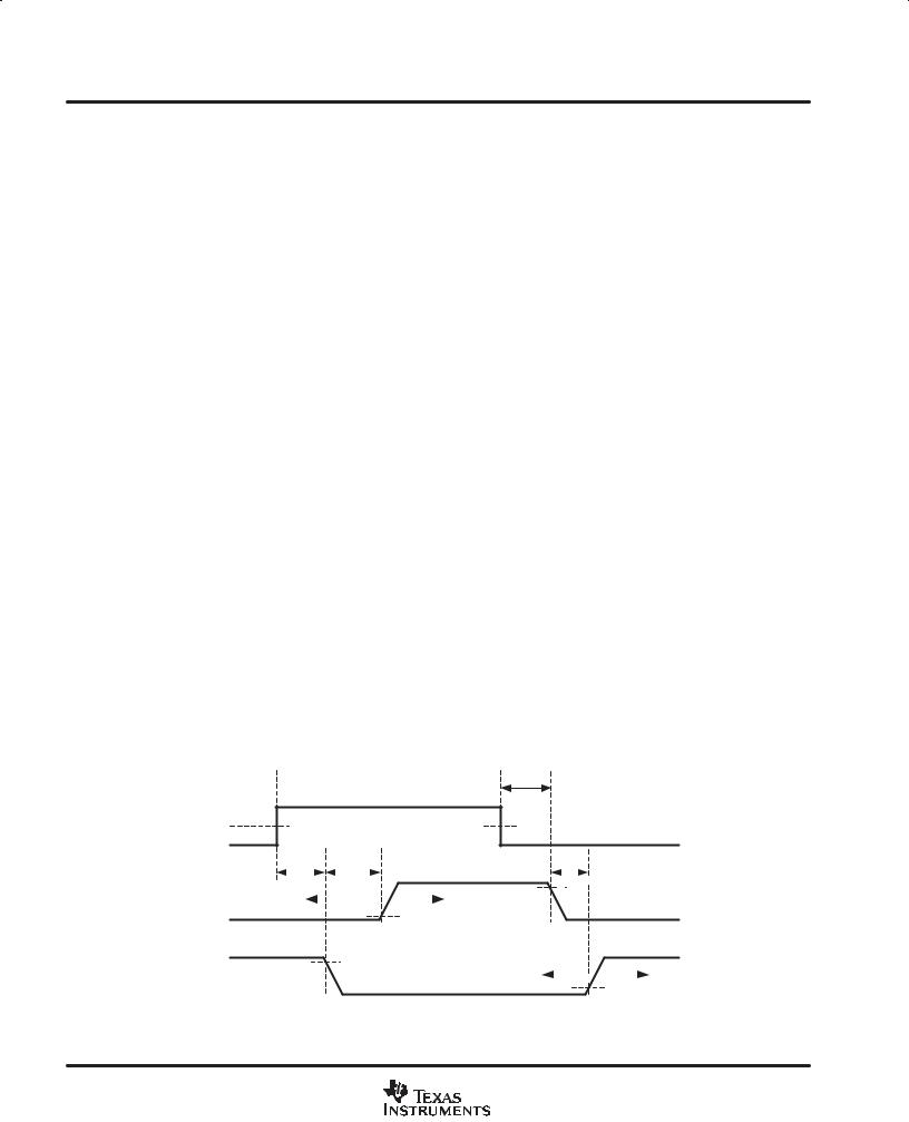
The UCC27221 and UCC27222 are high-speed synchronous buck drivers for today’s high-efficiency, lower-output voltage designs. Using Predictive Gate Drivet (PGD) control technology, these drivers reduce diode conduction and reverse recovery losses in the synchronous rectifier MOSFET(s). The UCC27221 has an inverted PWM input while the UCC27222 has a non-inverting PWM input.
Predictive Gate Drivet technology uses control loops which are stabilized internally and are therefore transparent to the user. These loops use no external components, so no additional design is needed to take advantage of the higher efficiency of these drivers.
VIN |
|
|
|
|
UCC27222 |
|
|
7 |
IN |
VHI |
14 |
PWMIN |
|
|
|
6,8 |
GND |
G1 |
13 |
3 |
VDD |
|
VOUT |
|
|
SW |
11,12 |
4,5 |
VLO |
G2 |
9,10 |
|
|
||
GNDIN GNDOUT
Note: 12-V input system shown. For 5-V input only systems, see Figure 6.
This closed loop feedback system detects body-diode conduction, and adjusts deadtime delays to minimize the conduction time interval. This virtually eliminates body-diode conduction while adjusting for temperature, loaddependent delays, and for different MOSFETs. Precise gate timing at the nanosecond level reduces the reverse recovery time of the synchronous rectifier MOSFET body-diode, reducing reverse recovery losses seen in the main (high-side) MOSFET. The lower junction temperature in the low-side MOSFET increases product reliability. Since the power dissipation is minimized, a higher switching frequency can also be used, allowing for smaller component sizes.
The UCC27221 and UCC27222 are offered in the thermally enhanced 14-pin PowerPADt package with 2°C/W θjc.
Predictive Gate Drivet and PowerPADt are trademarks of Texas Instruments Incorporated.
|
|
|
PRODUCTION DATA information is current as of publication date. |
Copyright 2002, Texas Instruments Incorporated |
|
Products conform to specifications per the terms of Texas Instruments |
|
|
standard warranty. Production processing does not necessarily include |
|
|
testing of all parameters. |
|
|
www.ti.com |
1 |

UCC27221
UCC27222
SLUS486B − AUGUST 2001 − REVISED JULY 2003
PWP PACKAGE
(TOP VIEW)
N/C |
|
|
1 |
14 |
|
|
VHI |
|
|
|
|
||||
N/C |
|
2 |
13 |
|
|
G1 |
|
|
|
|
|
||||
VDD |
|
3 |
12 |
|
|
SW |
|
|
|
|
|
||||
VLO |
|
4 |
11 |
|
|
SWS |
|
|
|
|
|
||||
PVLO |
|
5 |
10 |
|
|
G2S |
|
|
|
|
|
||||
AGND |
|
|
6 |
9 |
|
|
G2 |
|
|
|
|
||||
|
|
|
|||||
IN |
|
7 |
8 |
|
|
PGND |
|
|
|
|
|
||||
|
|
|
|
|
|
|
|
N/C − No internal connection
AVAILABLE OPTIONS
|
PWM INPUT |
PACKAGED DEVICES |
|
TA |
PowerPADt |
||
(IN) |
|||
|
|
HTSSOP−14 (PWP) |
|
−40 _C to 105_C |
INVERTING |
UCC27221PWP |
|
NON-INVERTING |
UCC27222PWP |
||
|
{The PWP package is available taped and reeled. Add R suffix to device type (e.g. UCC27221PWPR) to order quantities of 2,000 devices per reel and 90 units per tube.
absolute maximum ratings over operating free-air temperature (unless otherwise noted)† }
Supply voltage range, VDD . . . . . . . . . . . . . . . . . . . . . . . . . . . . . . . . . |
. . . . . . . . . . . . . . . . . . . . . . . |
. . . −0.3 to 20 V |
Input voltage, VHI . . . . . . . . . . . . . . . . . . . . . . . . . . . . . . . . . . . . . . . . . |
. . . . . . . . . . . . . . . . . . . . . . . |
. . . . . . . . . . 30 V |
SW, SWS . . . . . . . . . . . . . . . . . . . . . . . . . . . . . . . . . . . . . |
. . . . . . . . . . . . . . . . . . . . . . . |
. . . . . . . . . 20 V |
Supply current, IDD, including gate drive current . . . . . . . . . . . . . . . . |
. . . . . . . . . . . . . . . . . . . . . . . |
. . . . . . .100 mA |
Sink current (peak) pulsed, G1/G2 . . . . . . . . . . . . . . . . . . . . . . . . . . . |
. . . . . . . . . . . . . . . . . . . . . . . |
. . . . . . . . 4.0 A |
Source current (peak) pulsed, G1/G2 . . . . . . . . . . . . . . . . . . . . . . . . . |
. . . . . . . . . . . . . . . . . . . . . . . |
. . . . . . . −4.0 A |
Analog input, IN . . . . . . . . . . . . . . . . . . . . . . . . . . . . . . . . . . . . . . . . . . |
−3.0 V to V DD + 0.3 V, not to exceed 15 V |
|
Power Dissipation at TA = 25°C (PWP package) . . . . . . . . . . . . . . . . |
. . . . . . . . . . . . . . . . . . . . . . . |
. . . . . . . . . 3 W |
Operating junction temperature range, TJ . . . . . . . . . . . . . . . . . . . . . . |
. . . . . . . . . . . . . . . . . . . . . . |
−55 °C to 115°C |
Storage temperature range, Tstg . . . . . . . . . . . . . . . . . . . . . . . . . . . . . . |
. . . . . . . . . . . . . . . . . . . . . . |
−65 °C to 150°C |
Lead temperature soldering 1.6 mm (1/16 inch) from case for 10 seconds . . . . . . . . . . . . . . . . |
. . . . . . . 300°C |
|
†Stresses beyond those listed under “absolute maximum ratings” may cause permanent damage to the device. These are stress ratings only, and functional operation of the device at these or any other conditions beyond those indicated under “recommended operating conditions” is not implied. Exposure to absolute-maximum-rated conditions for extended periods may affect device reliability.
‡ All voltages are with respect to AGND and PGND. Currents are positive into, negative out of the specified terminal.
2 |
www.ti.com |
UCC27221
UCC27222
SLUS486B − AUGUST 2001 − REVISED JULY 2003
ELECTRICAL CHARACTERISTICS
VDD = 12-V, 1- F capacitor from VDD to GND, 1- F capacitor from VHI to SW, 0.1- F and 2.2- F capacitor from PVLO to PGND, PVLO tied to
VLO, TA = −40 _C to 105_C for the UCC2722x, TA = TJ (unless otherwise noted)
VLO regulator
PARAMETER |
|
TEST CONDITIONS |
MIN |
TYP |
MAX |
UNIT |
|
|
|
|
|
|
|
|
|
|
VDD = 12 |
V, |
IVLO = 0 mA |
6.2 |
6.5 |
6.8 |
|
Regulator output voltage |
VDD = 20 |
V, |
IVLO = 0 mA |
6.2 |
6.5 |
6.8 |
V |
|
VDD = 8.5 V, |
IVLO = 100 mA |
6.1 |
6.5 |
6.9 |
|
|
Line Regulation |
VDD = 12 |
V to 20 V |
|
|
2 |
10 |
mV |
Load Regulation |
IVLO = 0 mA to 100 mA |
|
|
15 |
40 |
||
|
|
|
|||||
Short-circuit current(1) |
VDD = 8.5 V |
|
|
220 |
|
mA |
|
Dropout voltage, (VDD at 5% VLO drop) |
VLO = 6.175 V, |
IVLO = 100 mA |
7.1 |
7.8 |
8.5 |
V |
|
undervoltage lockout |
|
|
|
|
|
|
|
PARAMETER |
TEST CONDITIONS |
MIN |
TYP |
MAX |
UNIT |
|
|
|
|
|
|
Start threshold voltage |
Measured at VLO |
3.30 |
3.82 |
4.40 |
|
|
|
|
|
|
|
Minimum operating voltage after start |
|
3.15 |
3.70 |
4.25 |
V |
Hysteresis |
|
0.07 |
0.12 |
0.20 |
|
|
|
|
|
|
|
bias currents
PARAMETER |
TEST CONDITIONS |
MIN |
TYP |
MAX |
UNIT |
|
|
|
|
|
|
|
|
VLO bias current at VLO (ON), 5 V applications only |
VLO = 4.5 V, |
VDD = no connect |
3.6 |
4.7 |
5.8 |
|
VDD bias current |
VDD = 8.5 V |
|
5.5 |
7.1 |
8.5 |
mA |
fIN = 500 kHz, |
No load on G1/G2 |
5.5 |
10 |
20 |
|
|
|
|
|||||
input command (IN) |
|
|
|
|
|
|
PARAMETER |
TEST CONDITIONS |
MIN |
TYP |
MAX |
UNIT |
|
|
|
|
|
|
|
|
High-level input voltage |
10 V < VDD < 20 V |
3.3 |
3.6 |
3.9 |
V |
|
|
|
|
|
|
||
Low-level input voltage |
10 V < VDD < 20 V |
2.2 |
2.5 |
2.8 |
||
|
||||||
|
|
|
|
|
|
|
Input bias current |
VDD = 15 V |
|
|
1 |
A |
|
input (SWS) |
|
|
|
|
|
PARAMETER |
TEST CONDITIONS |
MIN |
TYP |
MAX |
UNIT |
|
|
|
|
|
|
|
|
High-level input threshold voltage |
fIN = 500 kHz, |
tON, G2 maximum, |
1.4 |
2.0 |
2.6 |
|
G2S = 0.0 V |
|
|
||||
|
|
|
|
|
V |
|
|
|
|
|
|
|
|
|
fIN = 500 kHz, |
tON, G2 minimum, |
0.7 |
1.0 |
1.3 |
|
|
|
|||||
Low-level input threshold voltage |
G2S = 0.0 V |
|
|
|||
|
|
|
|
|
||
|
|
|
|
|
|
|
|
fIN = 500 kHz, |
tON, G1 minimum |
−100 |
−300 |
−500 |
mV |
Input bias current |
SWS = 0.0 V |
|
−0.9 |
−1.2 |
−1.5 |
mA |
|
|
|
|
|
|
|
input (G2S)
PARAMETER |
TEST CONDITIONS |
MIN |
TYP |
MAX |
UNIT |
||
|
|
|
|
|
|
|
|
High-level input voltage |
fIN = 500 kHz, |
tON, G2 maximum, |
1.4 |
2.0 |
2.6 |
|
|
SWS = 0.0 V |
|
|
|||||
|
|
|
|
|
V |
||
|
|
|
|
|
|
||
Low-level input voltage |
fIN = 500 kHz, |
tON, G2 minimum, |
0.7 |
1.0 |
1.3 |
||
|
|||||||
SWS = 0.0 V |
|
|
|||||
|
|
|
|
|
|
||
|
|
|
|
|
|
|
|
Input bias current |
G2S = 0 V |
|
−370 |
−470 |
−570 |
A |
|
|
|
|
|
|
|
|
|
NOTE 1: Ensured by design. Not production tested. |
|
|
|
|
|
|
|
www.ti.com |
3 |
UCC27221
UCC27222
SLUS486B − AUGUST 2001 − REVISED JULY 2003
ELECTRICAL CHARACTERISTICS
VDD = 12-V, 1-µF capacitor from VDD to GND, 1-µF capacitor from VHI to SW, 0.1-µF and 2.2-µF capacitor from PVLO to PGND, PVLO tied to
VLO, TA = −40 _C to 105_C for the UCC2722x, TA = TJ (unless otherwise noted)
G1 main output
PARAMETER |
|
TEST CONDITIONS |
|
MIN |
TYP |
MAX |
UNIT |
||
|
|
|
|
|
|
|
|
|
|
Sink resistance |
SW = 0 V, |
VHI = 6 V, |
IN = 0 V, |
G1 = 0.5 V |
0.3 |
0.9 |
1.5 |
Ω |
|
|
|
|
|
|
|
|
|
||
Source resistance(2) |
SW = 0 V, |
VHI = 6 V, |
IN = 6.5 V, |
G1 = 5.5 V |
10 |
25 |
45 |
||
|
|||||||||
Source current(1)(2) |
SW = 0 V, |
VHI = 6 V, |
IN = 6.5 V, |
G1 = 3.0 V |
−3 |
−3.3 |
|
A |
|
Sink current(1)(2) |
SW = 0 V, |
VHI = 6 V, |
IN = 0 V, |
G1 = 3.0 V |
3 |
3.3 |
|
||
|
|
||||||||
Rise time |
C = 2.2 nF from G1 to SW, |
|
VDD = 20 V |
|
17 |
25 |
ns |
||
Fall time |
C = 2.2 nF from G1 to SW, |
|
VDD = 20 V |
|
17 |
25 |
|||
|
|
|
|||||||
G2 SR output |
|
|
|
|
|
|
|
|
|
PARAMETER |
|
TEST CONDITIONS |
MIN |
TYP |
MAX |
UNIT |
|||
|
|
|
|
|
|
|
|
|
|
Sink resistance(2) |
PVLO = 6.5 V, |
IN = 6.5 V, |
G1 |
= 0.25 V |
5 |
15 |
30 |
Ω |
|
Source resistance(2) |
PVLO = 6.5 V, |
IN = 0 V, |
G2 |
= 6.0 V |
10 |
20 |
35 |
||
|
|||||||||
Source current(1)(2) |
PVLO = 6.5 V, |
IN = 0 V |
G2 |
= 3.25 V |
−3 |
−3.3 |
|
A |
|
Sink current(1)(2) |
PVLO = 6.5 V, |
IN = 6.5 V |
G2 |
= 3.25 V |
3 |
3.3 |
|
||
|
|
||||||||
Rise time(2) |
C = 2.2 nF from G2 to PGND |
VDD = 20 V |
|
17 |
25 |
ns |
|||
Fall time |
C = 2.2 nF from G2 to PGND |
VDD = 20 V |
|
20 |
35 |
||||
|
|
||||||||
deadtime delay |
|
|
|
|
|
|
|
|
|
PARAMETER |
TEST CONDITIONS |
MIN |
TYP |
MAX |
UNIT |
|
|
|
|
|
|
tOFF, G2, IN to G2 falling |
|
60 |
80 |
100 |
|
tOFF, G1, IN to G1 falling |
|
55 |
80 |
110 |
|
Delay Step Resolution |
|
3.5 |
4.1 |
4.7 |
|
|
|
|
|
|
|
tON, G1 minimum |
|
|
−15 |
|
ns |
tON, G1 maximum |
|
|
48 |
|
|
tON, G2 minimum |
|
|
−21 |
|
|
tON, G2 maximum |
|
|
38 |
|
|
NOTE 1: Ensured by design. Not production tested.
2:The pullup / pulldown circuits of the drivers are bipolar and MOSFET transistors in parallel. The peak output current rating is the combined current from the bipolar and MOSFET transistors. The output resistance is the RDS(ON) of the MOSFET transistor when the voltage on the driver output is less than the saturation voltage of the bipolar transistor.
tOFF,G1
3.25 V
UCC27222 IN
|
tOFF,G2 |
tON,G1 |
|
|
|
|
|
tON,G2 |
|||||
|
|
|
|
|
|
|
|
|
|
|
|
|
|
|
|
|
|
|
|
|
|
|
|
|
90% |
|
|
|
|
|
|
|
|
|
|
|
|
|
|||
|
|
|
|
|
|
|
|||||||
|
|
|
|
|
|
|
|
||||||
|
|
|
|
|
|
|
|
|
|
|
|
||
G1 |
|
|
10% |
|
|
|
|
|
|
|
|||
G2 |
90% |
|
|
|
|
|
|
|
|
|
|||
|
|
|
|
|
|
|
|
|
|
|
|
|
|
|
|
|
|
|
|
|
|
|
|
|
|
||
|
|
|
|
|
|
|
|
|
|
|
|
|
|
10% |
UDG−01042 |
Figure 1. Predictive Gate Drive Timing Diagram
4 |
www.ti.com |
UCC27221
UCC27222
|
|
|
|
|
|
|
|
|
|
|
|
|
|
|
|
|
|
|
|
|
|
|
|
|
|
|
|
|
|
|
|
|
|
|
|
|
|
|
|
|
|
|
|
|
|
|
|
|
|
|
|
|
|
|
|
|
|
|
|
|
|
|
|
|
|
|
|
|
|
|
|
|
|
|
|
|
SLUS486B − AUGUST 2001 − REVISED JULY 2003 |
|
|||||||||||||||||||||||||
|
|
|
|
|
|
|
|
|
|
|
|
|
|
|
|
|
|
|
|
|
|
|
|
|
|
|
|
|
|
|
|
|
|
|
|
TERMINAL FUNCTIONS |
|
|
|
|
|||||||||||||||||||||||||||||||||||||||||||||||||||||||||||||||
|
|
|
|
|
|
|
|
|
|
|
|
|
|
|
|
|
|
|
|
|
|
|
|
|
|
|
|
|
|
|
|
|
|
|
|
|
|
|
|
|
|
|
|
|
|
|
|
|
|
|
|
|
|
|
|
|
|
|
|
|
|
|
|
|
|
|
|
|
|
|
|
|
|
|
|
|
|
|
|
|
|
|
|
|
|
|
|
|
|
|
|
|
|
|
|
|
|
|
|
|
|
|
|
TERMINAL |
|
|
|
|
|
|
|
|
|
I/O |
|
|
|
|
|
|
|
|
|
|
|
|
|
|
|
|
|
|
|
|
|
|
|
|
|
|
|
|
|
|
|
|
|
|
|
|
|
|
|
|
|
|
DESCRIPTION |
|
|
|
|
||||||||||||||||||||||||||||||||||||||||||||||
NAME |
NO. |
|
|
|
|
|
|
|
|
|
|
|
|
|
|
|
|
|
|
|
|
|
|
|
|
|
|
|
|
|
|
|
|
|
|
|
|
|
|
|
|
|
|
|
|
|
|
|
|
|
|
|
|
|
|
|
|
|
|
|
|
|
|
|
|
|
|
|
|
|
|
|
|
|
|
|
|
|
|
|
|
|
|
|
|
|
|
|
|||||||||||||||
|
|
|
|
|
|
|
|
|
|
|
|
|
|
|
|
|
|
|
|
|
|
|
|
|
|
|
|
|
|
|
|
|
|
|
|
|
|
|
|
|
|
|
|
|
|
|
|
|
|
|
|
|
|
|
|
|
|
|
|
|
|
|
|
|
|
|
|
|
|
|
|
|
|
|
|
|
|
|
|
|
|
|
|
|
|
|
|
|
|
|
|
|
|
|
|||||||||
|
|
|
|
|
|
|
|
|
|
|
|
|
|
|
|
|
|
|
|
|
|
|
|
|
|
|
|
|
|
|
|
|
|
|
|
|
|
|
|
|
|
|
|
|
|
|
|
|
|
|
|
|
|
|
|
|
|
|
|
|
|
|
|
|
|
|
|
|
|
|
|
|
|
|
|
|
|
|
|
|
|
|
|
|
|
|
|
|
|
|
|
|
|
|
|
|
|
|
|
|
|
|
|
AGND |
6 |
|
|
|
|
|
|
|
|
|
|
|
− |
|
|
|
|
|
Analog ground for all internal logic circuitry. AGND and PGND should be tied to the PCB ground plane |
|
|||||||||||||||||||||||||||||||||||||||||||||||||||||||||||||||||||||||||||||||||||
|
|
|
|
|
|
|
|
|
|
|
|
|
|
|
|
with vias. |
|
|
|
|
|||||||||||||||||||||||||||||||||||||||||||||||||||||||||||||||||||||||||||||||||||
|
|
|
|
|
|
|
|
|
|
|
|
|
|
|
|
|
|
|
|
|
|
|
|
|
|||||||||||||||||||||||||||||||||||||||||||||||||||||||||||||||||||||||||||||||
|
|
|
|
|
|
|
|
|
|
|
|
|
|
|
|
|
|
|
|
|
|
|
|
|
|
|
|
|
|
|
|
|
|
|
|
|
|
|
|
|
|
|
|
|
|
|
|
|
|
|
|
|
|
|
|
|
|
|
|
|
|
|
|
|
|
|
|
|
|
|
|
|
|
|
|
|
|
|
|
|
|
|
|
|
|
|
|
|
|
|
|
|
|
|
|
|
|
|
|
|
|
|
|
G1 |
13 |
|
|
|
|
|
|
|
|
|
|
O |
|
|
|
|
|
High-side gate driver output that swings between SW and VHI. |
|
|
|
|
|||||||||||||||||||||||||||||||||||||||||||||||||||||||||||||||||||||||||||||||||
|
|
|
|
|
|
|
|
|
|
|
|
|
|
|
|
|
|
|
|
|
|
|
|
|
|
|
|
|
|
|
|
|
|
|
|
|
|
|
|
|
|
|
|
|
|
|
|
|
|
|
|
|
|
|
|
|
|
|
|
|
|
|
|
|
|
|
|
|
|
|
|
|
|
|
|
|
|
|
|
|
|
|
|
|
|
|
|
|
|
|
|
|
|
|
|
|
|
|
|
|
|
|
|
G2 |
9 |
|
|
|
|
|
|
|
|
|
|
O |
|
|
|
|
|
Low-side gate driver output that swings between PGND and PVLO. |
|
|
|
|
|||||||||||||||||||||||||||||||||||||||||||||||||||||||||||||||||||||||||||||||||
|
|
|
|
|
|
|
|
|
|
|
|
|
|
|
|
|
|
|
|
|
|
|
|
|
|
|
|
|
|
|
|
|
|
|
|
|
|
|
|
|
|
|
|
|
|
|
|
|
|
|
|
|
|
|
|
|
|
|
|
|
|
|
|
|
|
|
|
|
|
|
|
|
|
|
|
|
|
|
|
|
|
|
|
|
|
|
|
|
|
|
|
|
|
|
|
|
|
|
|
|
|
|
|
G2S |
10 |
|
|
|
|
|
|
|
|
|
|
|
I |
|
|
|
|
|
Used by the predictive deadtime controller for sensing the SR MOSFET gate voltage to set the |
|
|||||||||||||||||||||||||||||||||||||||||||||||||||||||||||||||||||||||||||||||||||
|
|
|
|
|
|
|
|
|
|
|
|
|
|
|
|
appropriate deadtime. |
|
|
|
|
|||||||||||||||||||||||||||||||||||||||||||||||||||||||||||||||||||||||||||||||||||
|
|
|
|
|
|
|
|
|
|
|
|
|
|
|
|
|
|
|
|
|
|
|
|
|
|||||||||||||||||||||||||||||||||||||||||||||||||||||||||||||||||||||||||||||||
|
|
|
|
|
|
|
|
|
|
|
|
|
|
|
|
|
|
|
|
|
|
|
|
|
|
|
|
|
|
|
|
|
|
|
|
|
|
|
|
|
|
|
|
|
|
|
|
|
|
|
|
|
|
|
|
|
|
|
|
|
|
|
|
|
|
|
|
|
|
|
|
|
|
|
|
|
|
|
|
|
|
|
|
|
|
|
|
|
|
|
|
|
|
|
|
|
|
|
|
|
|
|
|
IN |
7 |
|
|
|
|
|
|
|
|
|
|
|
I |
|
|
|
|
|
Digital input command pin. A logic high forces on the main switch and forces off the synchronous |
|
|||||||||||||||||||||||||||||||||||||||||||||||||||||||||||||||||||||||||||||||||||
|
|
|
|
|
|
|
|
|
|
|
|
|
|
|
|
rectifier. |
|
|
|
|
|||||||||||||||||||||||||||||||||||||||||||||||||||||||||||||||||||||||||||||||||||
|
|
|
|
|
|
|
|
|
|
|
|
|
|
|
|
|
|
|
|
|
|
|
|
|
|||||||||||||||||||||||||||||||||||||||||||||||||||||||||||||||||||||||||||||||
|
|
|
|
|
|
|
|
|
|
|
|
|
|
|
|
|
|
|
|
|
|
|
|
|
|
|
|
|
|
|
|
|
|
|
|
|
|
|
|
|
|
|
|
|
|
|
|
|
|
|
|
|
|
|
|
|
|
|
|
|
|
|
|
|
|
|
|
|
|
|
|
|
|
|
|
|
|
|
|
|
|
|
|
|
|
|
|
|
|
|
|
|
|
|
|
|
|
|
|
|
|
|
|
PGND |
8 |
|
|
|
|
|
|
|
|
|
|
|
− |
|
|
|
|
|
Ground return for the G2 driver. Connect PGND to PCB ground plane with several vias. |
|
|||||||||||||||||||||||||||||||||||||||||||||||||||||||||||||||||||||||||||||||||||
|
|
|
|
|
|
|
|
|
|
|
|
|
|
|
|
|
|
|
|
|
|
|
|
|
|
|
|
|
|
|
|
|
|
|
|
|
|
|
|
|
|
|
|
|
|
|
|
|
|
|
|
|
|
|
|
|
|
|
|
|
|
|
|
|
|
|
|
|
|
|
|
|
|
|
|
|
|
|
|
|
|
|
|
|
|
|
|
|
|
|
|
|
|
|
|
|
|
|
|
|
|
|
|
PVLO |
5 |
|
|
|
|
|
|
|
|
|
|
|
I |
|
|
|
|
|
PVLO supplies the G2 driver. Connect PVLO to VLO and bypass on the PCB. |
|
|
|
|
||||||||||||||||||||||||||||||||||||||||||||||||||||||||||||||||||||||||||||||||
|
|
|
|
|
|
|
|
|
|
|
|
|
|
|
|
|
|
|
|
|
|
|
|
|
|
|
|
|
|
|
|
|
|
|
|
|
|
|
|
|
|
|
|
|
|
|
|
|
|
|
|
|
|
|
|
|
|
|
|
|
|
|
|
|
|
|
|
|
|
|
|
|
|
|
|
|
|
|
|
|
|
|
|
|
|
|
|
|
|
|
|
|
|
|
|
|
|
|
|
|
|
|
|
SW |
12 |
|
|
|
|
|
|
|
|
|
|
|
− |
|
|
|
|
|
G1 driver return connection. |
|
|
|
|
||||||||||||||||||||||||||||||||||||||||||||||||||||||||||||||||||||||||||||||||
|
|
|
|
|
|
|
|
|
|
|
|
|
|
|
|
|
|
|
|
|
|
|
|
|
|
|
|
|
|
|
|
|
|
|
|
|
|
|
|
|
|
|
|
|
|
|
|
|
|
|
|
|
|
|
|
|
|
|
|
|
|
|
|
|
|
|
|
|
|
|
|
|
|
|
|
|
|
|
|
|
|
|
|
|
|
|
|
|
|
|
|
|
|
|
|
|
|
|
|
|
|
|
|
SWS |
11 |
|
|
|
|
|
|
|
|
|
|
|
I |
|
|
|
|
|
Used by the predictive controller to sense SR body-diode conduction. Connect to SR MOSFET drain |
|
|||||||||||||||||||||||||||||||||||||||||||||||||||||||||||||||||||||||||||||||||||
|
|
|
|
|
|
|
|
|
|
|
|
|
|
|
|
close to the MOSFET package. |
|
|
|
|
|||||||||||||||||||||||||||||||||||||||||||||||||||||||||||||||||||||||||||||||||||
|
|
|
|
|
|
|
|
|
|
|
|
|
|
|
|
|
|
|
|
|
|
|
|
|
|||||||||||||||||||||||||||||||||||||||||||||||||||||||||||||||||||||||||||||||
|
|
|
|
|
|
|
|
|
|
|
|
|
|
|
|
|
|
|
|
|
|
|
|
|
|
|
|
|
|
|
|
|
|
|
|
|
|
|
|
|
|
|
|
|
|
|
|
|
|
|
|
|
|
|
|
|
|
|
|
|
|
|
|
|
|
|
|
|
|
|
|
|
|
|
|
|
|
|
|
|
|
|
|
|
|
|
|
|
|
|
|
|
|
|
|
|
|
|
|
|
|
|
|
VDD |
3 |
|
|
|
|
|
|
|
|
|
|
|
I |
|
|
|
|
|
Input to the internal VLO regulator. Nominal VDD range is from 8.5 V to 20 V. Bypass with at least |
|
|||||||||||||||||||||||||||||||||||||||||||||||||||||||||||||||||||||||||||||||||||
|
|
|
|
|
|
|
|
|
|
|
|
|
|
|
|
0.1 F of capacitance. |
|
|
|
|
|||||||||||||||||||||||||||||||||||||||||||||||||||||||||||||||||||||||||||||||||||
|
|
|
|
|
|
|
|
|
|
|
|
|
|
|
|
|
|
|
|
|
|
|
|
|
|||||||||||||||||||||||||||||||||||||||||||||||||||||||||||||||||||||||||||||||
|
|
|
|
|
|
|
|
|
|
|
|
|
|
|
|
|
|
|
|
|
|
|
|
|
|
|
|
|
|
|
|
|
|
|
|
|
|
|
|
|
|
|
|
|
|
|
|
|
|
|
|
|
|
|
|
|
|
|
|
|
|
|
|
|
|
|
|
|
|
|
|
|
|
|
|
|
|
|
|
|
|
|
|
|
|
|
|
|
|
|
|
|
|
|
|
|
|
|
|
|
|
|
|
VHI |
14 |
|
|
|
|
|
|
|
|
|
|
|
I |
|
|
|
|
|
Floating G1 driver supply pin. VHI is fed by an external Schottky diode during the SR MOSFET on-time. |
|
|||||||||||||||||||||||||||||||||||||||||||||||||||||||||||||||||||||||||||||||||||
|
|
|
|
|
|
|
|
|
|
|
|
|
|
|
|
Bypass VHI to SW with an external capacitor. |
|
|
|
|
|||||||||||||||||||||||||||||||||||||||||||||||||||||||||||||||||||||||||||||||||||
|
|
|
|
|
|
|
|
|
|
|
|
|
|
|
|
|
|
|
|
|
|
|
|
|
|||||||||||||||||||||||||||||||||||||||||||||||||||||||||||||||||||||||||||||||
|
|
|
|
|
|
|
|
|
|
|
|
|
|
|
|
|
|
|
|
|
|
|
|
|
|
|
|
|
|
|
|
|
|
|
|
|
|
|
|
|
|
|
|
|
|
|
|
|
|
|
|
|
|
|
|
|
|
|
|
|
|
|
|
|
|
|
|
|
|
|
|
|
|
|
|
|
|
|
|
|
|
|
|
|
|
|
|
|
|
|
|
|
|
|
|
|
|
|
|
|
|
|
|
VLO |
4 |
|
|
|
|
|
|
|
|
|
|
O |
|
|
|
|
|
Output of the VLO regulator and supply input for the logic and control circuitry. Connect VLO to PVLO and |
|
||||||||||||||||||||||||||||||||||||||||||||||||||||||||||||||||||||||||||||||||||||
|
|
|
|
|
|
|
|
|
|
|
|
|
|
|
bypass on the PCB. |
|
|
|
|
||||||||||||||||||||||||||||||||||||||||||||||||||||||||||||||||||||||||||||||||||||
|
|
|
|
|
|
|
|
|
|
|
|
|
|
|
|
|
|
|
|
|
|
|
|
|
|||||||||||||||||||||||||||||||||||||||||||||||||||||||||||||||||||||||||||||||
|
|
|
|
|
|
|
|
|
|
|
|
|
|
|
|
|
|
|
|
|
|
|
|
|
|
|
|
|
|
|
|
|
|
|
|
|
|
|
|
|
|
|
|
|
|
|
|
|
|
|
|
|
|
|
|
|
|
|
|
|
|
|
|
|
|
|
|
|
|
|
|
|
|
|
|
|
|
|
|
|
|
|
|
|
|
|
|
|
|
|
|
|
|
|
|
|
|
|
|
|
|
||
SIMPLIFIED BLOCK DIAGRAM |
|
|
|
|
|||||||||||||||||||||||||||||||||||||||||||||||||||||||||||||||||||||||||||||||||||||||||||||||||||
|
|
|
|
|
|
|
|
|
|
|
|
|
|
|
|
|
|
|
|
|
|
|
|
|
|
|
|
|
|
|
|
|
|
|
|
|
|
|
|
|
|
|
|
|
|
|
|
|
|
|
|
|
|
|
|
|
|
|
|
|
|
|
|
|
|
|
|
|
|
|
|
|
|
|
|
|
|
|
|
|
|
|
|
|
|
|
|
|
|
|
|
|
|
|
|
|
|
|
|
|
|
VHI |
|
|
|
|
|
|
|
|
|
|
|
|
|
|
|
|
|
|
|
|
|
|
|
|
|
|
|
|
|
|
|
|
|
|
|
|
|
|
|
|
|
|
|
|
|
|
|
|
|
|
|
|
|
|
|
|
|
|
|
|
|
|
|
|
|
|
|
|
|
|
|
|
|
|
|
|
|
|
|
|
|
|
|
|
|
|
|
|
|
|
|
|
|
|
|
|
|
|
|
|
|
|
|
|
|
|
|
|
|
|
|
|
|
|
|
|
|
|
|
|
|
|
|
|
|
|
|
|
|
|
|
|
|
|
|
|
|
|
|
|
|
|
|
|
|
|
|
|
|
|
|
|
|
|
|
|
|
|
|
|
|
|
|
|
|
|
|
|
|
|
|
|
|
|
|
|
|
|
|
|
|
|
|
|
|
|
|
|
|
|
|
|
|
|
|
|
|
|
|
|
|
|
|
|
|
|
|
|
|
|
|
|
|
|
|
|
|
|
|
|
|
|
|
|
|
|
|
|
|
|
|
|
|
|
|
|
|
|
|
|
|
|
|
|
|
|
|
|
|
|
|
|
|
|
|
|
|
|
|
|
|
|
|
|
|
|
|
|
|
|
|
|
|
|
|
|
|
|
|
|
|
|
|
|
|
|
|
|
|
|
|
|
|
|
|
|
|
|
|
|
|
|
|
|
|
|
|
|
|
|
|
|
|
|
|
|
|
|
|
|
|
|
|
|
|
|
|
|
|
|
|
|
|
|
|
|
|
|
|
|
|
|
|
|
|
|
|
|
|
|
|
|
|
|
|
|
|
|
|
|
|
|
|
|
|
|
|
|
|
|
|
|
|
|
|
|
|
|
|
|
|
|
|
|
|
|
|
|
|
|
|
|
|
|
|
|
|
|
|
|
|
|
|
|
|
|
|
|
|
|
|
|
|
|
|
|
|
|
N/C |
|
1 |
|
|
|
|
|
|
|
|
|
|
|
|
|
|
|
|
|
|
|
|
|
|
|
|
|
|
|
|
|
|
|
|
|
|
|
|
|
|
|
|
|
|
|
|
|
|
|
|
|
|
|
|
|
|
|
|
|
|
|
|
|
|
|
|
|
|
|
|
|
|
|
|
|
|
|
|
|
|
|
|
|
|
|
|
|
|
|
|
|
|
|
|
|
|
|
14 |
|
|||
|
|
|
|
|
|
|
|
|
|
|
|
|
|
|
|
|
|
|
|
|
|
|
|
|
|
|
|
|
|
|
|
|
|
|
|
|
|
|
|
|
|
|
|
|
|
|
|
|
|
|
|
|
|
|
|
|
|
|
|
|
|
|
|
|
|
|
|
|
|
|
|
|
|
|
|
|
|
|
|
|
|
|
|
|
|
|
|
|
|
|
|
|
|
|
|
|
|
|
|
|
|
|
|
|
|
|
|
|
|
|
|
|
|
|
|
|
|
|
|
|
|
|
|
|
|
|
|
|
|
|
|
|
|
|
|
|
|
|
|
|
|
|
|
|
|
|
|
|
|
|
|
|
|
|
|
|
|
|
|
|
|
|
|
|
|
|
|
|
|
|
|
|
|
|
|
|
|
|
|
|
|
|
|
|
|
|
|
|
|
|
|
|
|
|
|
|
|
|
|
|
|
|
|
|
|
|
|
|
N/C |
|
2 |
|
|
|
|
|
|
|
|
|
|
|
|
|
|
|
|
|
|
|
|
|
|
|
|
|
|
|
|
|
|
|
|
|
|
|
|
|
|
|
|
|
|
|
|
|
|
|
|
|
|
|
|
|
|
|
VLO |
|
|
|
|
|
|
|
|
|
|
|
|
|
|
|
|
|
|
|
|
|
|
|
|
|
|
13 |
G1 |
|
|||||||||||||||
|
|
|
|
|
|
|
|
|
|
|
|
|
|
|
|
|
|
|
|
|
|
|
|
|
|
|
|
|
|
|
|
|
|
|
|
|
|
|
|
|
|
|
|
|
|
|
|
|
|
|
|
|
|
|
|
|
|
|
|
|
|
|
|
|
|
|
|
|
|
|
|
|
|
|
|
|
|
|
|
|
|
|
|
||||||||||||||||||||
|
|
|
|
|
|
|
|
|
|
|
|
|
|
|
|
|
|
|
|
|
|
|
|
|
|
|
|
|
|
|
|
|
|
|
|
|
|
|
|
|
|
|
|
|
|
|
|
|
|
|
|
|
|
|
|
|
|
|
|
|
|
|
|
|
|
|
|
||||||||||||||||||||||||||||||||||||
|
|
|
|
|
|
|
|
|
|
|
|
|
|
|
|
|
|
|
|
|
|
|
|
|
|
|
|
|
|
|
|
|
|
|
|
|
|
|
|
|
|
|
|
|
|
|
|
|
|
|
|
|
|
|
|
|
|
|
|
|
|
|
|
|
|
|
|
|
|
|
|
|
|
|
|
|
|
|
|
|
|
|
|
|
|
|
|
|
|
|
|
|
|
|
|
|
|
|
|
|
|
|
|
|
|
|
|
|
|
|
|
|
|
|
|
|
|
|
|
|
|
|
|
|
|
|
|
|
|
|
|
|
|
|
|
|
|
|
|
|
|
|
|
|
|
|
|
|
|
|
|
|
|
|
|
|
|
|
|
|
|
|
|
|
|
|
|
|
|
|
|
|
|
|
|
|
|
|
|
|
|
|
|
|
|
|
|
|
|
|
|
|
|
|
|
|
|
|
|
|
|
|
|
|
|
|
|
|
|
|
|
|
|
|
|
|
|
|
|
|
|
|
|
|
|
|
|
|
VLO |
|
|
|
|
|
|
|
|
|
|
|
|
|
|
|
|
|
|
|
|
|
|
|
|
|
|
|
|
|
|
|
|
|
|
|
|
|
|
|
|
|
|
|
|
|
|
|
|
|
|
|
|
|
|
|
|
|
|
|
|
|
|
|
|
|
|
|
12 |
SW |
|
||||||||||||
|
|
|
|
|
|
|
|
|
|
|
|
|
|
|
|
|
|
|
|
|
|
|
|
|
|
|
|
|
|
|
|
|
|
|
|
|
|
|
|
|
|
|
|
|
|
|
|
|
|
|
|
|
|
|
|
|
|
|
|
|
|
|
|
|
|
|
|
|
|
|
|
|
|
|
|
|
|
|
|
|
|
|
|
|
|
|
|
|
|||||||||||||||
|
VDD |
|
3 |
|
|
|
|
|
|
|
|
|
|
|
|
|
|
|
|
|
|
|
|
|
|
|
|
|
|
|
|
|
|
|
|
|
|
|
|
|
|
|
|
|
|
|
|
|
|
|
|
|
|
|
|
|
|
|
|
|
|
|
|
|
|
|
|
|
|
|
|
|
|
|
|
|
|
|
|
|
|
|
|
|
|
|
|
||||||||||||||||
|
|
|
|
|
|
|
|
|
|
|
|
|
|
|
|
|
|
|
|
|
|
|
|
|
|
|
|
|
|
||||||||||||||||||||||||||||||||||||||||||||||||||||||||||||||||||||||||||
|
|
|
|
|
|
|
|
|
|
|
|
|
|
|
|
REGULATOR |
|
|
|
|
|
|
|
|
|
|
|
|
|||||||||||||||||||||||||||||||||||||||||||||||||||||||||||||||||||||||||||
|
|
|
|
|
|
|
|
|
|
|
|
|
|
|
|
|
|
|
|
|
|
|
|
|
|
|
|
|
|
|
|
|
|
|
|
|
|
|
|
|
|
|
|
|
|
|
|
|
|
|
|
|
|
|
|
|
|
|
|
|
|
|
|
|
|
|
|
|
|
|
|
|
|
|
|
|
|
|
|
|
|
|
|
|
|
|
|
|
|
|
|
|
|
|
|
|
|
|
|
|
|
|
|
VLO |
4 |
|
+ |
PREDICTIVE |
11 |
SWS |
|
|
|
||||
|
DELAY |
|
|
|||
|
|
3.82 V/ 3.7 V |
|
|
|
|
|
|
|
CONTROLLER |
10 |
G2S |
|
|
|
|
UVLO |
|||
|
|
|
|
|||
|
|
|
|
|
|
|
PVLO |
5 |
PVLO |
|
|
PVLO |
|
|
|
|
UCC27221 |
|
|
|
|
|
|
|
|
|
|
AGND |
6 |
|
|
|
9 |
G2 |
|
|
|
|
|
||
IN |
7 |
|
|
|
8 |
PGND |
|
|
|
UCC27222 |
|
|
|
UDG−01030
www.ti.com |
5 |
UCC27221
UCC27222
SLUS486B − AUGUST 2001 − REVISED JULY 2003
APPLICATION INFORMATION
predictive gate drive technique
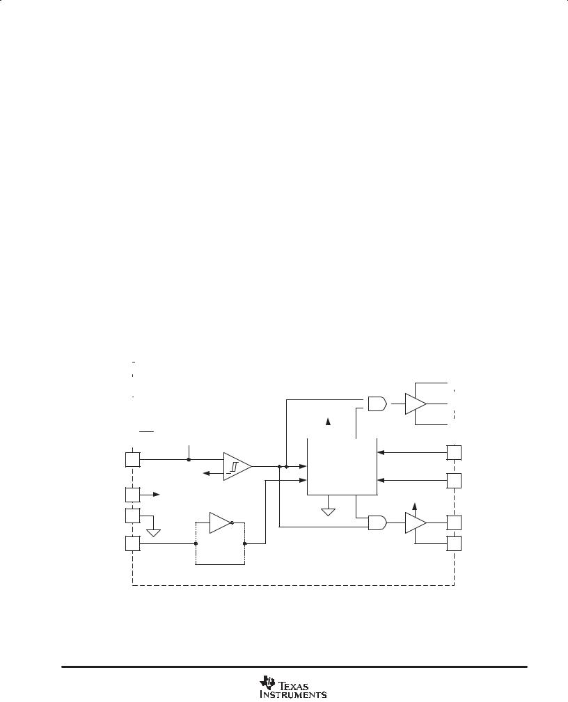
The Predictive Gate Drivet technology utilizes a digital feedback system to detect body-diode conduction, and then adjusts the deadtime delays to minimize it. This system virtually eliminates the body-diode conduction time intervals for the synchronous MOSFET, while adjusting for different MOSFETs characteristics, propagation and load dependent delays. Maximum power stage efficiency is the end result.
Two internal feedback loops in the predictive delay controller continuously adjusts the turn on delays for the two
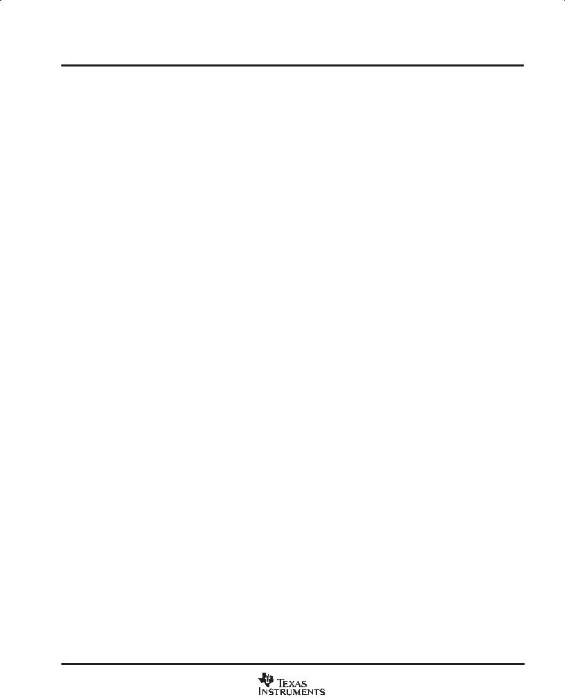
MOSFET gate drives G1 and G2. As shown in Figure 2, tON,G1 and tON,G2 are varied to provide minimum body-diode conduction in the synchronous rectifier MOSFET Q2. The turn-off delay for both G1 and G2, tOFF,G1 and tOFF,G2 are fixed by propagation delays internal to the device.
The predictive delay controller is implemented using a digital control technique, and the time delays are therefore discrete. The turn-on delays, tON, G1 and tON, G2, are changed by a single step (typically 3 ns) every switching cycle. The minimum and maximum turn-on delays for G1 and G2 are specified in the electrical characteristics table.
UCC27221 |
|
3.25 V |
tOFF,G1 |
IN
3.25 V UCC37222
|
|
tOFF,G2 |
|
|
tON,G1 |
|
|
|
|
|
|
|
|
|
|
|
|
|
|
|
|
|
|
tON,G2 |
|
||||||||
|
|
|
|
|
|
|
|
|
|
|
|
|
|
|
|
||||||||||||||||||
|
|
|
|
|
|
|
|
|
|
|
|
|
|
|
|
||||||||||||||||||
|
|
|
|
|
|
|
|
|
|
|
|
|
|
|
|
|
|
|
|
|
|
|
|
|
|
|
|
|
|
|
|
|
|
|
|
|
|
|
|
|
|
|
|
|
|
|
|
|
|
|
|
|
|
|
|
|
|
|
|
|
|
|
|
|
|
|
|
|
|
|
|
|
|
|
|
|
|
|
|
|
|
|
|
|
|
|
|
|
|
|
|
|
|
|
|
|
|
|
|
|
|
|
|
|
|
|
|
|
|
|
|
|
|
|
|
|
|
|
|
|
|
|
|
|
|
|
|
|
|
|
|
|
|
|
|
|
|
|
|
|
|
|
|
|
|
|
|
|
|
|
|
|
|
|
|
|
|
|
|
|
|
|
|
|
|
|
90% |
|
|
|
|
|
|
|
|
|
|
|
|
|
|
|
|
|
|
|
|
|
|
|
|
|
|
|
|
|
|
|
|
|
|
||
|
|
|
|
|
|
|
|
|
|
|
|
|
|
|
|
|
|
|
|
|
|
|
|
|
|
|
|
|
|
|
|||
|
|
|
|
|
|
|
|
|
|
|
|
|
|
|
|
|
|
|
|
|
|
|
|
|
|
|
|
|
|
|
|
|
|
|
|
|
|
|
|
|
|
|
|
|
|
|
|
|
|
|
|
|
|
|
|
|
|
|
|
|
|
|
|
|
|
|
|
G1 |
|
|
|
|
|
|
|
|
|
|
|
|
|
|
10% |
|
|
|
|
|
|
|
|
|
|
|
|
|
|
||||
|
|
|
|
|
|
|
|
|
|
|
|
|
|
|
|
|
|
|
|
|
|
|
|
|
|
|
|
||||||
|
|
|
|
|
|
|
|
|
|
|
|
|
|
|
|
|
|
|
|
|
|
|
|
|
|
|
|
||||||
|
|
|
|
|
|
|
|
|
|
|
|
|
|
|
|
|
|
||||||||||||||||
|
|
|
|
|
|
|
|
|
|
|
|
|
|
|
|
|
|
|
|
|
|||||||||||||
G2
90%
10%
Figure 2. Predictive Gate Drive Timing Diagram
6 |
www.ti.com |
|
|
|
|
UCC27221 |
|
|
|
|
|
UCC27222 |
|
|
|
|
|
SLUS486B − AUGUST 2001 − REVISED JULY 2003 |
|
|
APPLICATION INFORMATION |
|
|||
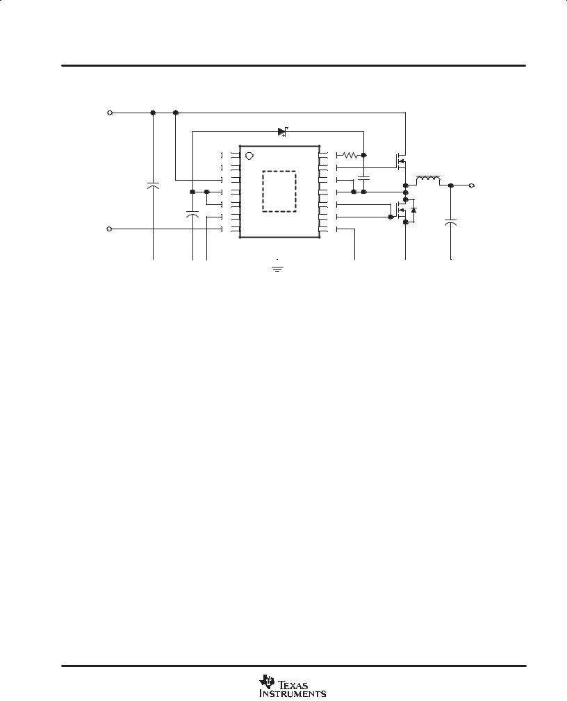
A typical application circuit for systems with 8.5-V to 20-V input is shown in Figure 3. |
|||||
VIN |
|
|
|
|
|
|
|
D1 |
|
|
|
N/C |
UCC27222 |
R1 |
|
||
VHI |
Q1 |
||||
|
|
|
G1 |
||
N/C |
|
|
L1 |
||
CIN |
VDD |
|
SW |
C1 |
|
VLO |
|
SWS |
V OUT |
||
|
|
|
|||
C2 |
PVLO |
|
G2S |
Q2 |
|
AGND |
|
G2 |
|||
|
Cout |
||||
|
|
||||
PWM |
IN |
PGND |
|||
|
|||||
Input |
|
||||
|
|
|
|
||
GND 


 GND
GND
Figure 3. System Application: 8.5-V to 20-V Input
selection of VHI series resistor R1 (dV/dt Considerations):
The series resistor R1 may be needed to slowdown the turn-on of the main forward switch to limit the dV/dt which can inadvertently turn on the synchronous rectifier switch. In nominal 12-V input designs, a R1 value of 4-Ω to 10-Ω can be used depending on the type of MOSFET used and the high-side/low-side MOSFET ratio. In 5-V or lower input applications however, R1 is not needed.
When the drain-source voltage of a MOSFET quickly rises, inadvertent dV/dt induced turn-on of the device is possible. This can especially be a problem for input voltages of 12 V or greater. As Q1 rapidly turns on, the drain-to-source voltage of Q2 rises sharply, resulting in a dV/dt voltage spike appearing on the gate signal of Q2. If the dV/dt induced voltage spike were to exceed the given threshold voltage, the MOSFET may briefly turn on when it should otherwise be commanded off. Obviously this undesired event would have a negative impact on overall efficiency.
Minimizing the dV/dt effect on Q2 can be accomplished by proper MOSFET selection and careful layout techniques. The details of how to select a MOSFET to minimize dV/dt susceptibility are outlined in SEM−1400, Topic 2, Appendix A, Section A5. Secondly, the switch node connecting Q1, Q2 and L1 should be laid out as tight as possible, minimizing any parasitic inductance, which might worsen the dV/dt problem.
If the dV/dt induced voltage spike is still present on the gate Q2, a 4W to 10W value of R1 is recommended to minimize the possibility of inadvertently turning on Q2. The addition of R1 slows the turn-on of Q1, limiting the dV/dt rate appearing on the drain-to-source of Q2. Slowing down the turn-on of Q1 will result in slightly higher switching loss for that device only, but the efficiency gained by preventing dV/dt turn-on of Q2 will far outweigh the negligible effect of adding R1.
When Q2 is optimally selected for dV/dt robustness and careful attention is paid to the PCB layout of the switch node, R1 may not be needed at all, and can therefore be replaced with a 0-Ω jumper to maintain high efficiency. The goal of the designer should not be to completely eliminate the dV/dt turn-on spike but to assure that the maximum amplitude is less than the MOSFET gate-to-source turn-on threshold voltage under all operating conditions.
www.ti.com |
7 |

UCC27221
UCC27222
SLUS486B − AUGUST 2001 − REVISED JULY 2003
APPLICATION INFORMATION
selection of bypass capacitor C1
Bypass capacitors should be selected based upon allowable ripple voltage, usually expressed as a percent of the regulated power supply rail to be bypassed. In all of the UCC27222 application circuits shown herein, C1 provides the bypass for the main (high-side) gate driver. Every time Q1 is switched on, a packet of charge is removed from C1 to charge Q1’s gate to approximately 6.0 V. The charge delivered to the gate of Q1 can be found in the manufacturer’s datasheet curves. An example of a gate charge curve is shown in Figure 4.
GATE-TO-SOURCE VOLTAGE vs
TOTAL GATE CHARGE
|
8 |
|
|
|
|
Voltage − V |
6 |
|
|
|
|
4 |
|
|
|
|
|
Gate-to-Source |
|
|
|
|
|
2 |
|
|
|
|
|
|
|
|
|
|
|
− |
|
|
|
31 nC |
|
GS |
|
|
|
|
|
|
|
|
|
|
|
V |
|
|
|
|
|
|
0 |
|
|
|
|
|
0 |
10 |
20 |
30 |
40 |
|
|
Q6 − Total Gate Charge − nC |
|
||
Figure 4.
As shown in Figure 4, 31 nC of gate charge is required in order for Q1’s gate to be charged to 6.0 V, relative to its source. The minimum bypass capacitor value can be found using the following calculation:
C1MIN |
+ |
|
QG |
|
|
k |
VHI * VSW |
(1) |
|||
|
|
where k is the percent ripple on C1, QG is the total gate charge required to drive the gate of Q1 from zero to the final value of (VHI−VSW). In this example gate charge curve, the value of the quantity (VHI−VSW) is taken to be 6.0 V. This value represents the nominal VLO regulator output voltage minus the forward voltage drop of the external Schottky diode, D1. For the MOSFET with the gate charge described in Figure 4, the minimum capacitance required to maintain a 3% peak-to-peak ripple voltage can be calculated to be 172 nF, so a 180-nF or a 220-nF capacitor could be used. The maximum peak-to-peak C1 ripple must be kept below 0.4 V for proper operation.
8 |
www.ti.com |

UCC27221
UCC27222
SLUS486B − AUGUST 2001 − REVISED JULY 2003
APPLICATION INFORMATION
selection of MOSFETs
The peak current rating of a driver imposes a limit on the maximum gate charge of the external power MOSFET driven by it. The limit is based on the amount of time needed to deliver or remove the required charge to achieve the desired switching speed during turn-on and turn-off of the external transistor. Hence, there are the families of gate driver circuits with different current ratings.
To demonstrate this, assume a constant time interval for the switching transition and a fixed gate drive amplitude. A larger MOSFET with more gate charge will require higher current capability from the driver to turn-on or turn-off the device in the same amount of time. Accordingly, there is a practical upper limit on gate charge which can be driven by the UCC27222 family of drivers. Considering the current capability of the TrueDrive output stage and the available dynamic range (delay adjust range) of the Predictive Gate Drive circuitry, this limit is approximately 120 nC of gate charge.
Some higher current applications require several MOSFETs to be connected parallel and driven by the same gate drive signal. If their combined gate charge exceeds 120 nC, the rise and fall times of the gate drive signals will extend and limit the delay adjust range of the PGD circuit in the UCC27222. This may limit the benefits of the PGD technology under certain operating conditions.
Note that there are additional considerations in the gate drive circuit design which influence the maximum gate charge of the external MOSFETs. The most significant of these is the operating frequency which, together with the amount of gate charge, will define the power dissipation in the driver. The allowable power dissipation is a function of the maximum junction and operating temperatures, thermal and reliability considerations.
selection of bypass capacitor C2
C2 supplies the peak current required to turn on the Q2 synchronous rectifier MOSFET, as well as the peak current to charge the C1 capacitor through the bootstrap diode. Since the synchronous MOSFET is turned on with 0 V across its drain-to-source, there is no Miller, or gate-to-drain charge. Therefore the synchronous MOSFET gate can be modeled as a simple linear capacitance. The value of this capacitance can be found from the datasheet’s gate charge curve. Referring to Figure 5, the slope of the curve past the Miller plateau indicates the equivalent gate capacitance. Because the Y-axis is described in volts, the capacitance is actually the inverse of the slope of the curve. For example, the curve in Figure 4 has a slope of approximately 2 V / 12 nC over the gate charge range of 10 nC to 40 nC. The equivalent capacitance is 12 nC / 2 V = 6 nF. With the equivalent capacitance, the minimum bypass capacitor value can be calculated as:
CEQ |
|
C2MIN + k |
(2) |
where
DCEQ is the equivalent gate capacitance,
Dk is the voltage ripple on C2, expressed as a percentage
For a peak-to-peak ripple of 3%, the minimum C2 capacitor value is calculated to be 200 nF. A 220-nF capacitor would be used in this case.
www.ti.com |
9 |
 Loading...