


Texas Instruments UC3860QTR, UC3860Q, UC3860N, UC3860DWTR, UC3860DW Datasheet
...
UC1860
UC2860
UC3860
Resonant Mode Power Supply Controller
FEATURES
∙3MHz VFO Linear over 100:1 Range
∙5MHz Error Amplifier with Controlled Output Swing
∙Programmable One Shot Timer— Down to 100ns
∙Precision 5V Reference
∙Dual 2A Peak Totem Pole Outputs
∙Programmable Output Sequence
∙Programmable Under Voltage Lockout
∙Very Low Start Up Current
∙Programmable Fault Management & Restart Delay
∙Uncommitted Comparator
DESCRIPTION
The UC1860 family of control ICs is a versatile system for resonant mode power supply control. This device easily implements frequency modulated fixed-on-time control schemes as well as a number of other power supply control schemes with its various dedicated and programmable features.
The UC1860 includes a precision voltage reference, a wide-bandwidth error amplifier, a variable frequency oscillator operable to beyond 3MHz, an oscillator-triggered one-shot, dual high-current totem-pole output drivers, and a programmable toggle flip-flop. The output mode is easily programmed for various sequences such as A, off, B, off; A & B, off; or A, B, off. The error amplifier contains precision output clamps that allow programming of minimum and maximum frequency.
The device also contains an uncommitted comparator, a fast comparator for fault sensing, programmable soft start circuitry, and a programmable restart delay. Hic-up style response to faults is easily achieved. In addition, the UC1860 contains programmable under voltage lockout circuitry that forces the output stages low and minimizes supply current during start-up conditions.
ABSOLUTE MAXIMUM RATINGS
Supply Voltage (pin 19) . . . . . . . . . . . . . . . . . . . . . . . . . . . . 20V Output Current, Source or Sink (pins 17 & 20)
DC . . . . . . . . . . . . . . . . . . . . . . . . . . . . . . . . . . . . . . . . . . 0.8A Pulse (0.5μs) . . . . . . . . . . . . . . . . . . . . . . . . . . . . . . . . . . 3.0A Power Ground Voltage . . . . . . . . . . . . . . . . . . . . . . . . . . . . ±0.2V
Inputs (pins 1, 2, 3, 4, 8, 9, 11, 12,
13, 14, 21, 22, 23 & 24) . . . . . . . . . . . . . . . . . . . . . . -0.4 to 6V Error Amp Output Current, Source or Sink (pin 5) . . . . . . . . 2mA IVFO Current (pin 7). . . . . . . . . . . . . . . . . . . . . . . . . . . . . . . . 2mA Comparator Output Current (pin 15) . . . . . . . . . . . . . . . . . . 5mA
Comparator Output Voltage (pin 15) . . . . . . . . . . . . . . . . . . 15V Soft Start or Restart Delay Sink Current (pins 22 & 23) . . . 5mA Power Dissipation at TA = 50°C (DIP) . . . . . . . . . . . . . . . 1.25W Power Dissipation at TA = 50°C (PLCC) . . . . . . . . . . . . . . . . 1W Lead Temperature (Soldering, 10 seconds) . . . . . . . . . . . 300°C
Note: All voltages are with respect to signal ground and all currents are positive into the specified terminal.
Pin numbers refer to the DIP.
Refer to Packaging Section of Databook for thermal limitations and considerations of packages.
BLOCK DIAGRAM
10/93
UC1860
UC2860
UC3860
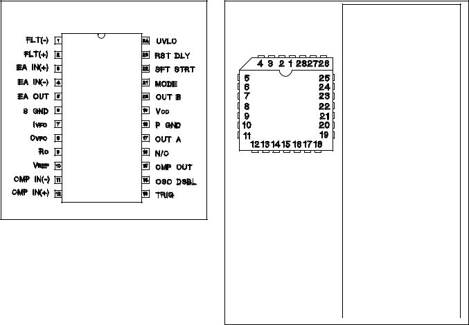
CONNECTION DIAGRAM
DIL - 24 (TOP VIEW) |
J or N Package |
PLCC-28, LCC-28 (TOP VIEW)
Q or L Package
PIN PACKAGE FUNCTION
FUNCTION |
PIN |
S GND |
1 |
IVFO |
2 |
CVFO |
3 |
RC |
4 |
VREF |
5 |
CMP IN (-) |
6 |
CMP IN (+) |
7 |
TRIG |
8 |
OSC DSBL |
9 |
CMP OUT |
10 |
N/C |
11, 12 |
OUT A |
13 |
PGND |
14 |
N/C |
15 |
VCC |
16 |
OUT B |
17 |
N/C |
18, 19 |
MODE |
20 |
SFT STRT |
21 |
RST DLY |
22 |
UVLO |
23 |
FLT (-) |
24 |
FLT (+) |
25 |
EA IN (+) |
26 |
EA IN (-) |
27 |
EA OUT |
28 |
ELECTRICAL CHARACTERISTICS: Unless otherwise stated, all specifications apply for -55°C ≤ TA ≤ 125°C for the UC1860, -25°C ≤ TA ≤ 85°C for the UC2860, 0 ≤ TA ≤ 70°C for the UC3860, VCC = 12V, CVFO = 330pF, IVFO = 0.5mA, C = 330pF, and R = 2.7k, TA = TJ.
PARAMETER |
CONDITIONS |
MIN |
TYP |
MAX |
UNITS |
|
|
|
|
|
|
Reference Section |
|
|
|
|
|
Output Voltage |
TA = 25°C, I O = 0 |
4.95 |
5.00 |
5.05 |
V |
|
IO = 0, Over Temp |
4.93 |
|
5.07 |
V |
Line Regulation |
10 ≤ VCC ≤ 20V |
|
2 |
15 |
mV |
Load Regulation |
0≤ IO ≤ 10mA |
|
2 |
25 |
mV |
Output Noise Voltage* |
10Hz ≤ f ≤ 10kHz |
|
50 |
|
μVRMS |
Short Circuit Current |
VREF = 0V |
-150 |
|
-15 |
mA |
Error Amplifier Section |
|
|
|
|
|
Input Offset Voltage |
2.8 ≤ VCM ≤ 4.5V |
|
1 |
8 |
mV |
Input Bias Current |
|
|
50 |
500 |
nA |
Open Loop Gain |
dVO = 1.5V |
60 |
80 |
|
dB |
PSRR |
10 ≤ VCC ≤ 20V |
70 |
100 |
|
dB |
Output Low (VO-VIVFO) |
-0.1 ≤ IO ≤ 0.1mA |
-8 |
0 |
8 |
mV |
Output High (VO-VIVFO) |
-0.5 ≤ IO ≤ 0.5mA |
1.9 |
2 |
2.1 |
V |
Unity Gain Bandwidth* |
RIN = 2k |
4 |
5 |
|
MHz |
Oscillator Section |
|
|
|
|
|
Nominal Frequency* |
|
1.0 |
1.5 |
2.0 |
MHz |
dF/dIOSC* |
100 ≤ IVFO ≤ 500μA |
2 |
3 |
4 |
GHz/A |
*Guaranteed by design but not 100% tested.
2
UC1860
UC2860
UC3860
ELECTRICAL CHARACTERISTICS: Unless otherwise stated, all specifications apply for -55°C ≤ TA ≤ 125°C for the UC1860, -25° ≤ TA ≤ 85°C for the UC2860, 0 ≤ TA ≤ 70°C for the UC3860, V CC = 12V, CVFO = 330pF, IVFO = 0.5mA, C = 330pF, and R = 2.7k, TA = TJ.
PARAMETER |
CONDITIONS |
MIN |
TYP |
MAX |
UNITS |
|
|
|
|
|
|
Oscillator Section (cont’d) |
|
|
|
|
|
Trig in Threshold |
|
1.0 |
1.4 |
1.8 |
V |
Trig in Open Circuit Voltage |
|
0.7 |
0.9 |
1.1 |
V |
Trig in Delta (VTH-VOC) |
|
0.3 |
0.5 |
0.7 |
V |
Trig in Input Resistance |
dV TRIG = VOC to VTH |
5 |
12 |
25 |
kΩ |
Minimum Trig in Pulse Width* |
|
|
3 |
10 |
ns |
Osc. Disable Threshold |
|
1.0 |
1.4 |
1.8 |
V |
One Shot Timer |
|
|
|
|
|
On Time* |
|
150 |
200 |
250 |
ns |
Clamp Frequency* |
IVFO = 1.5mA |
2.8 |
3.7 |
4.6 |
MHz |
Dead Time* |
IVFO =1.5mA |
35 |
70 |
100 |
ns |
Output Stage |
|
|
|
|
|
Output Low Saturation |
20mA |
|
0.2 |
0.4 |
V |
|
200mA |
|
0.5 |
2.2 |
V |
Output High Saturation |
-20mA |
|
1.5 |
2.0 |
V |
|
-200mA |
|
1.7 |
2.5 |
V |
Rise/Fall Time* |
CLOAD = 1nF |
|
15 |
30 |
ns |
UVLO Low Saturation |
20mA |
|
0.8 |
1.5 |
V |
Output Mode Low Input |
|
|
|
0.4 |
V |
Output Mode High Input |
|
2.0 |
|
|
V |
Under Voltage Lockout Section |
|
|
|
|
|
VCC Comparator Threshold |
On |
16 |
17.3 |
18.5 |
V |
|
Off |
9.5 |
10.5 |
12 |
V |
UVLO Comparator Threshold |
On |
3.6 |
4.2 |
4.8 |
V |
|
Hysteresis |
0.2 |
0.4 |
0.6 |
V |
UVLO Input Resistance |
UVLO = 4/VCC = 8 |
10 |
23 |
50 |
kΩ |
VREF Comparator Threshold |
VCC = UVLO = VREF |
|
4.5 |
4.9 |
V |
Supply Current |
|
|
|
|
|
ICC |
VCC = 12V, VOSC DSBL = 3V |
|
30 |
40 |
mA |
ISTART |
UVLO pin open |
|
0.3 |
0.5 |
mA |
|
VCC = VCC (on) -0.3V |
|
|
|
|
Fault Comparator |
|
|
|
|
|
Input Offset Voltage |
−0.3 ≤ VCM ≤ 3V |
|
2 |
10 |
mV |
Input Bias Current |
VCM = 0V |
|
100 |
200 |
μA |
Input Offset Current |
VCM = 0V |
|
10 |
30 |
μA |
Propagation Delay To Output* |
±50mV input |
|
100 |
150 |
ns |
Uncommitted Comparator |
|
|
|
|
|
Input Offset Voltage |
-0.3 ≤ VCM ≤ 3V |
|
2 |
10 |
mV |
Input Bias Current |
VCM = 0V |
|
100 |
200 |
μA |
Input Offset Current |
VCM = 0V |
|
10 |
30 |
μA |
Output Low Voltage |
IO = 2mA |
|
0.3 |
0.5 |
V |
Propagation Delay To Sat* |
±50mV input, 2.5k load to 5V |
|
50 |
100 |
ns |
Soft Start/Restart Control Section |
|
|
|
|
|
Saturation Voltage (2 pins) |
ISINK = 100μA |
|
0.2 |
0.5 |
V |
Charge Current (2 pins) |
|
2 |
5 |
10 |
μA |
Restart Delay Threshold |
|
2.8 |
3.0 |
3.2 |
V |
*Guaranteed by design but not 100% tested.
3
 Loading...