


UCC28083, UCC28084, UCC28085, UCC28086
UCC38083, UCC38084, UCC38085, UCC38086
SLUS488D -- SEPTEMBER 2002 -- REVISED AUGUST 2006
8-PIN CURRENT MODE PUSH-PULL PWM CONTROLLERS WITH PROGRAMMABLE SLOPE COMPENSATION
FEATURES
D Programmable Slope Compensation D Internal Soft-Start on the UCC38083/4 D Cycle-by-Cycle Current Limiting
DLow Start-Up Current of 120 μA and 1.5 mA
Typical Run Current
DSingle External Component Oscillator Programmable from 50 kHz to 1 MHz
APPLICATIONS
D High-Efficiency Switch-Mode Power Supplies D Telecom dc-to-dc Converters
D Point-of-Load or Point-of-Use Power Modules
DLow-Cost Push-Pull and Half-Bridge Applications
DESCRIPTION
DHigh-Current Totem-Pole Dual Output Stage Drives Push-Pull Configuration with 1-A Sink and 0.5-A Source Capability
DCurrent Sense Discharge Transistor to Improve Dynamic Response
D Internally Trimmed Bandgap Reference D Undervoltage Lockout with Hysteresis
BASIC APPLICATION
VIN |
POWER |
VOUT |
|
||
|
TRANSFORMER |
|
|
|
VDD
UCC3808x
CTRL |
OUTA |
|
RT |
OUTB |
|
|
RF |
|
ISET |
CS |
|
GND |
|
|
RT |
|
RS |
RSET |
CF |
|
FEEDBACK
The UCC38083/4/5/6 is a family of BiCMOS pulse width modulation (PWM) controllers for dc-to-dc or off-line fixed-frequency current-mode switching power supplies. The dual output stages are configured for the push-pull topology. Both outputs switch at half the oscillator frequency using a toggle flip-flop. The dead time between the two outputs is typically 110 ns, limiting each output’s duty cycle to less than 50%.
The new UCC3808x family is based on the UCC3808A architecture. The major differences include the addition of a programmable slope compensation ramp to the CS signal and the removal of the error amplifier. The current flowing out of the ISET pin through an external resistor is monitored internally to set the magnitude of the slope compensation function. This device also includes an internal discharge transistor from the CS pin to ground, which is activated at each clock cycle after the pulse is terminated. This discharges any filter capacitance on the CS pin during each cycle and helps minimize filter capacitor values and current sense delay.
The UCC38083 and the UCC38084 devices have a typical soft-start interval time of 3.5 ms while the UCC38085 and the UCC38086 has less than 100 μs for applications where internal soft-start is not desired.
The UCC38083 and the UCC38085 devices have the turn-on/off thresholds of 12.5 V / 8.3 V, while the UCC38084 and the UCC38086 has the turn-on/off thresholds of 4.3 V / 4.1 V. Each device is offered in 8-pin TSSOP (PW), 8-pin SOIC (D) and 8-pin PDIP (P) packages.
UDG--01080
Please be aware that an important notice concerning availability, standard warranty, and use in critical applications of Texas Instruments semiconductor products and disclaimers thereto appears at the end of this data sheet.
|
|
|
PRODUCTION DATA information is current as of publication date. |
Copyright © 2002--2006, Texas Instruments Incorporated |
|
Products conform to specifications per the terms of Texas Instruments |
|
|
standard warranty. Production processing does not necessarily include |
|
|
testing of all parameters. |
|
|
www.ti.com |
1 |

UCC28083, UCC28084, UCC28085, UCC28086
UCC38083, UCC38084, UCC38085, UCC38086
SLUS488D -- SEPTEMBER 2002 -- REVISED AUGUST 2006
ORDERING INFORMATION
THERMAL RESISTANCE TABLE
PACKAGE |
θjc(°C/W) |
θja(°C/W) |
|
|
|
|
|
SOIC--8 |
(D) |
42 |
84 to 160(1) |
PDIP--8 |
(P) |
50 |
110(1) |
TSSOP--8 |
(PW) |
32(2) |
232 to 257(2) |
NOTES: (1) Specified θja (junction to ambient) is for devices mounted to 5-inch2 FR4 PC board with one ounce copper where noted. When resistance range is given, lower values are for 5 inch2 aluminum PC board. Test PWB was 0.062 inch thick and typically used 0.635-mm trace widths for power packages and 1.3-mm trace widths for non-power packages with a 100-mil x 100-mil probe land area at the end of each trace.
(2). Modeled data. If value range given for θja, lower value is for 3x3 inch. 1 oz internal copper ground plane, higher value is for 1x1-inch. ground plane. All model data assumes only one trace for each non-fused lead.
AVAILABLE OPTIONS
TA |
INTERNAL |
UVLO |
|
PACKAGES |
|
|||
|
|
|
|
|
||||
SOFT START |
ON |
OFF |
SOIC-8 (D) |
PDIP-8 (P) |
TSSOP-8 (PW) |
|||
|
||||||||
|
|
|
|
|
|
|
|
|
|
3.5 ms |
12.5 V |
8.3 V |
UCC28083D |
UCC28083P |
UCC28083PW |
||
|
|
|
|
|
|
|||
--40°C to 85°C |
4.3 V |
4.1 V |
UCC28084D |
UCC28084P |
UCC28084PW |
|||
|
|
|||||||
|
|
|
|
|
|
|
||
75 |
μs |
12.5 V |
8.3 V |
UCC28085D |
UCC28085P |
UCC28085PW |
||
|
||||||||
|
|
|
|
|
|
|||
|
4.3 V |
4.1 V |
UCC28086D |
UCC28086P |
UCC28086PW |
|||
|
|
|
||||||
|
|
|
|
|
|
|
|
|
|
3.5 ms |
12.5 V |
8.3 V |
UCC38083D |
UCC38083P |
UCC38083PW |
||
|
|
|
|
|
|
|||
0°C to 70°C |
4.3 V |
4.1 V |
UCC38084D |
UCC38084P |
UCC38084PW |
|||
|
|
|||||||
|
|
|
|
|
|
|
||
75 |
μs |
12.5 V |
8.3 V |
UCC38085D |
UCC38085P |
UCC38085PW |
||
|
||||||||
|
|
|
|
|
|
|||
|
4.3 V |
4.1 V |
UCC38086D |
UCC38086P |
UCC38086PW |
|||
|
|
|
||||||
|
|
|
|
|
|
|
|
|
†The D and PW packages are available taped and reeled. Add R suffix to device type, e.g. UCC28083DR (2500 devices per reel) or UCC38083PWR (2000 devices per reel).
D OR P PACKAGE |
|
|
PW PACKAGE |
|
||||
|
(TOP VIEW) |
|
|
|
(TOP VIEW) |
|
||
CTRL |
1 |
8 |
VDD |
OUTA |
1 |
8 |
OUTB |
|
ISET |
2 |
7 |
OUTA |
VDD |
2 |
7 |
GND |
|
CTRL |
3 |
6 |
RT |
|||||
CS |
3 |
6 |
OUTB |
|||||
ISET |
4 |
5 |
CS |
|||||
RT |
4 |
5 |
GND |
|||||
|
|
|
|
|||||
2 |
www.ti.com |

|
|
|
UCC28083, UCC28084, UCC28085, UCC28086 |
|
|
|
UCC38083, UCC38084, UCC38085, UCC38086 |
|
|
|
SLUS488D -- SEPTEMBER 2002 -- REVISED AUGUST 2006 |
|
|||
absolute maximum ratings over operating free-air temperature (unless otherwise noted)† |
|||
Supply voltage, VDD (IDD < 10 mA) . . . . . . . . . . . . . . . . . . . |
. . . . . . . . . . . . . . . . . . . . . . . . . . . . . . . . . . . . . . . . . . 15 V |
||
Supply current, IDD . . . |
. . . . . . . . |
. . . . . . . . . . . . . . . . . . . . . . |
. . . . . . . . . . . . . . . . . . . . . . . . . . . . . . . . . . . . . . . . 20 mA |
Sink current (peak): |
OUTA . . |
. . . . . . . . . . . . . . . . . . . . . |
. . . . . . . . . . . . . . . . . . . . . . . . . . . . . . . . . . . . . . . . . 1.0 A |
|
OUTB . . |
. . . . . . . . . . . . . . . . . . . . . |
. . . . . . . . . . . . . . . . . . . . . . . . . . . . . . . . . . . . . . . . . 1.0 A |
Source current (peak): |
OUTA . . |
. . . . . . . . . . . . . . . . . . . . . |
. . . . . . . . . . . . . . . . . . . . . . . . . . . . . . . . . . . . . . . . --0.5 A |
|
OUTB . . |
. . . . . . . . . . . . . . . . . . . . . |
. . . . . . . . . . . . . . . . . . . . . . . . . . . . . . . . . . . . . . . . --0.5 A |
Analog inputs: |
CTRL . . |
. . . . . . . . . . . . . . . . . . . . . |
. . . . . . . . . . . . . . . . . . . . . . . . . . . --0.3 V to VDD +0.3 V |
|
CS . . . . . |
. . . . . . . . . . . . . . . . . . . . . |
. . . . . . . . . . . --0.3 V to VDD +0.3 V, not to exceed 6 V |
|
RSET (minimum) . . . . . . . . . . . . . . |
. . . . . . . . . . . . . . . . . . . . . . . . . . . . . . . . . . . . . . . . >5 kΩ |
|
|
RT (--100 μA < IRT < 100 μA) . . . . |
. . . . . . . . . . . . . . . . . . . . . . . . . . . . . . . . . --0.3 V to 2.0 V |
|
Power dissipation at TA = 25°C |
(P package) . . . . . . . . . . |
. . . . . . . . . . . . . . . . . . . . . . . . . . . . . . . . . . . . . . . . . . 1 W |
|
Power dissipation at TA = 25°C |
(D package) . . . . . . . . . . |
. . . . . . . . . . . . . . . . . . . . . . . . . . . . . . . . . . . . . . 650 mW |
|
Power dissipation at TA = 25°C |
(PW package) . . . . . . . . |
. . . . . . . . . . . . . . . . . . . . . . . . . . . . . . . . . . . . . . 400 mW |
|
Junction operating temperature, TJ . . . . . . . . . . . . . . . . . . . |
. . . . . . . . . . . . . . . . . . . . . . . . . . . . . . . . --55°C to 150°C |
||
Storage temperature, Tstg . . . . . . . |
. . . . . . . . . . . . . . . . . . . . . |
. . . . . . . . . . . . . . . . . . . . . . . . . . . . . . . . --65°C to 150°C |
|
Lead temperature (soldering 10 seconds) . . . . . . . . . . . . . . |
. . . . . . . . . . . . . . . . . . . . . . . . . . . . . . . . . . . . . . . . 300°C |
||
†Stresses beyond those listed under “absolute maximum ratings” may cause permanent damage to the device. These are stress ratings only, and functional operation of the device at these or any other conditions beyond those indicated under “recommended operating conditions” is not implied. Exposure to absolute-maximum-rated conditions for extended periods may affect device reliability. All voltages are with respect to GND. Currents are positive into, and negative out of the specified terminal.
electrical characteristics over recommended operating virtual junction temperature range, VDD = 10 V (See Note 1),1-μF capacitor from VDD to GND, RT = 165 kΩ, RF = 1 kΩ, CF = 220 pF,
RSET = 50 kΩ, TA = --40°C to 85°C for UCC2808x, TA = 0°C to 70°C for UCC3808x, TA = TJ
(unless otherwise noted) overall
PARAMETER |
|
TEST CONDITIONS |
MIN |
TYP |
MAX |
UNITS |
|
|
|
|
|
|
|
Start-up current |
VDD < UVLO start threshold voltage |
|
120 |
200 |
μA |
|
|
|
|
|
|
|
|
Supply current |
CTRL = 0 V, |
CS = 0 V, |
|
1.5 |
2.5 |
mA |
|
See Note 1 |
|
|
|
|
|
|
|
|
|
|
|
|
undervoltage lockout
PARAMETER |
|
TEST CONDITIONS |
MIN |
TYP |
MAX |
UNITS |
|
|
|
|
|
|
|
Start threshold voltage |
UCC38083/5 |
See Note 1 |
11.5 |
12.5 |
13.5 |
|
|
|
|
|
|
|
|
UCC38084/6 |
|
4.1 |
4.3 |
4.5 |
|
|
|
|
|
||||
|
|
|
|
|
|
|
Minimum operating voltage |
UCC38083/5 |
|
7.6 |
8.3 |
9.0 |
V |
|
|
|
|
|
||
after start |
UCC38084/6 |
|
3.9 |
4.1 |
4.3 |
|
|
|
|||||
|
|
|
|
|
|
|
Hysteresis voltage |
UCC38083/5 |
|
3.5 |
4.2 |
5.1 |
|
|
|
|
|
|
|
|
UCC38084/6 |
|
0.1 |
0.2 |
0.3 |
|
|
|
|
|
||||
|
|
|
|
|
|
|
oscillator
PARAMETER |
|
TEST CONDITIONS |
MIN |
TYP |
MAX |
UNITS |
|
|
|
|
|
|
|
Frequency |
2 x f(OUTA) |
|
180 |
200 |
220 |
kHz |
|
|
|
|
|
|
|
Voltage amplitude |
See Note 2 |
|
1.4 |
1.5 |
1.6 |
V |
|
|
|
|
|
|
|
Oscillator fall time (dead time) |
|
|
|
110 |
220 |
ns |
|
|
|
|
|
|
|
RT pin voltage |
|
|
1.2 |
1.5 |
1.6 |
V |
|
|
|
|
|
|
|
|
|
|
|
|
|
|
www.ti.com |
3 |

UCC28083, UCC28084, UCC28085, UCC28086
UCC38083, UCC38084, UCC38085, UCC38086
SLUS488D -- SEPTEMBER 2002 -- REVISED AUGUST 2006
electrical characteristics over recommended operating virtual junction temperature range, VDD = 10 V (See Note 1),1-μF capacitor from VDD to GND, RT = 165 kΩ, RF = 1 kΩ, CF = 220 pF,
RSET = 50 kΩ, TA = --40°C to 85°C for UCC2808x, TA = 0°C to 70°C for UCC3808x, TA = TJ
(unless otherwise noted) current sense
PARAMETER |
|
TEST CONDITIONS |
MIN |
TYP |
MAX |
UNITS |
|
|
|
|
|
|
|
Gain |
See Note 3 |
|
1.9 |
2.2 |
2.5 |
V/V |
|
|
|
|
|
|
|
Maximum input signal voltage |
CTRL = 5 V, |
See Note 4 |
0.47 |
0.52 |
0.57 |
V |
|
|
|
|
|
|
|
CS to output delay time |
CTRL = 3.5 V, |
0 mV ≤ CS ≤ 600 mV |
|
100 |
200 |
ns |
|
|
|
|
|
|
|
Source current |
|
|
--200 |
|
|
nA |
|
|
|
|
|
|
|
Sink current |
CS = 0.5 V, |
RT = 2.0 V, |
3 |
7 |
12 |
mA |
See Note 5 |
|
|||||
|
|
|
|
|
|
|
|
|
|
|
|
|
|
Overcurrent threshold voltage |
|
|
0.70 |
0.75 |
0.80 |
V |
|
|
|
|
|
|
|
CTRL to CS offset voltage |
CS = 0 V, 25°C |
0.55 |
0.70 |
0.90 |
V |
|
|
|
|
|
|
|
|
CS = 0 V |
|
0.37 |
0.70 |
1.10 |
V |
|
|
|
|||||
|
|
|
|
|
|
|
pulse width modulation
PARAMETER |
TEST CONDITIONS |
MIN |
TYP |
MAX |
UNITS |
|
|
|
|
|
|
Maximum duty cycle |
Measured at OUTA or OUTB, See Note 7 |
48% |
49% |
50% |
|
|
|
|
|
|
|
Minimum duty cycle |
CTRL = 0 V |
|
|
0% |
|
|
|
|
|
|
|
output
PARAMETER |
TEST CONDITIONS |
MIN |
TYP |
MAX |
UNITS |
|
|
|
|
|
|
|
|
Low-level output voltage (OUTA or OUTB) |
IOUT = 100 mA |
|
|
0.5 |
1.0 |
V |
High-level output voltage (OUTA or OUTB) |
IOUT = --50 mA, |
(VDD -- VOUT), See Note 6 |
|
0.5 |
1.0 |
|
|
|
|||||
Rise time |
CLOAD = 1 nF |
|
|
25 |
60 |
ns |
Fall time |
CLOAD = 1 nF |
|
|
25 |
60 |
|
|
|
|
||||
soft-start
PARAMETER |
|
TEST CONDITIONS |
MIN |
TYP |
MAX |
UNITS |
|
|
|
|
|
|
|
|
|
OUTA/OUTB soft-start interval time, |
CTRL = 1.8 V, |
CS = 0 V, |
1.3 |
3.5 |
8.5 |
ms |
|
UCC38083/4 |
Duty cycle from 0 to full, See Note 8 |
||||||
|
|
|
|
||||
|
|
|
|
|
|
|
|
OUTA/OUTB soft-start interval time, |
CTRL = 1.8 V, |
CS = 0 V, |
30 |
75 |
110 |
μs |
|
UCC38085/6 |
Duty cycle from 0 to full, See Note 8 |
||||||
|
|
|
|
||||
|
|
|
|
|
|
|
|
slope compensation
PARAMETER |
|
|
|
TEST CONDITIONS |
MIN |
TYP |
MAX |
UNITS |
|
|
|
|
|
|
|
|
|
IRAMP, peak |
|
|
|
ISET, peak = 30 μA, Full duty cycle |
125 |
150 |
175 |
μA |
NOTE 1: For UCCx8083/5, set VDD above the start threshold before setting to 10 V. |
|
|
|
|
||||
NOTE 2: Measured at ISET pin. |
|
|
|
|
|
|
|
|
NOTE 3: Gain is defined by A = |
VCTRL |
, 0 ≤ VCS ≤ 0.4 V. |
|
|
|
|
||
V |
CS |
|
|
|
|
|||
NOTE 4: Measured at trip point of latch with CS ramped from 0.4 V to 0.6 V.
NOTE 5: This internal current sink on the CS pin is designed to discharge and external filter capacitor. It is not intended to be a dc sink path. NOTE 6: Not 100% production tested. Ensured by design and also by the rise time test.
NOTE 7: For devices in PW package, parameter tested at wafer probe. NOTE 8: Ensured by design.
4 |
www.ti.com |

UCC28083, UCC28084, UCC28085, UCC28086
UCC38083, UCC38084, UCC38085, UCC38086
SLUS488D -- SEPTEMBER 2002 -- REVISED AUGUST 2006
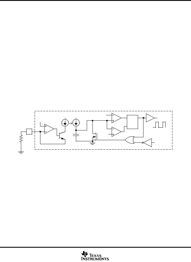
functional block diagram
|
|
|
|
|
Soft Start and Fault Latch |
|
Bias/UVLO |
|
CTRL |
1 |
|
|
Iss |
|
S |
Q |
VREF |
|
|
|
|
|
|
|
|
|
|
|
|
|
0.5V |
|
|
|
|
|
|
Slope Circuit |
ISLOPE |
|
R |
|
8 |
|
|
|
|
|
|
|
|||
|
|
|
|
Vdd--1 |
|
|
|
VDD |
|
|
|
|
|
|
S |
Q |
|
|
|
|
|
|
|
+ |
||
|
|
|
|
|
|
|
|
|
|
|
CT |
|
|
|
R |
|
|
|
|
|
|
Css |
|
|
|
|
|
|
|
|
|
|
|
|
|
ISET |
2 |
|
ISLOPE = |
|
|
|
|
|
|
5 x I SET |
|
|
|
|
|
||
|
|
CS Circuitry |
|
PWM Comparator/Latch |
|
|
Output Driver |
|
|
|
0.75V |
|
|
|
|
|
7 |
|
|
|
|
|
|
|
|
|
|
|
|
|
80 kΩ |
S |
Q |
|
OUTA |
|
|
|
|
|
|
Q |
||
|
|
|
|
|
|
|
|
|
|
|
0.5V |
|
60 kΩ |
R |
|
|
T |
|
|
|
0.3 V |
|
|
Q |
||
|
|
|
|
|
|
|
||
|
|
|
|
|
|
|
|
|
CS |
3 |
|
|
|
|
|
|
6 |
|
|
|
|
|
|
|
|
|
|
|
|
|
|
|
|
|
OUTB |
|
|
|
|
Oscillator |
|
|
|
|
|
|
|
|
1.5V |
S Q |
|
|
|
|
|
1.5V |
|
ICT |
|
|
|
|
|
|
|
|
|
|
|
||
|
|
|
|
|
|
|
|
|
|
|
|
|
|
R |
|
|
|
RT |
4 |
|
|
0.2V |
|
|
|
5 |
|
|
|
|
|
|
|
|
|
|
|
|
|
CT |
|
|
|
GND |
|
|
|
|
|
|
|
|
|
|
|
|
|
|
|
|
|
UDG--01081 |
|
|
|
|
Terminal Functions |
|
|
||
|
TERMINAL |
|
|
|
|
|
|
|
NAME |
PACKAGE |
I/O |
|
|
DESCRIPTION |
|
||
|
|
D OR P |
|
|
|
|
|
|
CS |
|
3 |
I |
The current-sense input to the PWM comparator, the cycle-by-cycle peak current comparator, and the |
||||
|
|
|
|
overcurrent comparator. The overcurrent comparator is only intended for fault sensing. Exceeding the |
||||
|
|
|
|
overcurrent threshold causes a soft-start cycle. An internal MOSFET discharges the current-sense filter |
||||
|
|
|
|
capacitor to improve dynamic performance of the power converter. |
|
|||
CTRL |
1 |
I |
Error voltage input to PWM comparator. |
|
|
|
||
GND |
5 |
-- |
Reference ground and power ground for all functions. Due to high currents, and high-frequency operation |
|||||
|
|
|
|
of the IC, a low-impedance circuit board ground plane is highly recommended. |
||||
ISET |
2 |
I |
Current selection for slope compensation. |
|
|
|||
OUTA |
7 |
O |
Alternating high-current output stages. |
|
|
|
||
OUTB |
6 |
O |
|
|
|
|||
|
|
|
|
|
||||
RT |
|
4 |
I |
Programs the oscillator. |
|
|
|
|
VDD |
|
8 |
I |
Power input connection. |
|
|
|
|
www.ti.com |
5 |

UCC28083, UCC28084, UCC28085, UCC28086
UCC38083, UCC38084, UCC38085, UCC38086
SLUS488D -- SEPTEMBER 2002 -- REVISED AUGUST 2006
detailed pin descriptions
CTRL: The error voltage is typically generated by a secondary-side error amplifier and transmitted to the primary-side referenced UCC3808x by means of an opto-coupler. CTRL has an internal divider ratio of 0.45 to maintain a usable range with the minimum VDD of 4.1 V. The UCC38083/UCC38084 family features a built-in full-cycle soft start while the UCC38085/6 does not.
For the UCC38083/4, soft-start is implemented as a clamp at the input to the PWM comparator. This causes the output pulses to start near 0% duty cycle and increase until the clamp exceeds the CTRL voltage.
ISET: Program the slope compensation current ramp by connecting a resistor, RSET, from ISET to ground. The voltage of the ISET pin tracks the 1.5-V internal oscillator ramp, as shown in Figure 1.
|
V(CS) |
|
VDD |
|
|
|
10k |
|
|
UCC38083 |
|
ISET |
RSET |
1 CTRL |
VDD 8 |
|
|
|
|
2 ISET OUTA 7
|
|
|
CS |
OUTB |
1uF |
|
|
|
3 |
6 |
|||
|
RF |
4 |
RT |
GND |
5 |
|
IRAMP |
1k |
|||||
|
|
|
|
|||
|
220pF |
RT |
|
|
|
|
|
165k |
|
|
|
||
|
|
|
|
|
 IRAMP, peak = 5 x ISET, peak
IRAMP
ISET
OUTA
OUTB
Figure 1. Full Duty Cycle Output
The compensating current source, ISLOPE, at the CS pin is proportional to the ISET current, according to the relation:
ISLOPE = 5 × ISET |
(1) |
The ramping current due to ISLOPE develops a voltage across the effective filter impedance that is normally connected from the current sense resistor to the CS input. In order to program a desired compensating slope with a specific peak compensating ramp voltage at the CS pin, use the RSET value in the following equation:
5 × RF |
|
RSET = VOSC(peak) × RAMP VOLTAGE HEIGHT |
(2) |
Where VOSC(peak) = 1.5 V
Notice that the PWM Latch drives an internal MOSFET that will discharge an external filtering capacitor on the
CS pin. Thus, ISLOPE will appear to terminate when the PWM comparator or the cycle-by-cycle current limit comparator sets the PWM latch. The actual compensating slope is not affected by premature termination of the
switching cycle.
6 |
www.ti.com |
UCC28083, UCC28084, UCC28085, UCC28086
UCC38083, UCC38084, UCC38085, UCC38086
SLUS488D -- SEPTEMBER 2002 -- REVISED AUGUST 2006
detailed pin descriptions (continued)
OUTA and OUTB: Alternating high-current output stages. Both stages are capable of driving the gate of a power MOSFET. Each stage is capable of 500-mA peak-source current, and 1-A peak-sink current.
The output stages switch at half the oscillator frequency, in a push-pull configuration. When the voltage on the internal oscillator capacitor is rising, one of the two outputs is high, but during fall time, both outputs are off. This dead time between the two outputs, along with a slower output rise time than fall time, ensures that the two outputs cannot be on at the same time. This dead time is typically 110 ns.
The high-current output drivers consist of MOSFET output devices, which switch from VDD to GND. Each output stage also provides a very low impedance to overshoot and undershoot. This means that in many cases, external Schottky clamp diodes are not required.
RT: The oscillator programming pin. The oscillator features an internal timing capacitor. An external resistor, RT, sets a current from the RT pin to ground. Due to variations in the internal CT, nominal VRT of 1.5 V can vary from 1.2 V to 1.6 V
Selecting RT as shown programs the oscillator frequency:
|
1 |
1 |
|
--7 |
|
|
||
RT = |
|
|
|
|
−2.0 × 10 |
|
|
|
28.7 × |
10--12 |
fOSC |
|
(3) |
||||
where fOSC is in Hz, resistance in Ω. The recommended range of timing resistors is between 25 kΩand 698 kΩ. For best performance, keep the timing resistor lead from the RT pin to GND (pin 5) as short as possible.
|
|
1.5 V |
|
|
IRT |
S |
Q |
1.5 V |
ICT |
|
|
|
|
R |
|
4 |
|
0.2 V |
OSCILLATOR |
|
|
OUTPUT |
|
|
|
C T |
|
R T |
|
|
|
Approximate Frequency |
= |
1 |
|
28.7 ×10--12 × RT + 2.0 × 10--7 |
|
||
|
|
|
UDG--01083 |
Figure 2. Block Diagram for Oscillator |
|||
VDD: The power input connection for this device. Although quiescent VDD current is very low, total supply current may be higher, depending on OUTA and OUTB current, and the programmed oscillator frequency. Total VDD current is the sum of quiescent VDD current and the average OUT current. Knowing the operating frequency and the MOSFET gate charge (QG), average OUT current can be calculated from:
IOUT = QG ×fOSC |
(4) |
where f is the oscillator frequency.
To prevent noise problems, bypass VDD to GND with a ceramic capacitor as close to the chip as possible along with an electrolytic capacitor. A 1-μF decoupling capacitor is recommended.
www.ti.com |
7 |
UCC28083, UCC28084, UCC28085, UCC28086
UCC38083, UCC38084, UCC38085, UCC38086
SLUS488D -- SEPTEMBER 2002 -- REVISED AUGUST 2006
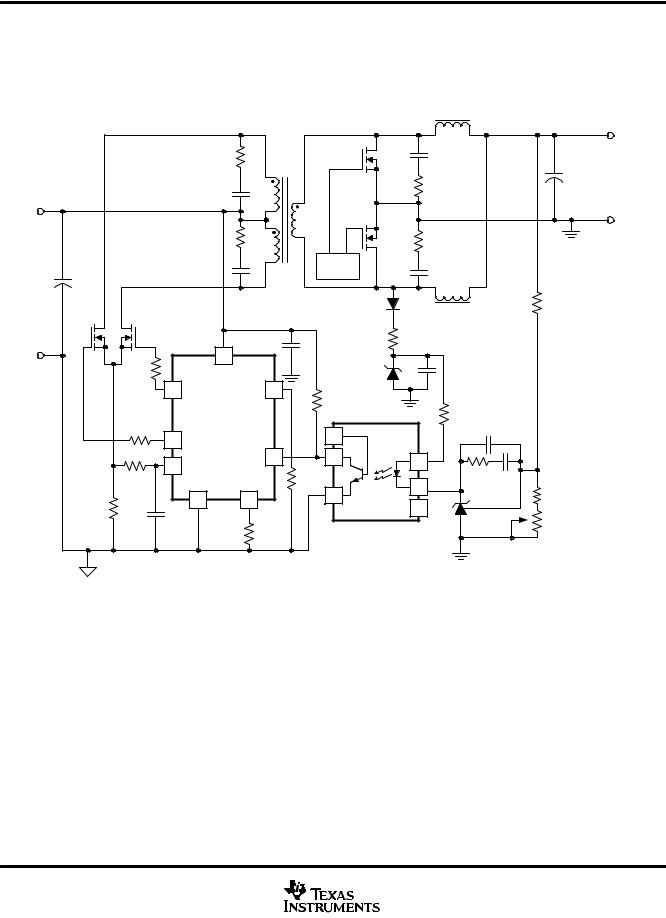
APPLICATION INFORMATION
The following application circuit shows an isolated 12-VIN to 2.5 VOUT push-pull converter with scalable output power (20 W to 200 W). Note that the pinout shown is for SOIC-8 and PDIP-8 packages.
typical application
VIN = 12 V +/-20%V
SR
DRIVE
|
|
|
1 μF |
|
|
|
|
|
|
8 |
|
|
|
4.7Ω |
|
VDD |
|
|
|
|
7 |
OUTA |
RT |
4 |
|
|
|
|
|
|
||||
4.7Ω |
|
UCC3808x |
|
|
|
|
6 |
OUTB |
|
|
6 |
|
|
|
|
|
|
|||
|
|
|
|
|
||
RF 1 kΩ |
3 |
CS |
CTRL |
1 |
5 |
1 |
|
|
|
|
|||
|
|
|
|
|
||
|
|
GND |
ISET |
165 |
|
2 |
|
|
kΩ |
|
|||
|
|
|
|
4 |
||
RS |
|
5 |
2 |
|
||
|
|
|
3 |
|||
CF |
|
|
|
|
||
|
|
|
|
|
TL431 |
|
|
220 pF |
RSET |
|
|
||
|
|
|
|
|
||
VO= 2.2 V TO 3.3 V ADJUSTABLE
UDG--01084
8 |
www.ti.com |

UCC28083, UCC28084, UCC28085, UCC28086
UCC38083, UCC38084, UCC38085, UCC38086
SLUS488D -- SEPTEMBER 2002 -- REVISED AUGUST 2006
APPLICATION INFORMATION
operational waveforms
Figure 3 illustrates how the voltage ramp is effectively added to the voltage across the current sense element VCS, to implement slope compensation.
OUTA
OUTB
VRS
ADDED
RAMP
VOLTAGE
VCS, Pin 3
UDG--01085
Figure 3. Typical Slope Compensation Waveforms at 80% Duty Cycle
In Figure 3, OUTA and OUTB are shown at a duty cycle of 80%, with the associated voltage VRS across the current sense resistor of the primary push-pull power MOSFETs. The current flowing out of CS generates the ramp voltage across the filter resistor RF that is positioned between the power current sense resistor and the CS pin. This voltage is effectively added to VRS to provide slope compensation at VCS, pin 3. A capacitor CF is also recommended to filter the waveform at CS.
www.ti.com |
9 |
 Loading...