


Texas Instruments UC3834Q, UC3834QTR, UC3834N, UC3834J, UC3834DWTR Datasheet
...
UC1834
UC2834
UC3834
High Efficiency Linear Regulator
FEATURES
∙Minimum VIN - VOUT Less Than 0.5V At 5A Load With External Pass Device
∙Equally Usable For Either Positive or Negative Regulator Design
∙Adjustable Low Threshold Current Sense Amplifier
∙Under And Over-Voltage Fault Alert With Programmable Delay
∙Over-Voltage Fault Latch With 100mA Crowbar Drive Output
DESCRIPTION
The UC1834 family of integrated circuits is optimized for the design of low input-output differential linear regulators. A high gain amplifier and 200mA sink or source drive outputs facilitate high output current designs which use an external pass device. With both positive and negative precision references, either polarity of regulator can be implemented. A current sense amplifier with a low, adjustable, threshold can be used to sense and limit currents in either the positive or negative supply lines.
In addition, this series of parts has a fault monitoring circuit which senses both under and over-voltage fault conditions. After a user defined delay for transient rejection, this circuitry provides a fault alert output for either fault condition. In the over-voltage case, a 100mA crowbar output is activated. An over-voltage latch will maintain the crowbar output and can be used to shutdown the driver outputs. System control to the device can be accommodated at a single input which will act as both a supply reset and remote shutdown terminal. These die are protected against excessive power dissipation by an internal thermal shutdown function.
BLOCK DIAGRAM
6/94 |
UC1834
UC2834
UC3834
ABSOLUTE MAXIMUM RATINGS (Note 1)
Input Supply Voltage, VIN + . . . . . . . . . . . . . . . . . . . . . . . . . 40V Driver Current . . . . . . . . . . . . . . . . . . . . . . . . . . . . . . . . . 400mA Driver Source to Sink Voltage . . . . . . . . . . . . . . . . . . . . . . . 40V Crowbar Current . . . . . . . . . . . . . . . . . . . . . . . . . . . . . . −200mA +1.5V Reference Output Current . . . . . . . . . . . . . . . . . . −10mA Fault Alert Voltage . . . . . . . . . . . . . . . . . . . . . . . . . . . . . . . . 40V Fault Alert Current . . . . . . . . . . . . . . . . . . . . . . . . . . . . . . 15mA Error Amplifier Inputs . . . . . . . . . . . . . . . . . . . . . . −0.5V to 35V Current Sense Inputs . . . . . . . . . . . . . . . . . . . . . . −0.5V to 40V O.V. Latch Output Voltage . . . . . . . . . . . . . . . . . . −0.5V to 40V O.V. Latch Output Current . . . . . . . . . . . . . . . . . . . . . . . . 15mA
Power Dissipation at TA = 25°C . . . . . . . . . . . . . . . . . . 1000mW Power Dissipation at TC = 25°C. . . . . . . . . . . . . . . . . . 2000mW Operating Junction Temperature . . . . . . . . . . −55°C to +150°C Storage Temperature. . . . . . . . . . . . . . . . . . . −65°C to +150°C Lead Temperature (soldering, 10 seconds). . . . . . . . . . . 300°C
Note 1: Voltages are reference to VIN−, Pin 5.
Currents are positive into, negative out of the specified terminals.
Consult Packaging section of Databook for thermal limitations and considerations of package.
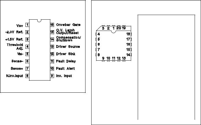
CONNECTION DIAGRAMS
DIL-16, SOIC-16 (TOP VIEW) |
J or N Package, DW Package |
PLCC-20, LCC-20 (TOP VIEW)
Q, L Packages
PACKAGE PIN FUNCTION
FUNCTION |
PIN |
N/C |
1 |
VIN + |
2 |
−2.0V REF |
3 |
+1.5V REF |
4 |
Threshold Adjust |
5 |
N/C |
6 |
VIN− |
7 |
Sense− |
8 |
Sense+ |
9 |
N.Inv. Input |
10 |
N/C |
11 |
Inv. Input |
12 |
Fault Alert |
13 |
Fault Delay |
14 |
Driver Sink |
15 |
N/C |
16 |
Driver Source |
17 |
Compensation/ Shutdown |
18 |
O.V. Latch Output/Reset |
19 |
Crowbar Gate |
20 |
2
UC1834
UC2834
UC3834 ELECTRICAL CHARACTERISTICS: Unless otherwise stated, these specifications apply for TA=−55°C to +125°C for the UC1834, −40°C to +85°C for the UC2834, and 0°C to +70°C for the
UC3834. VIN+ = 15V, VIN− = 0V, TA = TJ.
|
|
|
UC1834 |
|
|
UC3834 |
|
UNITS |
||||
PARAMETER |
TEST CONDITIONS |
|
UC2834 |
|
|
|
|
|
|
|
||
|
|
MIN |
|
TYP |
|
MAX |
MIN |
|
TYP |
|
MAX |
|
Turn-on Characteristics |
|
|
|
|
|
|
|
|
|
|
|
|
Standby Supply Current |
|
|
|
5.5 |
|
7 |
|
|
5.5 |
|
10 |
mA |
+1.5 Volt Reference |
|
|
|
|
|
|
|
|
|
|
|
|
Output Voltage |
TJ = 25°C |
1.485 |
|
1.5 |
|
1.515 |
1.47 |
|
1.5 |
|
1.53 |
V |
|
TJ(MIN) ≤ TJ ≤ TJ(MAX) |
1.47 |
|
|
|
1.53 |
1.455 |
|
|
|
1.545 |
|
Line Regulation |
VIN+ = 5 to 35V |
|
|
1 |
|
10 |
|
|
1 |
|
15 |
mV |
Load Regulation |
IOUT = 0 to 2mA |
|
|
1 |
|
10 |
|
|
1 |
|
15 |
mV |
-2.0 Volt Reference (Note 2) |
|
|
|
|
|
|
|
|
|
|
|
|
Output Voltage (Referenced |
TJ = 25°C |
−2.04 |
|
−2 |
|
−1.96 |
−2.06 |
|
−2 |
|
−1.94 |
V |
to VIN+) |
TJ(MIN) ≤ TJ ≤ TJ(MAX) |
−2.06 |
|
|
|
−1.94 |
−2.08 |
|
|
|
−1.92 |
|
Line Regulation |
VIN+ = 5 to 35V |
|
|
1.5 |
|
15 |
|
|
1.5 |
|
20 |
mV |
Output Impedance |
|
|
|
2.3 |
|
|
|
|
2.3 |
|
|
kΩ |
Error Amplifier Section |
|
|
|
|
|
|
|
|
|
|
|
|
Input Offset Voltage |
VCM = 1.5V |
|
|
1 |
|
6 |
|
|
1 |
|
10 |
mV |
Input Bias Current |
VCM = 1.5V |
|
|
−1 |
|
−4 |
|
|
−1 |
|
−8 |
μA |
Input Offset Current |
VCM = 1.5V |
|
|
0.1 |
|
1 |
|
|
0.1 |
|
2 |
μA |
Small Signal Open Loop Gain |
Output @ Pin 14, Pin 12 = VIN+ |
50 |
|
65 |
|
|
50 |
|
65 |
|
|
dB |
|
Pin 13, 20Ω to VIN− |
|
|
|
|
|
|
|
|
|
|
|
CMRR |
VCM = 0.5 to 33V, VIN+ = 35V |
60 |
|
80 |
|
|
60 |
|
80 |
|
|
dB |
PSRR |
VIN+ = 5 to 35V, VCM = 1.5V |
70 |
|
100 |
|
|
70 |
|
100 |
|
|
dB |
Driver Section |
|
|
|
|
|
|
|
|
|
|
|
|
Maximum Output Current |
|
200 |
|
350 |
|
|
200 |
|
350 |
|
|
mA |
Saturation Voltage |
IOUT = 100mA |
|
|
0.5 |
|
1.2 |
|
|
0.5 |
|
1.5 |
V |
Output Leakage Current |
Pin 12 = 35V, Pin 13 = VIN−, Pin 14 = VIN− |
|
|
0.1 |
|
50 |
|
|
0.1 |
|
50 |
μA |
Shutdown Input Voltage |
IOUT ≤ 100μA, Pin 13 = VIN−, Pin 12 = |
0.4 |
|
1 |
|
|
0.4 |
|
1 |
|
|
V |
at Pin 14 |
VIN+ |
|
|
|
|
|
|
|
|
|
|
|
Shutdown Input Current |
Pin 14 = VIN−, Pin 12 = VIN+ |
|
|
−100 |
|
−150 |
|
|
−100 |
|
−150 |
μA |
at Pin 14 |
IOUT ≤ 100μA, Pin 13 = VIN− |
|
|
|
|
|
|
|
|
|
|
|
Thermal Shutdown (Note 3) |
|
|
|
165 |
|
|
|
|
165 |
|
|
°C |
Fault Amplifier Section |
|
|
|
|
|
|
|
|
|
|
|
|
Underand Over-Voltage |
VCM = 1.5V, @ E/A Inputs |
120 |
150 |
|
180 |
110 |
150 |
|
190 |
mV |
||
Fault Threshold |
|
|
|
|
|
|
|
|
|
|
|
|
Common Mode Sensitivity |
VIN+ = 35V, VCM = 1.5 to 33V |
|
|
−0.4 |
−0.8 |
|
|
−0.4 |
−1.0 |
%/v |
||
Supply Sensitivity |
VCM = 1.5V, VIN+ = 5 to 35V |
|
|
−0.5 |
−1.0 |
|
|
−0.5 |
−1.2 |
%/V |
||
Fault Delay |
|
30 |
45 |
|
60 |
30 |
45 |
|
60 |
ms/μF |
||
Fault Alert Output Current |
|
2 |
5 |
|
|
2 |
5 |
|
|
mA |
||
Fault Alert Saturation Voltage |
IOUT = 1mA |
|
0.2 |
|
0.5 |
|
0.2 |
|
0.5 |
V |
||
O.V. Latch Output Current |
|
2 |
4 |
|
|
2 |
4 |
|
|
mA |
||
O.V. Latch Saturation Voltage IOUT = 1mA |
|
1.0 |
|
1.3 |
|
1.0 |
|
1.3 |
V |
|||
O.V. Latch Output Reset |
|
0.3 |
0.4 |
|
0.6 |
0.3 |
0.4 |
|
0.6 |
V |
||
Voltage |
|
|
|
|
|
|
|
|
|
|
|
|
Crowbar Gate Current |
|
−100 |
|
−175 |
|
−100 |
|
−175 |
|
mA |
||
Crowbar Gate Leakage |
VIN+ = 35V, Pin 16 = VIN− |
|
|
−0.5 |
−50 |
|
|
−0.5 |
−50 |
μA |
||
Current |
|
|
|
|
|
|
|
|
|
|
|
|
Note 2: When using both the 1.5V and −2.0V references the current out of pin 3 should be balanced by an equivalent current into Pin 2. The −2.0V output will change −2.3mV per μA of imbalance.
Note 3: Thermal shutdown turns off the driver. If Pin 15 (O.V. Latch Output) is tied to Pin 14 (Compensation/Shutdown) the O.V. Latch will be reset.
3
 Loading...