


Texas Instruments UC3872DWTR, UC3872DW, UC3872QTR, UC3872Q, UC3872N Datasheet
...
application
INFO
available
UC1872
UC2872
UC3872
Resonant Lamp Ballast Controller
FEATURES
•Controls Different Types of Lamps: Cold Cathode Fluorescent, Neon, and Gas Discharge
•Zero Voltage Switching (ZVS) of Push-Pull Drivers
•Accurate Control of Lamp Current
•Variable Lamp Intensity Control
•1 A Disable Current
•4.5V to 24V Operation
•Open Lamp Detection Circuitry
DESCRIPTION
The UC3872 is a resonant lamp ballast controller optimized for driving cold cathode fluorescent, neon, and other gas discharge lamps. The resonant power stage develops a sinusoidal lamp drive voltage, and minimizes switching loss and EMI generation. Lamp intensity adjustment is accomplished with a buck regulator, which is synchronized to the external power stage’s resonant frequency. Suitable for automotive and battery powered applications, the UC3872 draws only 1 A when disabled.
Soft start and open lamp detect circuitry have been incorporated to minimize component stresses. Open lamp detection is enabled at the completion of a soft start cycle. The chip is optimized for smooth duty cycle control to 100%.
Other features include a precision 1.2% reference, undervoltage lockout, and accurate minimum and maximum frequency control.
BLOCK DIAGRAM
VCC |
10 |
|
UVLO |
3.0V |
|
|
|
|
REF |
|
|
||||
|
|
|
|
|
|
||
REF |
9 |
|
|
|
|
|
|
ENBL |
(HIGH=ENABLE) |
|
|
|
|
PUSH PULL |
|
11 |
|
|
|
|
|
OUTPUTS |
|
|
|
|
|
|
|
|
|
|
|
|
|
|
0.1V |
+ |
N-CHANNEL |
COMP |
4 |
|
|
|
|
– |
|
INV |
6 |
|
– |
|
OPEN |
TOGGLE |
|
|
|
|
|||||
|
|
LAMP |
|
||||
|
|
EA |
|
|
|||
|
|
20 A |
+ |
|
DETECT |
T |
|
|
|
|
|
|
|||
|
|
|
1.5V |
|
|
PWM |
|
SS |
5 |
|
|
|
|
– |
|
|
|
|
|
– 1 |
|
||
|
|
|
|
200 |
A |
+ |
|
|
|
|
|
|
|
||
|
|
|
|
|
0.2V |
|
R |
CT |
7 |
|
|
|
+ |
|
S |
|
OSCILLATOR |
|
|
||||
|
|
|
|
|
|
||
|
ZERO DETECT |
SENSE |
|
|
|
|
|
|
OUT |
|
|
|
|
||
ZD |
8 |
|
|
|
|
BUCK DRIVE |
|
– |
SYNC |
|
|
|
|||
|
0.5V |
+ |
|
|
|
P-CHANNEL |
|
|
|
|
|
|
|
||
|
|
|
|
|
14 |
|
|
|
|
|
|
|
GND |
|
|
Note: Pin numbers shown are for DIP package.
3 |
VC |
2 |
AOUT |
50k |
|
1 |
BOUT |
50k |
|
50k |
|
12 |
COUT |
13 |
PGND |
UDG-99112 |
|
07/99
ABSOLUTE MAXIMUM RATINGS
Analog Inputs . . . . . . . . . . . . . . . . . . . . . . . . . . . . . −0.3 to +10V VCC, VC Voltage. . . . . . . . . . . . . . . . . . . . . . . . . . . . . . . . +24V ZD Input Current
High Impedance Source . . . . . . . . . . . . . . . . . . . . . . +10mA ZD Input Voltage
Low Impedance Source . . . . . . . . . . . . . . . . . . . . . . . . +24V Power Dissipation at TA = 25° C . . . . . . . . . . . . . . . . . . . . . . 1W Storage Temperature . . . . . . . . . . . . . . . . . . . −65° C to +150° C Lead Temperature. . . . . . . . . . . . . . . . . . . . . . . . . . . . . . 300° C
Note 1: Currents are positive into, negative out of the specified terminal.
Note 2: Consult Packaging Section of Databook for thermal limitations and considerations of package.
UC1872
UC2872
UC3872
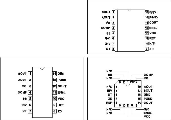
CONNECTION DIAGRAMS
SOIC-16, SSOP-16 (TOP VIEW)
DW, M Package
DIL-14 (TOP VIEW)
N Package
PLCC-20 (Top View)
Q Package
ELECTRICAL CHARACTERISTICS: Unless otherwise stated, these parameters apply for TJ = −55° C to +125°C for the UC1872, –40° C to +85° C for the UC2872, −0°C to +70°C for the UC3872; VCC= 5V, VC = 15V, VENBL = 5V, CT = 1nF, ZD = 1V.
PARAMETER |
TEST CONDITIONS |
MIN |
TYP |
MAX |
UNITS |
Reference Section |
|
|
|
|
|
Output Voltage |
TJ = 25° C |
2.963 |
3.000 |
3.037 |
V |
|
Over Temperature |
2.940 |
3.000 |
3.060 |
V |
Line Regulation |
VCC = 4.75V to 18V |
|
|
10 |
mV |
Load Regulation |
IO = 0 to −5mA |
|
|
10 |
mV |
Oscillator Section |
|
|
|
|
|
Free Running Frequency |
TJ = 25° C |
57 |
68 |
78 |
kHz |
Maximum Synchronization Frequency |
TJ = 25° C |
160 |
200 |
240 |
kHz |
Charge Current |
VCT = 1.5V |
180 |
200 |
220 |
µ A |
Voltage Stability |
|
|
|
2 |
% |
Temperature Stability |
|
|
4 |
8 |
% |
Zero Detect Threshold |
|
0.46 |
0.5 |
0.56 |
V |
Error Amp Section |
|
|
|
|
|
Input Voltage |
VO = 2V |
1.445 |
1.475 |
1.505 |
V |
Input Bias Current |
|
|
−0.4 |
−2 |
µ A |
Open Loop Gain |
VO = 0.5 to 3V |
65 |
90 |
|
dB |
Output High |
VINV = 1.3V |
3.1 |
3.5 |
3.9 |
V |
2
UC1872
UC2872
UC3872
ELECTRICAL CHARACTERISTICS: Unless otherwise stated, these parameters apply for TJ = −55° C to +125°C for the UC1872, –40° C to +85° C for the UC2872, −0°C to +70°C for the UC3872; VCC= 5V, VC = 15V, VENBL = 5V, CT = 1nF, ZD = 1V.
PARAMETER |
TEST CONDITIONS |
MIN |
TYP |
MAX |
UNITS |
Error Amp Section (cont.) |
|
|
|
|
|
Output Low |
VINV = 1.7V |
|
0.1 |
0.2 |
V |
Output Source Current |
VINV = 1.3V, VO = 2V |
–350 |
–500 |
|
A |
Output Sink Current |
VINV = 1.7V, VO = 2V |
10 |
20 |
|
mA |
Common Mode Range |
|
0 |
|
VIN-1V |
V |
Unity Gain Bandwidth |
TJ = 25° C (Note 4) |
|
1 |
|
MHz |
Open Lamp Detect Section |
|
|
|
|
|
Soft Start Threshold |
VINV = 0V |
2.9 |
3.4 |
3.8 |
V |
Open Lamp Detect Threshold |
VSS = 4.2V |
0.6 |
1.0 |
1.4 |
V |
Soft Start Current |
VSS = 2V |
10 |
20 |
40 |
µ A |
Output Section |
|
|
|
|
|
Output Low Level |
IOUT = 0, Outputs A and B |
|
0.05 |
0.2 |
V |
|
IOUT = 10mA |
|
0.1 |
0.4 |
V |
|
IOUT = 100mA |
|
1.5 |
2.2 |
V |
Output High Level |
IOUT = 0, Output C |
13.9 |
14.9 |
|
V |
|
IOUT = −10mA |
13.5 |
14.3 |
|
V |
|
IOUT = −100mA |
12.5 |
13.5 |
|
V |
Rise Time |
TJ = 25° C, Cl = 1nF (Note 4) |
|
30 |
80 |
ns |
Fall Time |
TJ = 25° C, Cl = 1nF (Note 4) |
|
30 |
80 |
ns |
Output Dynamics |
|
|
|
|
|
Out A and B Duty Cycle |
|
48 |
49.9 |
50 |
% |
Out C Max Duty Cycle |
VINV = 1V |
100 |
|
|
% |
Out C Min Duty Cycle |
VINV = 2V |
|
|
0 |
% |
Under Voltage Lockout Section |
|
|
|
|
|
Startup Threshold Voltage |
|
3.7 |
4.2 |
4.5 |
V |
Hysteresis |
|
120 |
200 |
280 |
mV |
Enable Section |
|
|
|
|
|
Input High Threshold |
|
2 |
|
|
V |
Input Low Threshold |
|
|
|
0.8 |
V |
Input Current |
VENBL = 5V |
|
150 |
400 |
µ A |
Supply Current Section |
|
|
|
|
|
VCC Supply Current |
VCC = 24V |
|
6 |
14 |
mA |
VC Supply Current |
VC = 24V |
|
5 |
12 |
mA |
ICC Disabled |
VCC = 24V, VENBL = 0V |
|
1 |
10 |
µ A |
Note 3: Unless otherwise specified, all voltages are with respect to ground. Currents are positive into, and negative out of the specified terminal.
Note 4: Guaranteed by design. Not 100% tested in production.
3
 Loading...