


Texas Instruments UC3874Q-1, UC3874N-2, UC3874N-1, UC3874DWTR-1, UC3874DW-2 Datasheet
...
UC1874-1,-2
UC2874-1,-2
UC3874-1,-2
High Efficiency, Synchronous, Step-down (Buck) Controllers
FEATURES
∙Operation to 36V Input Voltage
∙Fixed Frequency Average Current Mode Control
∙Standby Mode for Improved Efficiency at Light Load
∙Drives External N-Channel MOSFETs for Highest Efficiency
∙Sleep Mode Current < 50mA
∙Complementary 1 Amp Outputs with Regulated Gate Drive Voltage
∙LDO (Low Drop Out) Virtual 100% Duty Cycle Operation
∙Non-Overlapping Gate Drives
DESCRIPTION |
Not Recommended for New Designs. |
The UC3874 family of synchronous step-down (Buck) regulators provides high efficiency power conversion from an input voltage range of 4.5 to 36 volts. The UC3874 is tailored for battery powered applications such as laptop computers, consumer products, communications systems, and aerospace which demand high performance and long battery life. The synchronous regulator replaces the catch diode in the standard buck regulator with a low Rds(on) N-channel MOSFET switch allowing for significant efficiency improvements. The high side N-channel MOSFET switch is driven out of phase from the low side N-channel MOSFET switch by an on-chip bootstrap circuit which requires only a single external capacitor to develop the regulated gate drive. Fixed frequency, average current mode control provides the regulator with inherent slope compensation, tight regulation of the output voltage, and superior load and line transient response. Switching frequencies up to 300kHz are possible.
Light load efficiency is improved by a fully programmable standby mode, in which the quiescent current consumption of the controller is significantly reduced. The reduction is achieved by disabling the MOSFET driver outputs and the internal oscillator when the controller has sensed that the the output load current has dropped a user programmable amount from full load.
BLOCK DIAGRAM |
(continued) |
|
|
|
UDG-95005-1 |
2/98 |
|
During standby operation, the output capacitor supplies all of the load current requirements. Normal operation returns when the output voltage has drooped by 1%. Reverse current in the inductor is prevented by on-chip circuitry providing additional efficiency improvements. Virtual 100% duty cycle operation is easily attained by the controller even though a bootstrapped high side drive technique is employed.
A low power sleep mode can be invoked through the SS pin. Quiescent supply current in sleep mode is typically less than 50mA. Two UVLO options are available. The
UC1874-1,-2
UC2874-1,-2
UC3874-1,-2
UC3874-1 is designed for logic level MOSFETs and has UVLO turn-on and turn-off thresholds of 4.5V and 4.4V respectively. The UC3874-2 is designed for standard power MOSFETs and has UVLO turn-on and turn-off thresholds of 10V and 9V respectively. A precision 2.5V reference can supply 20mA to external circuitry. An error amplifier with soft start, high bandwidth current amplifier, and a synchronizable oscillator are additional features.
Available packages include 18-pin plastic and ceramic DIP (N, J), 18-pin SOIC (DW), and 20-pin plastic and ceramic leadless chip carriers (Q, L).
ABSOLUTE MAXIMUM RATINGS
Supply Voltage (VCC) . . . . . . . . . . . . . . . . . . . . . . . . . . . . . 36V Boost Voltage (BOOT). . . . . . . . . . . . . . . . . . . . . . . . . . . . . 50V OUTPUT Drivers (HDRIVE, LDRIVE) Currents
(continuous) . . . . . . . . . . . . . . . . . . . . . . . . . . . . . . . ±0.25A (peak) . . . . . . . . . . . . . . . . . . . . . . . . . . . . . . . . . . . . . . . ±1A VREF Current . . . . . . . . . . . . . . . . . . . . . . . . Internally Limited Inputs (VSNS, SS, COMP, CT) . . . . . . . . . . . . . . . . -0.3 to 10V Inputs (ISNS+, ISNS-) . . . . . . . . . . . . . . . . . . . . . . . -0.3 to 20V Outputs (CAOUT) . . . . . . . . . . . . . . . . . . . . . . . . . . . -0.3 to10V Soft start Sinking Current . . . . . . . . . . . . . . . . . . . . . . . . 1.5mA Storage Temperature . . . . . . . . . . . . . . . . . . . –65°C to +150°C Junction Temperature. . . . . . . . . . . . . . . . . . . –65°C to +150°C Lead Temperature (Soldering, 10 sec.) . . . . . . . . . . . . . +300°C
All currents are positive into, negative out of the specified terminal. All voltages are referenced to GND. Consult Packaging Section of Databook for thermal limitations and considerations of packages.
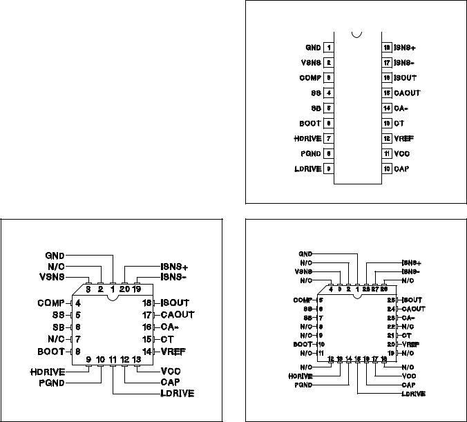
CONNECTION DIAGRAMS
DIL-18 (TOP VIEW)
J or N, DW Packages
PLCC-20 (TOP VIEW)
Q Package
LCC-28 (TOP VIEW)
L Package
2
UC1874-1,-2
UC2874-1,-2
UC3874-1,-2
ELECTRICAL CHARACTERISTICS: Unless otherwise stated these specifications apply for TA = –55°C to +125°C for UC1874; TA = –25°C to +85°C for UC2874; 0°C to +70°C for UC3874; VCC = 12V, Ct = 680pF, C CAP = 1μF; CBOOT = 0.1μF; TA = TJ.
PARAMETER |
TEST CONDITIONS |
MIN |
TYP |
MAX |
UNITS |
Overall Section |
|
|
|
|
|
Supply Current, Sleep |
SOFTSTART = 0V; TA=25°C |
|
30 |
75 |
μA |
Supply Current, Operating |
|
|
8.5 |
12 |
mA |
Supply Current, Standby |
UC2874-1, -2, UC3874-1, -2 |
|
2.5 |
3.5 |
mA |
Supply Current, Standby |
UC1874-1, -2 |
|
|
5.5 |
mA |
VCC Turn-on Threshold |
UCX874-2 |
|
10 |
10.5 |
V |
|
UCX874-1 |
|
4.5 |
4.8 |
V |
VCC Turn-off Threshold |
UCX874-2 |
8.5 |
9 |
|
V |
|
UCX874-1 |
4.1 |
4.4 |
|
V |
Voltage Amplifier Section |
|
|
|
|
|
Input Voltage |
TA = 25°C |
1.97 |
2 |
2.03 |
V |
VSNS Bias Current |
|
–500 |
25 |
500 |
nA |
Transconductance |
ICOMp = +10μA to –10μA, UC3874 -1, -2; |
400 |
675 |
1000 |
μMho |
|
UC2874-1, -2 |
|
|
|
|
Transconductance |
ICOMp = +5μA to –5μA, UC1874-1,-2 |
250 |
675 |
1250 |
μMho |
VOUT High |
|
2.9 |
3.1 |
3.25 |
V |
VOUT Low |
SB = VREF |
|
|
1.85 |
V |
Output Source Current |
VOUT = 1V; UC3874-1,-2; UC2874-1,-2 |
10 |
35 |
|
μA |
|
VOUT = 1V; UC1874 -1,-2 |
5 |
35 |
|
μA |
Current Amplifier Section |
|
|
|
|
|
Input Offset Voltage |
VCOMP = 2.5V |
–6 |
0 |
6 |
mV |
Input Bias Current (SENSE) |
VCM = 2.5V |
–500 |
|
500 |
nA |
Open Loop Gain |
VCM = 2.5V, VOUT = 1V to 3.5V |
80 |
110 |
|
dB |
VOUT High |
RCAOUT = 100k to GND, TA = 25°C |
3.6 |
3.7 |
|
V |
VOUT Low |
RCAOUT = 100k to VREF, TA = 25°C |
|
0.7 |
0.86 |
V |
Output Source Current |
VOUT = 0V, TA = 25°C |
80 |
100 |
120 |
μA |
Common Mode REJ Ratio |
VCM = 2V to 3V |
70 |
90 |
|
dB |
Gain Bandwidth Product |
FIN = 100kHz, 10mV p-p |
2 |
3.5 |
|
MHz |
Reference Section |
|
|
|
|
|
Output Voltage |
IREF = 0mA, TA = 25°C |
2.462 |
2.5 |
2.538 |
V |
|
IREF = 0mA |
2.437 |
2.5 |
2.563 |
V |
Load Regulation |
IREF = 0mA to 5mA |
|
2 |
± 15 |
mV |
Line Regulation |
VCC = 12V to 24V |
|
2 |
± 15 |
mV |
Short Circuit Current |
VREF = 0V |
10 |
20 |
25 |
mA |
Oscillator Section |
|
|
|
|
|
Initial Accuracy |
TA = 25°C |
85 |
100 |
115 |
kHz |
Voltage Stability |
VCC = 12V to 18V |
|
1 |
1.5 |
% |
Total Variation |
Line, Temperature |
80 |
|
120 |
kHz |
Ramp Amplitude (p-p) |
TA = 25°C |
2.48 |
2.7 |
2.85 |
V |
Ramp Valley Voltage |
TA = 25°C |
0.86 |
0.95 |
|
V |
Sleep/Soft Start/Bootstrap Section |
|
|
|
|
|
Sleep Threshold |
Measured on SS, TA = 25°C |
0.25 |
0.6 |
0.8 |
V |
SS Charge Current |
VSS = 2.5V |
4 |
6 |
10 |
μA |
3
 Loading...