


Texas Instruments UCC384DPTR-ADJ, UCC384DPTR-5, UCC384DP-ADJ, UCC384DP-5, UCC384DP-12 Datasheet
...
UCC284-5/-12/-ADJ
UCC384-5/-12/-ADJ
Low Dropout 0.5A Negative Linear Regulator
FEATURES |
BLOCK DIAGRAM |
•Precision Negative Series Pass Voltage Regulation
•0.2V Drop Out at 0.5A
•Wide Input voltage Range –3.2V to –15V
•Low Quiescent Current Irrespective of Load
•Simple Logic Shutdown Interfacing
•–5V, –12V and Adjustable Output
•2.5% Duty Cycle Short Circuit Protection
•Remote Load Sensing for Accurate Load Regulation
•8-Pin DP Package
|
|
|
|
|
|
|
|
|
|
|
(+) |
|
1 A |
|
|
|
|
|
|
|
|
4 |
GND |
|
|
|
|
|
|
|
R1 |
R2 |
|
|
|
|
DISCHARGE |
|
|
|
|
|
|
|
|||
|
|
|
|
|
|
|
|
|
|
||
|
|
+ |
|
|
|
|
UCC384-ADJ |
0 |
OPEN |
|
|
|
|
SHUTDOWN |
–2.2V |
UCC384-5 |
375K |
125K |
|
|
|||
|
|
|
|
|
|||||||
|
–0.6V |
– |
|
|
|
|
1.25V |
|
|
R2 |
|
|
|
50k |
|
|
|
|
UCC384-12 |
375K |
43.6K |
|
|
|
|
|
|
|
|
|
|
||||
|
|
+ |
|
|
|
|
|
|
|
|
|
|
–1.6V |
– |
S |
Q |
TON |
|
|
|
|
|
|
|
|
|
|
|
|
|
|
|
|||
SD/CT |
8 |
|
|
|
|
|
|
|
|
||
|
|
|
|
|
|
|
|
|
|
||
|
|
|
R |
Q |
TOFF |
|
|
VPUMP |
|
|
|
|
–2.6V |
+ |
|
|
|
|
|
|
|||
|
|
|
|
|
|
|
|
|
|
||
|
|
– |
|
|
|
|
+ |
|
|
R1 |
|
|
|
|
|
|
|
|
|
|
|
||
|
|
|
|
|
|
|
GM |
|
|
|
|
|
40 A |
|
|
|
|
|
– |
|
|
|
|
|
|
|
|
|
|
|
|
|
|
|
|
|
CHARGE |
|
|
|
|
|
|
|
|
1 |
VOUTS |
|
|
|
|
|
|
|
|
|
|
||
|
OVERCURRENT |
|
|
|
|
|
|
|
|
||
|
|
700mA |
– |
|
|
|
|
|
|
|
|
|
|
|
+ |
|
|
|
|
|
|
|
|
VIN |
2 |
THERMAL |
|
|
|
|
|
|
|
|
|
|
|
|
|
|
|
|
|
|
|
||
VIN |
3 |
SHUTDOWN |
|
|
|
|
|
|
|
|
|
|
|
|
|
|
|
|
|
|
|
||
VIN |
6 |
|
UVLO |
|
|
|
|
|
|
|
|
|
|
|
|
|
|
|
|
|
|
|
|
VIN |
7 |
|
|
|
|
|
|
|
|
5 |
VOUT |
(–) |
|
|
|
|
|
|
|
|
|
|
(–) |
|
|
|
|
|
|
|
|
|
|
UDG-99030 |
|
DESCRIPTION
The UCC384 family of negative linear series pass regulators is tailored for low drop out applications where low quiescent power is important. Fabricated with a BCDMOS technology ideally suited for low input to output differential applications, the UCC384 will pass 0.5A while requiring only 0.2V of input voltage headroom. Drop out voltage decreases linearly with output current, so that drop out at 50mA is less than 20mV.
Quiescent current consumption for the device under normal (non-drop out) conditions is typically 200 A. An integrated charge pump is internally enabled only when the device is operating near drop out with low VIN. This guarantees that the device will meet the drop out specifications even for maximum load current and a VIN of –3.2V with only a modest increase in quiescent current. Quiescent current is always less than 350 A, with the charge pump enabled. Quiescent current of the UCC384 does not increase with load current.
SLUS234A - JANUARY 2000
Short circuit current is internally limited. The device responds to a sustained over current condition by turning off after a TON delay. The device then stays off for a pe-
riod, TOFF, that is 40 times the TON delay. The device then begins pulsing on and off at the TON/TOFF duty cycle of 2.5%. This drastically reduces the power dissipation
during short circuit such that heat sinking, if at all required, must only accommodate normal operation. An external capacitor sets the on time. The off time is always 40 times TON.
The UCC384 can be shutdown to 45 A (maximum) by pulling the SD/CT pin more positive than –0.6V. To allow for simpler interfacing, the SD/CT pin may be pulled up to +6V above the ground pin without turning on clamping diodes.
Internal power dissipation is further controlled with thermal overload protection circuitry. Thermal shutdown occurs if the junction temperature exceeds 140°C. The chip will remain off until the temperature has dropped 20°C.
ABSOLUTE MAXIMUM RATINGS
Supply Voltage, VIN . . . . . . . . . . . . . . . . . . . . . . . . . . . . . –16V Shutdown Voltage, SD/CT . . . . . . . . . . . . . . . . . . . . +6V to –5V Storage Temperature . . . . . . . . . . . . . . . . . . . −65°C to +150°C Junction Temperature. . . . . . . . . . . . . . . . . . . –55°C to +150°C Lead Temperature (Soldering, 10 sec.) . . . . . . . . . . . . . +300°C
All voltages are with respect to ground. Currents are positive into, negative out of the specified terminal. All voltages are with respect to ground. Consult Packaging Section of Databook for thermal limitations and considerations of packages.
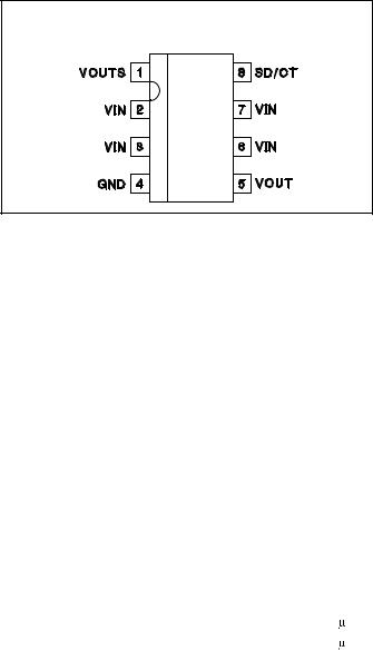
UCC284-5/-12/-ADJ
UCC384-5/-12/-ADJ
CONNECTION DIAGRAM
SOIC-8 (Top View)
DP Package
ELECTRICAL CHARACTERISTICS: Unless otherwise specified, TA = 0°C to 70°C for the UCC384 and –40°C to 85°C for the UCC284, VIN = VOUT – 1.5V, IOUT = 0mA, COUT = 4.7µF, and CT = 0.015µF. For UCC384-ADJ, VOUT is set to –3.3V. TJ = TA.
PARAMETER |
|
TEST CONDITIONS |
MIN |
TYP |
MAX |
UNITS |
UCC384-5 Fixed –5V 0.5A Regulation Section |
|
|
|
|
|
|
Output Voltage |
|
TA = 25°C |
–5.075 |
–5 |
–4.925 |
V |
|
|
Over all conditions |
–5.100 |
|
–4.850 |
V |
Line Regulation |
|
VIN = –5.3V to –15V |
|
1.5 |
10 |
mV |
Load Regulation |
|
IOUT = 0mA to 0.5A |
|
0.1 |
0.25 |
% |
Output Noise Voltage |
|
TA = 25°C, BW = 10Hz to 10kHz |
|
200 |
|
µVRMS |
Drop Out Voltage, VOUT – VIN |
|
IOUT 0.5A, VOUT = –4.8V |
|
0.20 |
0.50 |
V |
|
|
IOUT 50mA, VOUT = –4.8V |
|
20 |
50 |
mV |
UCC384-5 Fixed –5V 0.5A Power Supply Section |
|
|
|
|
||
Input Voltage Range |
|
|
–15 |
|
–5.2 |
V |
Quiescent Current Charge Pump On |
|
VIN = –4.85V (Note 1) |
|
280 |
350 |
µA |
Quiescent Current |
|
VIN = –15V |
|
200 |
250 |
µA |
Quiescent Current in Shutdown |
|
VIN = –15V, SD/CT = 0V, No Load |
|
24 |
45 |
µA |
Shutdown Threshold |
|
At Shutdown Pin |
–1.0 |
–0.6 |
–0.4 |
V |
Shutdown Input Current |
|
SD/CT = 0V |
5 |
17 |
25 |
µA |
Output Leakage in Shutdown |
|
VIN = –15V, VOUT = 0, 25°C |
|
1 |
10 |
A |
|
|
Over Temperature |
|
|
50 |
A |
Over Temperature Shutdown |
|
|
|
140 |
|
°C |
Over Temperature Hysteresis |
|
|
|
20 |
|
°C |
UCC384-5 Fixed –5V 0.5A Current Limit Section |
|
|
|
|
||
Peak Current Limit |
|
VOUT = 0V |
0.7 |
1.1 |
1.5 |
A |
Over Current Threshold |
|
|
0.55 |
0.7 |
0.9 |
A |
Current Limit Duty Cycle |
|
VOUT = 0V |
|
2.5 |
4 |
% |
Overcurrent Time Out, TON |
|
VOUT = 0V |
300 |
450 |
650 |
µs |
UCC384-12 Fixed 12V 0.5A Regulation Section |
|
|
|
|
||
Output Voltage |
|
TA = 25°C |
–12.18 |
–12 |
–11.82 |
V |
|
|
Over all conditions |
–12.24 |
|
–11.64 |
V |
Line Regulation |
|
VIN = –12.5V to –15V |
|
5 |
15 |
mV |
Load Regulation |
|
IOUT = 0mA to 0.5A |
|
0.1 |
0.3 |
% |
Output Noise Voltage |
|
TA = 25°C, BW = 10Hz to 10kHz |
|
200 |
|
µVRMS |
Drop Out Voltage, VOUT - VIN |
|
IOUT 0.5A, VOUT = –11.6V |
|
0.15 |
0.5 |
V |
|
|
IOUT 50mA, VOUT = –11.6V |
|
15 |
50 |
mV |
2
UCC284-5/-12/-ADJ
UCC384-5/-12/-ADJ
ELECTRICAL CHARACTERISTICS: Unless otherwise specified, TA = 0°C to 70°C for the UCC384 and –40°C to 85°C for the UCC284, VIN = VOUT – 1.5V, IOUT = 0mA, COUT = 4.7 F, and CT = 0.015 F. For UCC384-ADJ, VOUT is set to –3.3V. TJ = TA.
PARAMETER |
TEST CONDITIONS |
MIN |
TYP |
MAX |
UNITS |
UCC384-12 Fixed –12V 0.5A Power Supply Section |
|
|
|
|
|
Input Voltage Range |
|
–15 |
|
–12.2 |
V |
Quiescent Current |
VIN = –15V |
|
220 |
350 |
A |
Quiescent Current in Shutdown |
VIN = –15V, SD/CT = 0V, No Load |
|
24 |
45 |
A |
Shutdown Threshold |
At Shutdown Pin |
–1.0 |
–0.6 |
–0.4 |
V |
Shutdown Input Current |
SD/CT = 0V |
5 |
17 |
25 |
A |
Output Leakage in Shutdown |
VIN = –15V, VOUT = 0, 25°C |
|
1 |
10 |
A |
|
Over Temperature |
|
|
50 |
A |
Over Temperature Shutdown |
|
|
140 |
|
°C |
Over Temperature Hysteresis |
|
|
20 |
|
°C |
UCC384-12 Fixed -12V 0.5A Current Limit Section |
|
|
|
|
|
Peak Current Limit |
VOUT = 0V |
0.7 |
1.2 |
1.5 |
A |
Over Current Threshold |
|
0.55 |
0.7 |
0.9 |
A |
Current Limit Duty Cycle |
VOUT = 0V |
|
2.5 |
4 |
% |
Over Current Time Out, TON |
VOUT = 0V |
300 |
450 |
650 |
s |
UCC384-ADJ Adjustable 0.5A Regulation Section |
|
|
|
|
|
Reference Voltage |
TA = 25°C |
–1.27 |
–1.25 |
–1.23 |
V |
|
Over Temperature |
–1.275 |
|
–1.215 |
V |
Line Regulation |
VIN = –3.5V to –15V, VOUT = VOUTS |
|
0.5 |
3 |
mV |
Load Regulation |
IOUT = 0mA to 0.5A |
|
0.1 |
0.18 |
% |
Output Noise Voltage |
TA = 25°C, BW = 10Hz to 10kHz |
|
200 |
|
VRMS |
Drop Out Voltage, VOUT - VIN |
IOUT 0.5A, VOUT = –3.15V |
|
0.25 |
0.5 |
V |
|
IOUT 50mA, VOUT = 3.15V |
|
25 |
50 |
mV |
Sense Pin Input Current |
|
|
100 |
250 |
nA |
UCC384-ADJ Adjustable 0.5A Power Supply Section |
|
|
|
|
|
Input Voltage Range |
|
–15 |
|
–3.5 |
V |
Undervoltage Lockout |
|
–3.2 |
|
–2.7 |
V |
Quiescent Current Charge Pump On |
VIN = –3.15V (Note 1) |
|
200 |
350 |
A |
Quiescent Current |
VIN = –15V |
|
200 |
250 |
A |
Quiescent Current in Shutdown |
VIN = –15V, SD/CT = 0V, No Load |
|
24 |
45 |
A |
Shutdown Threshold |
At Shutdown Pin |
–1.0 |
–0.6 |
–0.4 |
V |
Shutdown Input Current |
SD/CT = 0V |
5 |
17 |
25 |
A |
Output Leakage in Shutdown |
VIN = –15V, VOUT = 0, 25°C |
|
1 |
10 |
A |
|
Over Temperature |
|
|
50 |
A |
Over Temperature Shutdown |
|
|
140 |
|
°C |
Over Temperature Hysteresis |
|
|
20 |
|
°C |
UCC384-ADJ Adjustable 0.5A Current Limit Section |
|
|
|
|
|
Peak Current Limit |
VOUT = 0V |
0.7 |
1.1 |
1.5 |
A |
Over Current Threshold |
|
0.55 |
0.7 |
0.9 |
A |
Current Limit Duty Cycle |
VOUT = 0V |
|
2.5 |
4 |
% |
Over Current Time Out, TON |
VOUT = 0V |
300 |
450 |
650 |
s |
Note 1: Internal Charge Pump is enabled only for drop-out condition with low VIN. Only in this condition is the Charge Pump required to provide additional output FET gate drive to maintain drop-out specifications. For conditions where the Charge Pump is not required, it is disabled, which lowers overall device power consumption.
3
 Loading...