Texas Instruments UC5605PWP, UC5605N, UC5605DPTR, UC5605DP, UC5605Z Datasheet
...
UC5605
9-Line Low Capacitance SCSI Active Terminator
FEATURES
∙Reverse Disconnect
∙Complies with SCSI, SCSI-2 and SPI-2 Standards
∙5pF Channel Capacitance during Disconnect
∙Hot Plugging Capability
∙−400mA Sourcing Current for Termination
∙+100mA Sinking Current for Active Negation
∙1V Dropout Voltage Regulator
∙100μA Supply Current in Disconnect Mode
∙Trimmed Termination Current to 5%
∙Trimmed Impedance to 5%
∙Low Thermal Resistance Surface Mount Packages
DESCRIPTION
The UC5605 provides 9 lines of active termination for a SCSI (Small Computer Systems Interface) parallel bus. The SCSI standard recommends active termination at both ends of the cable segment.
The only functional differences between the UC5603 and UC5605 is the absence of the negative clamps on the output lines and the disconnect input must be at a logic-low for the terminating resistors to be disconnected. Parametrically, the UC5605 has a 5% tolerance on impedance and current compared to a 3% tolerance on the UC5603. Custom power packages are utilized to allow normal operation at full power (2 Watts).
The UC5605 provides a disconnect feature which, when driven low, disconnects all terminating resistors, disables the regulator and greatly reduces standby power consumption. The output channels remain high impedance even without Termpwr applied. A low channel capacitance of 5pF allows interim points of the bus to have little to no effect on the signal integrity.
Internal circuit trimming is utilized, first to trim the impedance to a 5% tolerance, and then most importantly, to trim the output current to a 5% tolerance, as close to the maximum SCSI specification as possible. This maximizes the noise margin in fast SCSI operation. Other features include thermal shutdown and current limit.
This device is offered in low thermal resistance versions of the industry standard 16 pin narrow body SOIC, 16 pin ZIP (zig-zag in line package) and 24 pin TSSOP.
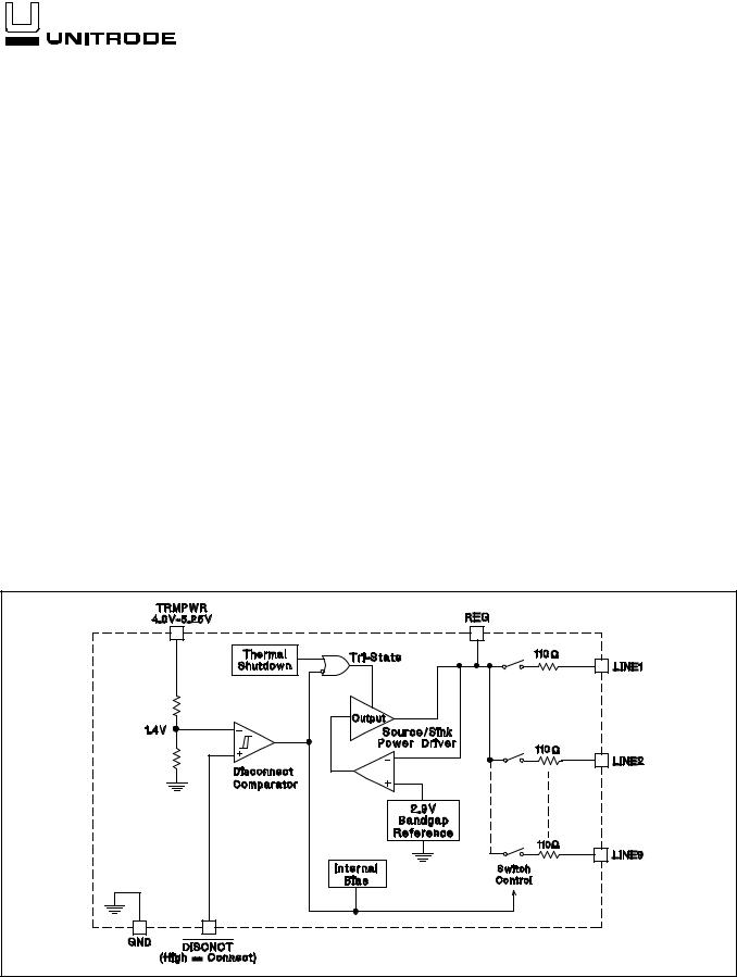
BLOCK DIAGRAM
UDG-94122
Circuit Design Patented
3/97

ABSOLUTE MAXIMUM RATINGS
Termpwr Voltage . . . . . . . . . . . . . . . . . . . . . . . . . . . . . . . . . +7V Signal Line Voltage. . . . . . . . . . . . . . . . . . . . . . . . . . . 0V to +7V Regulator Output Current . . . . . . . . . . . . . . . . . . . . . . . . . . 0.6A Storage Temperature . . . . . . . . . . . . . . . . . . . −65°C to +150°C Operating Temperature . . . . . . . . . . . . . . . . . −55°C to +150°C Lead Temperature (Soldering, 10 Sec.) . . . . . . . . . . . . . +300°C
Unless otherwise specified all voltages are with respect to Ground. Currents are positive into, negative out of the specified terminal.
Consult Packaging Section of Unitrode Integrated Circuits databook for thermal limitations and considerations of packages.
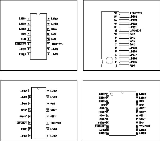
CONNECTION DIAGRAMS
DIL-16 (Top View)
N or J Package
SOIC-16 (Top View)
DP Package
UC5605
RECOMMENDED OPERATING CONDITIONS
Termpwr Voltage . . . . . . . . . . . . . . . . . . . . . . . . . 3.8V to 5.25V Signal Line Voltage. . . . . . . . . . . . . . . . . . . . . . . . . . . 0V to +5V Disconnect Input Voltage . . . . . . . . . . . . . . . . . . 0V to Termpwr
ZIP-16 (Top View)
Z Package
TSSOP-24 (Top View)
PWP Package
* DP package pin 5 serves as signal ground; pins 4, 12, 13 serve as heatsink/ground.
Note: Drawings are not to scale.
* PWP package pin 9 serves as signal ground; pins 5, 6, 7, 8, 17, 18, 19, and 20 serve as heatsink/ground.
2
 Loading...