


TEXAS INSTRUMENTS UCC2975, UCC2976, UCC2977, UCC3975, UCC3976 Technical data
...UCC2976PW
UCC2975, UCC2976, UCC2977
UCC3975, UCC3976, UCC3977
SLUS499A – NOVEMBER 2001 – REVISED JANUARY 2002
MULTI TOPOLOGY PIEZOELECTRIC
TRANSFORMER CONTROLLER
FEATURES
D3-V to 13.5-V Operation
DSupports Flyback (UCC3975), Half-Bridge (UCC3976), and Push-Pull (UCC3977) Topologies
DProgrammable Voltage Controlled Oscillator
DOpen Lamp Protection
DLow Shutdown Current (15- A Typical)
DDual MOSFET Drivers
D8-Pin TSSOP package
APPLICATIONS
DNotebook Computers
DPortable Electronics Displays
DPortable Instruments
DESCRIPTION
Liquid crystal display (LCD) enclosures and cold cathode fluorescent lamps (CCFLs) used in notebook computer and portable electronics displays are becoming increasingly narrow, generating the need for a low profile CCFL power supply. Recent advances in singleand multi-layered piezoelectric ceramic transformers (PZT) have enabled the development of a new generation of efficient, size-reduced backlight converters. The UCC3975/6/7 family of 8-pin PZT controllers integrate the necessary circuitry for operating a PZT-based backlight supply using a flyback, half-bridge, or push-pull topology. The choice of power topology depends on application requirements such as input voltage, lamp voltage, and PZT gain.
|
|
|
|
|
DOPEN |
|
SHUTDOWN |
|
|
|
|
VDD |
|
|
|
|
|
|
|
|
|
1 |
OPEN/SD |
VDD |
8 |
COPEN |
ROPEN |
|
|
|
||||
|
2 |
OSC |
OUTP |
7 |
LRES |
RHV |
|
COSC |
|
|
|
|
|
|
UCC3976 |
|
|
|
||
ROSC |
RANGE |
|
|
|
||
|
3 |
COMP |
OUTN |
6 |
PIEZO |
|
|
|
|
|
|
||
RCNT |
CFB |
|
|
|
XFMR |
|
|
|
|
|
|
||
|
4 |
FB |
GND |
5 |
|
|
RFB DFB
CCFL
RCS
UDG–01092
Figure 1. UCC3976-Based CCFL Power Supply Using a Resonant Half-Bridge Topology
|
|
|
PRODUCTION DATA information is current as of publication date. |
Copyright 2002, Texas Instruments Incorporated |
|
Products conform to specifications per the terms of Texas Instruments |
|
|
standard warranty. Production processing does not necessarily include |
|
|
testing of all parameters. |
|
|
www.ti.com |
1 |

UCC2975, UCC2976, UCC2977
UCC3975, UCC3976, UCC3977
SLUS499A – NOVEMBER 2001 – REVISED JANUARY 2002
description (continued)
A half-bridge PZT converter, using the UCC3976 is shown in Figure 1. External P- and N-channel MOSFETs are driven out of phase at a fixed 50% duty cycle with anti-cross conduction circuitry provided by the controller. The half-bridge topology uses only a single magnetic component (LRES) reducing board area. As explained in the applications section of this datasheet, regulation of lamp current is achieved by controlling the operating frequency of the system.
The UCC3977 is designed to control a resonant push-pull topology as shown in Figure 2. This controller alternately drives external N-channel MOSFETs at 50% duty cycle. The push-pull topology requires two external inductors (L1 and L2), but has the advantage of providing increased voltage across the piezoelectric transformer primary. In this case a small overlap is provided to the gate drives, assuring an uninterrupted path for inductor current.
DOPEN
SHUTDOWN |
|
|
|
|
|
|
|
|
|
|
|
COPEN |
ROPEN |
|
|
|
|
|
|
VDD |
|
|
1 |
OPEN/SD |
VDD |
8 |
|
|
|
|
|
|
L1 |
L2 |
|
|
|
UCC3977 |
|
PIEZO XFMR |
|
|
|
|
|
|
|
|
|
|
2 |
OSC |
|
N1 |
RHV |
|
|
|
N2 |
|||
|
|
|
|
|
||
ROSC |
COSC |
|
|
OUT1 |
7 |
|
RANGE |
|
|
||||
|
|
|
|
|
|
|
|
|
3 |
COMP |
OUT2 6 |
|
|
RCNT |
|
CFB |
|
|
|
|
VCNT |
|
4 |
FB |
GND |
5 |
|
|
|
|
|
|
|
|
|
|
RFB D |
|
|
|
|
|
|
FB |
|
|
|
|
|
|
RCS |
|
|
CCFL |
|
|
|
|
|
|
|
|
UDG–01097
Figure 2. UCC3977 Based CCFL Power Supply Using a Resonant Push-Pull Topology
For piezoelectric transformer applications requiring additional gain, a resonant flyback topology can be implemented using the UCC3975. As shown in Figure 3, a magnetic transformer (T1) provides a stepped up voltage to the piezoelectric transformer primary. When compared to a traditional high-voltage transformer used in a CCFL application, T1 is small and low profile because of its reduced turns ratio and voltage rating. In the resonant flyback application, a single switch is driven at 50% duty cycle producing a half wave rectified sinusoid at the piezoelectric transformer primary.
2 |
www.ti.com |

UCC2975, UCC2976, UCC2977
UCC3975, UCC3976, UCC3977
SLUS499A – NOVEMBER 2001 – REVISED JANUARY 2002
description (continued)
SHUTDOWN |
|
|
|
|
|
|
|
|
|
|
|
COPEN |
ROPEN |
|
|
|
|
|
VDD |
|
|
|
1 |
OPEN/SD |
VDD |
8 |
|
|
|
|
UCC3975 |
PIEZO |
|
|
|
|
2 |
OSC |
|
XFMR |
|
|
|
|
|
RHV |
||
ROSC |
COSC |
|
|
OUTP |
7 |
|
RANGE |
|
|
||||
|
|
|
|
|
|
|
|
|
|
|
|
N |
|
|
|
3 |
COMP |
OUTN |
6 |
|
|
RCNT |
CFB |
|
|
|
|
VCNT |
|
4 |
FB |
GND |
5 |
|
|
|
|
|
|
|
|
|
|
RFB D |
|
|
|
|
|
|
FB |
|
|
|
|
|
|
RCS |
|
|
CCFL |
|
|
|
|
|
|
|
|
|
|
|
|
|
|
UDG–01098 |
Figure 3. UCC3975-Based CCFL Power Supply Using a Resonant Flyback Topology |
||||||
absolute maximum ratings over operating free-air temperature (unless otherwise noted)† |
||||||
Supply voltage |
VDD . . |
. . . . . . . . |
. . . . . . . . |
. . . . . . |
. . . . . . . . . . . . . . . . . . . . . . . |
. . . . . . . . . . . . . . . . . . . 15 V |
Input voltage |
OPEN/SD, OSC, COMP, FB, VDD, OUTP . . . . . . . . . . . . . . |
GND–0.5 V to VDD+0.5 V |
||||
Storage temperature range, Tstg . . . . . . |
. . . . . . . . |
. . . . . . |
. . . . . . . . . . . . . . . . . . . . . . . |
. . . . . . . . . –65° C to 150° C |
||
Junction temperature range, TJ . . . . . . . |
. . . . . . . . |
. . . . . . |
. . . . . . . . . . . . . . . . . . . . . . . |
. . . . . . . . –40° C to 125° C |
||
Lead temperature 1,6 mm (1/16 inch) from case for 10 seconds . . . . . . . . . . . . . . . . |
. . . . . . . . . . . . . . . . 300° C |
|||||
† Stresses beyond those listed under “absolute maximum ratings” may cause permanent damage to the device. These are stress ratings only, and functional operation of the device at these or any other conditions beyond those indicated under “recommended operating conditions” is not implied. Exposure to absolute-maximum-rated conditions for extended periods may affect device reliability.
§ All voltages are respect to GND.
AVAILABLE OPTIONS
|
PACKAGED DEVICES† TSSOP (PW) |
||
TA |
|
TOPOLOGY |
|
|
FLYBACK |
HALF-BRIDGE |
PUSH-PULL |
|
|
|
|
–40° C to 85° C |
UCC2975PW |
UCC2976PW |
UCC2977PW |
|
|
|
|
0° C to 70° C |
UCC3975PW |
UCC3976PW |
UCC3977PW |
†The PW package is available taped and reeled. Add TR suffix to device type (e.g. UCC2975TRPW) to order quantities of 2500 devices per reel.
www.ti.com |
3 |

UCC2975, UCC2976, UCC2977
UCC3975, UCC3976, UCC3977
SLUS499A – NOVEMBER 2001 – REVISED JANUARY 2002
electrical characteristics VDD = 3 V to 13.5 V, TA = 0° C to 70° C for UCC3975/UCC3976/UCC3977, TA = –40° C to 85° C for the UCC2975/UCC2976/UCC2977, TA = TJ (unless otherwise noted)
input supply
PARAMETER |
|
TEST CONDITIONS |
MIN |
TYP |
MAX |
UNITS |
|
|
|
|
|
|
|
VDD supply current |
Normal, |
VDD = 12 V |
|
1 |
2.5 |
mA |
Shutdown |
|
|
20 |
100 |
µ A |
|
|
|
|
||||
|
|
|
|
|
|
|
VDD UVLO (turn-on) threshold voltage |
|
|
2.70 |
2.85 |
3.00 |
V |
|
|
|
|
|
|
|
UVLO hysteresis |
|
|
100 |
200 |
300 |
mV |
|
|
|
|
|
|
|
output
PARAMETER |
TEST CONDITIONS |
MIN |
TYP |
MAX |
UNITS |
|
|
|
|
|
|
|
|
P–channel driver output voltage, VOUTP |
IPIN = 100 mA, |
Driving logic low |
|
0.5 |
0.9 |
|
P-channel driver output voltage, (VDD – VOUTP) |
IPIN = –100 mA, |
Driving logic high |
|
0.5 |
0.9 |
|
Low-level N–channel driver output voltage, VOUTN |
IPIN = 100 mA, |
Driving logic low |
|
0.5 |
0.9 |
V |
High-level N–channel driver output voltage, |
IPIN = –100 mA, |
Driving logic high |
|
0.5 |
0.9 |
|
(VDD – VOUTN) |
|
|
||||
|
|
|
|
|
|
|
Rise time |
VDD = 5 V, |
CL = 1 nF, |
|
200 |
|
|
|
|
|
|
|
||
Fall time |
See Note 1 |
|
|
200 |
|
ns |
Dead (overlap) time |
See Note 1 |
|
|
250 |
|
|
|
|
|
|
|
|
|
oscillator
PARAMETER |
TEST CONDITIONS |
MIN |
TYP |
MAX |
UNITS |
|
|
|
|
|
|
Upper threshold voltage |
|
1.6 |
1.7 |
1.8 |
V |
|
|
|
|
|
|
Lower threshold voltage |
|
0.65 |
0.70 |
0.80 |
|
|
|
||||
|
|
|
|
|
|
Frequency |
ROSC = 24 kΩ , COSC = 470 pF |
95 |
100 |
105 |
kHz |
error amplifier
PARAMETER |
TEST CONDITIONS |
MIN |
TYP |
MAX |
UNITS |
||
|
|
|
|
|
|
|
|
Input voltage |
|
|
|
1.465 |
1.500 |
1.535 |
V |
|
|
|
|
|
|
|
|
Line regulation voltage |
3 V ≤ VDD ≤ 13.5 V |
|
|
–2 |
2 |
6 |
mV |
Input bias current |
|
|
|
–500 |
–100 |
|
nA |
|
|
|
|
|
|
|
|
Open loop gain |
0.5 V ≤ COMP ≤ 3.0V, |
See Note 1 |
60 |
80 |
|
dB |
|
Low-level output voltage |
FB = 2 V, |
OPEN/SD = 1 V |
|
0.08 |
0.15 |
V |
|
ICOMP = 0.23 mA |
|
|
|
||||
|
|
|
|
|
|
|
|
|
FB = 1 V, |
COMP = 2 V |
1.5 |
|
5.0 |
mA |
|
Output source current |
|
|
|
|
|
|
|
FB = 1 V, |
COMP = 2 V, |
–10 |
|
10 |
µ A |
||
|
OPEN/SD = 3 V |
|
|
|
|||
|
|
|
|
|
|
|
|
|
|
|
|
|
|
|
|
|
FB = 2 V, |
COMP = 2 V |
2.5 |
4.5 |
6 |
mA |
|
Output sink current |
|
|
|
|
|
|
|
FB = 2 V, |
COMP = 2 V, |
–10 |
|
10 |
µ A |
||
|
OPEN/SD = 3 V |
|
|
|
|||
|
|
|
|
|
|
|
|
|
|
|
|
|
|
|
|
Unity gain bandwidth frequency |
TJ = 25° C, |
See Note 1 |
|
2 |
|
MHz |
|
NOTE: 1. Ensured by design. Not production tested. |
|
|
|
|
|
|
|
4 |
www.ti.com |

UCC2975, UCC2976, UCC2977
UCC3975, UCC3976, UCC3977
SLUS499A – NOVEMBER 2001 – REVISED JANUARY 2002
electrical characteristics VDD = 3 V to 13.5 V, TA = 0° C to 70° C for UCC3975/UCC3976/UCC3977, TA = –40° C to 85° C for the UCC2975/UCC2976/UCC2977, TA = TJ (unless otherwise noted)
mode select
PARAMETER |
TEST CONDITIONS |
MIN |
TYP |
MAX |
UNITS |
|
|
|
|
|
|
|
|
Shutdown threshold voltage |
|
2.45 |
2.50 |
2.65 |
|
|
|
|
|
|
|
|
|
Restart threshold voltage |
|
0.3 |
0.5 |
0.7 |
|
|
|
|
|
|
|
|
V |
|
UCC2975 |
|
|
|
|
|
|
|
|
|
|
|
|
|
UCC2976 |
|
1.3 |
1.5 |
1.6 |
|
Open lamp detect enable threshold voltage |
UCC2977 |
|
|
|
|
|
|
|
|
|
|
|
|
UCC3975 |
|
|
|
|
|
|
|
|
|
|
|
|
|
|
UCC3976 |
|
1.4 |
1.5 |
1.6 |
V |
|
UCC3977 |
|
|
|
|
|
|
|
|
|
|
|
|
MODE pull-down current |
|
200 |
250 |
300 |
mA |
|
|
|
|
|
|
|
|
No lock threshold voltage |
|
2.4 |
2.5 |
2.6 |
V |
|
|
|
|
|
|
|
|
functional block diagram
The UCC397x family of controllers contain an error amplifier whose output is preconditioned at startup, a precision window comparator used to form the VCO, and dual MOSFET drivers customized for half-bridge or push-pull operation. The part includes a frequency lock retry circuit, low current shutdown, and open lamp fault protection.
|
2.5 V |
|
SHUT DOWN |
|
|
|
|
|
|
|
|
OPEN/SD |
|
+ |
S |
Q |
SLEEP |
|
|
|
|
|
|
|
|
|
|
|
|
|
|
|
|
||
|
PWRUP |
|
R |
Q |
PWRUP |
|
|
|
FAULT |
|
|
|
|
|
|
|
|
|
FAULT |
|
|
||
|
|
|
|
|
|
|
|
|
|
||
|
0.5 V |
+ |
RESET |
|
|
|
|
COUNTER |
|
|
|
|
|
|
SLEEP |
|
|
|
|
|
|||
|
|
|
|
|
|
|
RESET |
COUNT |
|
|
|
|
FAULT |
|
|
REF |
|
|
|
|
|||
|
|
|
|
|
|
|
|
|
|||
|
|
|
|
|
|
|
|
|
|
|
|
|
1.5 V |
+ |
OPEN LAMP |
|
UVLO |
|
|
|
|
|
|
|
|
|
|
|
|
|
|
|
|||
|
INIT |
|
|
|
|
|
|
|
|
|
|
|
NO LOCK |
|
|
|
|
|
|
|
|
|
|
|
2.5 V |
|
|
|
|
|
|
|
|
|
|
COMP |
+ |
|
|
|
|
|
|
R |
|
SLEEP |
|
|
|
0.1 V |
+ |
|
|
|
|
|
|
|
|
|
|
|
|
|
|
|
|
|
|
||
|
|
|
|
|
|
|
|
S |
Q |
INIT |
|
FB |
|
|
|
|
|
|
|
|
|
|
VDD |
|
ERROR |
|
|
|
|
|
|
|
|
|
|
|
|
|
|
|
|
|
|
|
|
|
|
|
|
AMPLIFIER |
|
|
|
SLEEP |
|
|
|
TIME |
|
|
|
|
|
|
|
|
|
|
|
||
|
|
|
|
|
|
|
|
|
|
|
|
|
|
|
|
|
INIT |
|
|
|
|
DEADTIME/OVERLAP |
OUTP/OUT1 |
|
|
+ |
|
|
|
|
|
|
|
GENERATOR |
|
|
|
|
|
|
|
|
|
|
|
|
|
|
1.5 V |
|
1.5 V |
|
|
|
|
|
|
|
|
|
|
|
|
|
|
|
|
|
|
|
|
|
1.4 V |
|
|
|
|
|
|
|
|
|
|
|
|
|
|
|
|
|
|
|
|
|
OUTN/OUT2 |
|
|
|
|
1.7 V |
|
R |
|
D |
Q |
|
|
|
|
|
|
|
|
|
|
|
|
|
|
|
|
|
|
|
+ |
S |
Q |
CK Q |
|
GND |
|
OSC |
|
|
|
|
|
|
|
|
|
|
|
|
|
|
|
|
1.75 V |
|
|
|
|
||
|
|
|
|
|
|
|
|
|
|
||
|
|
|
|
0.7 V |
+ |
|
|
|
|
|
|
Figure 4 |
UDG–01053 |
|
|
www.ti.com |
5 |

UCC2975, UCC2976, UCC2977
UCC3975, UCC3976, UCC3977
SLUS499A – NOVEMBER 2001 – REVISED JANUARY 2002
|
|
|
|
|
|
|
|
|
|
Terminal Functions |
|
|
|
|
|
|||
TERMINAL |
|
|
|
|
|
|
|
|
|
|
|
|
|
|
||||
|
|
|
|
|
|
|
|
|
|
|
|
|
|
|
|
|
|
|
|
|
|
|
NO. |
|
|
|
|
|
|
|
|
|
|
|
|
|
|
|
|
|
|
|
I/O |
|
|
|
|
|
DESCRIPTION |
|
|
|
|
|||
NAME |
|
UCCx975 |
|
|
|
|
|
|
|
|
|
|||||||
|
UCCx976 |
|
|
|
|
|
|
|
|
|
|
|
|
|
|
|||
|
|
|
|
|
|
|
|
|
|
|
|
|
|
|
|
|
||
|
|
|
UCCx977 |
|
|
|
|
|
|
|
|
|
|
|
|
|
|
|
|
|
|
|
|
|
|
|
|
|
|
|
|
|
|
|
|
||
COMP |
3 |
O |
|
Output of the error amplifier and control voltage used to set the VCO frequency |
|
|||||||||||||
|
|
|
|
|
|
|
|
|
|
|
|
|
|
|
|
|
|
|
FB |
4 |
I |
|
Inverting input to the error amplifier |
|
|
|
|
|
|
|
|
||||||
|
|
|
|
|
|
|
|
|
|
|
|
|
|
|
|
|
|
|
GND |
5 |
O |
|
Ground reference for the device |
|
|
|
|
|
|
|
|
||||||
|
|
|
|
|
|
|
|
|
|
|
|
|
|
|
|
|
|
|
OPEN/SD |
1 |
I |
|
Open lamp protection and a low power shut down |
|
|
|
|
|
|||||||||
|
|
|
|
|
|
|
|
|
|
|
|
|
|
|
|
|
||
OSC |
2 |
I |
|
Common connection point for components that control the frequency range for the voltage con- |
||||||||||||||
|
trolled oscillator (VCO) |
|
|
|
|
|
|
|
|
|||||||||
|
|
|
|
|
|
|
|
|
|
|
|
|
|
|
||||
|
|
|
|
|
|
|
|
|
|
|
|
|
|
|
|
|
||
OUTP/OUT1 |
7 |
O |
|
Output of an internal CMOS driver used to drive an N-channel MOSFET (for UCC3977), or a |
||||||||||||||
|
P-channel MOSFET (for UCC3976) left open for UCC3975 |
|
|
|
|
|||||||||||||
|
|
|
|
|
|
|
|
|
|
|
||||||||
|
|
|
|
|
|
|
|
|
|
|
|
|
|
|
|
|
|
|
OUTN/OUT2 |
6 |
O |
|
Output of an internal CMOS driver used to drive an N-channel MOSFET. |
|
|
|
|
||||||||||
|
|
|
|
|
|
|
|
|
|
|
|
|
|
|
|
|
|
|
VDD |
8 |
O |
|
Connects to the battery or system voltage |
|
|
|
|
|
|||||||||
|
|
|
|
UCC2975, UCC2976 |
|
|
|
|
|
|
|
UCC2977, UCC3977 |
|
|||||
|
|
|
|
UCC3975, UCC3976 |
|
|
|
|
|
|
|
|
||||||
|
|
|
|
|
|
|
|
|
|
|
PW PACKAGE |
|
|
|
|
|||
|
|
|
|
PW PACKAGE |
|
|
|
|
|
|
|
|
|
|
|
|||
|
|
|
|
|
|
|
|
|
|
|
(TOP VIEW) |
|
|
|
|
|||
|
|
|
|
(TOP VIEW) |
|
|
|
|
|
|
|
|
|
|
|
|||
|
|
|
|
|
|
|
|
|
|
|
|
|
|
|
|
|||
|
|
|
|
|
|
|
|
|
|
|
|
|
|
|
|
|
||
OPEN/SD |
|
|
|
1 |
8 |
|
|
|
VDD |
OPEN/SD |
|
|
1 |
8 |
|
|
VDD |
|
|
|
|
|
|
|
|
|
|
|
|||||||||
OSC |
|
|
|
2 |
7 |
|
|
|
OUTP |
OSC |
|
2 |
7 |
|
|
OUT1 |
||
|
|
|
|
|
|
|
|
|
|
|||||||||
|
|
|
|
|
|
|
|
|
||||||||||
COMP |
|
|
|
3 |
6 |
|
|
|
OUTN |
COMP |
|
3 |
6 |
|
|
OUT2 |
||
|
|
|
|
|
|
|
|
|
|
|||||||||
FB |
|
|
|
4 |
5 |
|
|
|
GND |
FB |
|
4 |
5 |
|
|
GND |
||
|
|
|
|
|
|
|
|
|
|
|||||||||
|
|
|
|
|
|
|
|
|
|
|
|
|
|
|
|
|
|
|
6 |
www.ti.com |

UCC2975, UCC2976, UCC2977
UCC3975, UCC3976, UCC3977
SLUS499A – NOVEMBER 2001 – REVISED JANUARY 2002
pin assignments
OPEN/SD: This dual-purpose pin provides open lamp protection and a low power shutdown capability for the part. This pin can also be used to provide burst mode dimming explained in the applications section that follows.
open lamp function
During startup this pin is internally driven low setting the initial condition for the open lamp circuit. An external peak detection circuit interfaces between this pin and the lamp. If the voltage at the pin exceeds 1.5 V, an open lamp is assumed and the part re-initiates a startup sequence up to 7 times. If the lamp fails to strike after 7 tries, the device enters an error shutdown mode. An open lamp induced shutdown can be cleared either by cycling power on the device or by pulling the pin above 2.5 V and then below 0.5 V.
shutdown function
The device is put into shutdown mode (15- A of typical quiescent current) by forcing the pin above 2.5 V. When this pin is subsequently brought below 0.5 V, the device comes out of shutdown mode and initiates a new startup cycle. This pin can be used to delay startup until the system voltage is sufficient to strike and operate the piezoelectric transformer.
OSC: This pin is the common connection point for components that control the frequency range for the voltage controlled oscillator (VCO). An external RC circuit connected from this pin to ground sets the center frequency for the VCO, where a second resistor connected from this pin to the COMP pin sets the allowable frequency range. A precision window comparator is used to keep the exponentially decaying ramp voltage at this pin between 0.7 V and 1.7 V. When the voltage decays below 0.7 V, an internal pull-up circuit charges this pin to 1.7 V, the voltage is then allowed to decay to 0.7 V at a rate determined by the external components. Equations are provided in the applications section to assist in determining the size of the external components to achieve the desired frequency range.
COMP: This pin is the output of the error amplifier and control voltage used to set the VCO frequency. During startup internal switches precondition this output to 0 V producing the maximum frequency of operation. The error amplifier is then allowed to slew its output voltage until the lamp strikes and lamp current is regulated. The slew rate is set by the external feedback components. If this pin reaches 2.5 V, regulation was not achieved and startup will be re–initiated up to 7 times.
FB: This is the inverting input to the error amplifier. This input is compared to 1.5 V and is used to control lamp current.
OUTP/OUT1: This pin is the output of an internal CMOS driver used to drive an N-channel MOSFET in the case of the UCC3977 or a P-channel MOSFET in the case of the UCC3976. This pin is low slightly less than 50% duty cycle in the case of the UCC3976 to prevent cross-conduction and is high slightly more than 50% duty cycle in the case of the UCC3977 to provide overlap. This pin is left open for the UCC3975.
OUTN/OUT2: This pin is the output of an internal CMOS driver used to drive an N-channel MOSFET in the case of the UCC3975 and UCC3976 or the second N-channel MOSFET in the case of the UCC3977. This pin is high slightly less than 50% duty cycle in the case of the UCC3975 and UCC3976. The pin is high slightly more than 50% duty cycle in the case of the UCC3977 to provide overlap.
VDD: This pin connects to the battery or system voltage. This pin should be bypassed with a minimum of 0.1- F of capacitance directly at the device , with an additional 5- F to 10- F low ESR bulk capacitor (ceramic is preferred).
GND: Ground reference for the device. This pin should be used as the common ground point for power and signal level ground traces.
www.ti.com |
7 |
UCC2975, UCC2976, UCC2977
UCC3975, UCC3976, UCC3977
SLUS499A – NOVEMBER 2001 – REVISED JANUARY 2002
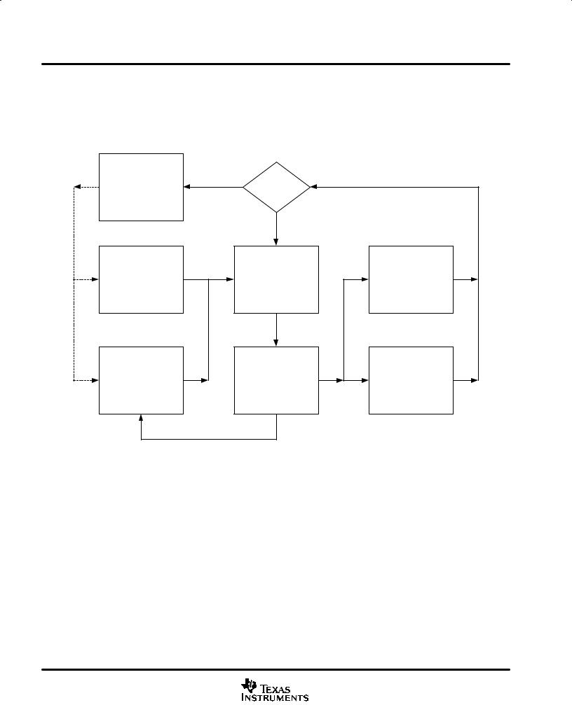
state diagram
A logic state diagram for the UCC397x family of controllers is shown in Figure 5. During power-up the controller transitions from UVLO to the momentary startup state. During startup, the COMP pin is preconditioned at maximum frequency and the OPEN/SD capacitor is discharged before beginning normal operation. In the normal operating state, the frequency is swept from high to low allowing the lamp to be struck and the current in the lamp to be regulated.
ERROR |
|
|
|
|
SHUTDOWN |
YES |
COUNT=7? |
Increment COUNT |
|
|
|
|
|
|
OSC active |
|
|
|
|
OUT off state |
|
|
|
|
|
|
|
* Momentary states |
|
|
|
NO |
|
|
UVLO |
|
STARTUP * |
NO–LOCK * |
|
|
|
|
||
VDD < 3.0V |
VDD>3.0V |
OPEN/SD = 0V |
COMP > 2.5V |
|
OSC inactive |
|
|
||
|
COMP = 0V |
OPEN/SD < 1.5V |
|
|
OUT off state |
|
|
||
|
OSC, OUT active |
OSC, OUT active |
|
|
COUNT=0 |
|
|
||
|
|
|
|
|
SHUTDOWN |
|
|
|
|
OPEN/SD > 2.5V |
|
NORMAL OPERATION |
OPEN LAMP * |
|
COUNT =0 |
|
|
|
|
OSC inactive |
|
OPEN/SD < 1.5V |
1.5V < OPEN/SD <2.5V |
|
OUT off state |
OPEN/SD |
COMP < 2.5V |
COMP < 2.5V |
|
Low current VDD, |
< 0.5V |
OSC, OUT active |
OSC, OUT active |
|
OPEN/SD |
|
|
|
|
|
|
|
OUT off state |
|
|
|
|
UCC3975: OUT1 low, OUT2 low |
|
|
|
|
UCC3976: OUTP high, OUTN high |
|
|
|
|
UCC3977: OUT1 low, OUT2 low |
UDG–01102 |
Figure 5. State Diagram
The normal operating state can be exited in one of four ways:
•bringing VDD < 3 V
•a user commanded shutdown (OPEN/SD > 2.5 V)
•an open lamp condition (OPEN/SD > 1.5 V), or
•if the device fails to achieve regulation before reaching minimum frequency (EAO > 2.5 V).
The latter two conditions cause an internal retry counter to increment before attempting another startup. If the application does not operate normally after seven retrys, the controller enters an error induced shutdown state removing power to the load. The error state and counter can be cleared by removing VDD to the part or by a user commanded shutdown.
8 |
www.ti.com |
UCC2975, UCC2976, UCC2977
UCC3975, UCC3976, UCC3977
SLUS499A – NOVEMBER 2001 – REVISED JANUARY 2002
APPLICATION INFORMATION
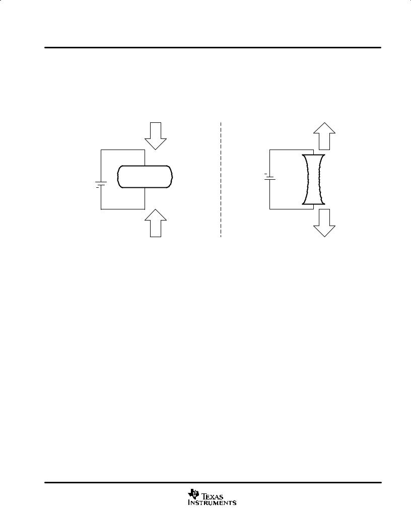
PZT operation
Ceramic piezoelectric transformers were first proposed by C.A. Rosen in 1956. Unlike magnetic transformers that rely on electromagnetic energy transfer, PZTs transfer electric potential to mechanical force as shown in Figure 6. The electrical-to-mechanical conversion of energy is referred to as the reverse piezoelectric effect whereas the mechanical-to-electrical energy conversion is referred to as the direct piezoelectric effect.
ELECTRIC + |
MECHANICAL |
ELECTRIC |
|
MECHANICAL |
FORCE |
POTENTIAL |
+ |
FORCE |
|
POTENTIAL |
|
|
|
|
|
|
|
|
UDG–01099
Figure 6. Piezoelectric Effect
Each manufacturer has a unique recipe of materials and structural layering that determine their PZT’s operating characteristics. Common materials used to make PZTs include lead zirconate, lead titanate and lithium niobate. Single layer PZTs are less costly and easier to manufacture, but have a lower voltage gain (typically 5 to 10 ) and may require a step-up magnetic transformer in order to operate the lamp. Multi-layered PZT designs are more difficult to manufacture, but have a higher voltage gain (20 to 70) allowing a CCFL to be driven using conventional off-the-shelf inductors.
www.ti.com |
9 |
 Loading...