


Texas Instruments UCC3895QTR, UCC3895N, UCC3895DWTR, UCC3895DW, UCC2895QTR Datasheet
...
application
INFO
available
UCC1895
UCC2895
UCC3895
BiCMOS Advanced Phase Shift PWM Controller
FEATURES
•Programmable Output Turn-on Delay
•Adaptive Delay Set
•Bidirectional Oscillator Synchronization
•Capability for Voltage Mode or Current Mode Control
•Programmable Soft Start/Soft Stop and Chip Disable via a Single Pin
•0% to 100% Duty Cycle Control
•7MHz Error Amplifier
•Operation to 1MHz
•Low Active Current Consumption (5mA Typical @ 500kHz)
•Very Low Current Consumption
During Undervoltage Lock-out (150 A typical)
DESCRIPTION
The UCC3895 is a phase shift PWM controller that implements control of a full-bridge power stage by phase shifting the switching of one half-bridge with respect to the other. It allows constant frequency pulse-width modulation in conjunction with resonant zero-voltage switching to provide high efficiency at high frequencies. The part can be used either as a voltage mode or current mode controller.
While the UCC3895 maintains the functionality of the UC3875/6/7/8 family and UC3879, it improves on that controller family with additional features such as enhanced control logic, adaptive delay set, and shutdown capability. Since it is built in BCDMOS, it operates with dramatically less supply current than it’s bipolar counterparts. The UCC3895 can operate with a maximum clock frequency of 1MHz.
The UCC3895 and UCC2895 are offered in the 20 pin SOIC (DW) package, 20 pin PDIP (N) package, 20 pin TSSOP (PW) package, and 20 pin PLCC (Q). The UCC1895 is offered in the 20 pin CDIP (J) package, and 20 pin CLCC package (L).
SIMPLIFIED APPLICATION DIAGRAM
|
UCC3895 |
|
|
Q1 |
|
|
|
|
|
|
|
1 |
EAN |
EAP |
207 |
|
VOUT |
|
|
|
|
|
|
2 |
EAOUT |
SS/DISB |
19 |
|
|
3 |
RAMP |
OUTA |
18 |
|
|
4 |
REF |
OUTB |
17 |
A |
C |
|
|
|
|
||
5 |
GND |
PGND |
16 |
|
VIN |
|
|
|
|
|
|
6 |
SYNC |
VCC |
15 |
VBIAS |
|
7 |
CT |
OUTC |
14 |
B |
D |
|
|
|
|
||
8 |
RT |
OUTD |
13 |
|
|
9 |
DELAB |
CS |
12 |
|
|
10 |
DELCD |
ADS |
11 |
|
|
|
|
|
|
|
UDG-98139 |
SLUS157A - DECEMBER 1999 |
|
|
|
|
|
ABSOLUTE MAXIMUM RATINGS
Supply Voltage (IDD < 10mA) . . . . . . . . . . . . . . . . . . . . . . . 17V Supply Current . . . . . . . . . . . . . . . . . . . . . . . . . . . . . . . . . 30mA REF current . . . . . . . . . . . . . . . . . . . . . . . . . . . . . . . . . . . 15mA OUT Current . . . . . . . . . . . . . . . . . . . . . . . . . . . . . . . . . . 100mA Analog inputs
(EAP, EAN, EAOUT, RAMP,
SYNC, ADS, CS, SS/DISB) . . . . . . . . . . . –0.3V to REF+0.3V Power Dissipation at TA=+25°C (N Package). . . . . . . . . . . . 1W Power Dissipation at TA=+25°C (D Package) . . . . . . . . 650mW Storage Temperature . . . . . . . . . . . . . . . . . . . –65°C to +150°C Junction Temperature. . . . . . . . . . . . . . . . . . . –55°C to +125°C Lead Temperature (soldering, 10 sec). . . . . . . . . . . . . . +300°C
Currents are positive into, negative out of the specified terminal. Consult Packaging Section of Databook for thermal limitations and considerations of package.
TEMPERATURE & PACKAGE SELECTION TABLE
|
TEMPERATURE |
PACKAGE |
|
RANGE |
SUFFIX |
UCC1895 |
–55°C to +125°C |
J, L |
UCC2895 |
–40°C to +85°C |
DW, N, PW, Q |
UCC3895 |
0°C to +70°C |
DW, N, PW, Q |
ORDERING INFORMATION
UCC
 895
895
UCC1895
UCC2895
UCC3895
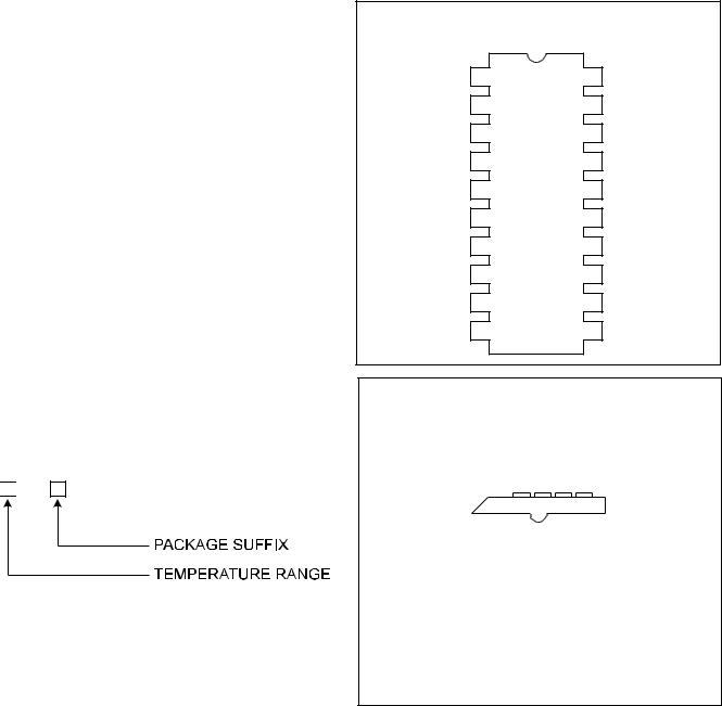
CONNECTION DIAGRAMS
DIL-20,c SOIC-20, TSSOP-20 (TOP VIEW) J or N Package, DW Package, PW Package
EAN |
1 |
20 |
EAP |
EAOUT |
2 |
19 |
SS/DISB |
RAMP |
3 |
18 |
OUTA |
REF |
4 |
17 |
OUTB |
GND |
5 |
16 |
PGND |
SYNC |
6 |
15 |
VDD |
CT |
7 |
14 |
OUTC |
RT |
8 |
13 |
OUTD |
DELAB |
9 |
12 |
CS |
DELCD |
10 |
11 |
ADS |
PLCC-20, CLCC-20 (TOP VIEW)
Q Package, L Package
EAN |
|
|
|
|
|
|
|
|
|
|
|
|
|
|
|
|
|
|
|
|
|
|
|
|
|
|
|
|
|
|
|
|
|
|
|
|
|
|
|
|
|
|
|
|
|
|
|
|
|
|
|
|
|
|
|
|
|
|
|
|
|
|
|
|
|
|
|
|
|
|
|
|
|
|
|
||
EAOUT |
|
|
|
|
|
|
|
|
|
|
|
|
|
|
|
|
|
|
|
|
|
|
|
|
|
|
|
|
|
|
|
|
|
|
|
|
EAP |
|
|
|
|
|
|
|
|
|
|
|
|
|
|
|
|
|
|
|
|
|
|
|
|
|
|
|
|
|
|
|
|
|
|
|
|
|
|||
RAMP |
|
|
|
|
|
|
|
|
|
|
|
|
|
|
|
|
|
|
|
|
|
|
|
|
|
|
|
|
|
|
|
|
|
|
|
|
SS/DISB |
|
|
|
|
|
|
|
|
|
|
|
|
|
|
|
|
|
|
|
|
|
|
|
|
|
|
|
|
|
|
|
|
|
|
|
|
|
|||
|
|
|
|
|
|
|
|
|
|
|
|
|
|
|
|
|
|
|
|
|
|
|
|
|
|
|
|
|
|
|
|
|
|
|
|
|
|
|
|
|
|
|
|
|
|
3 |
|
|
|
2 |
1 |
20 |
19 |
|
|
|
|||||||||||||||||||||
REF |
|
|
4 |
|
|
|
|
|
|
|
|
|
|
|
|
|
|
|
|
|
|
|
|
|
|
|
|
|
|
18 |
|
|
OUTA |
|||||
|
|
|
|
|
|
|
|
|
|
|
|
|
|
|
|
|
|
|
|
|
|
|
|
|
|
|
|
|
|
|||||||||
|
|
|
|
|
|
|
|
|
|
|
|
|
|
|
|
|
|
|
|
|
|
|
|
|
|
|
|
|
|
|||||||||
GND |
|
|
5 |
|
|
|
|
|
|
|
|
|
|
|
|
|
|
|
|
|
|
|
|
|
|
|
|
|
|
17 |
|
|
OUTB |
|||||
|
|
|
|
|
|
|
|
|
|
|
|
|
|
|
|
|
|
|
|
|
|
|
|
|
|
|
|
|
|
|||||||||
|
|
|
|
|
|
|
|
|
|
|
|
|
|
|
|
|
|
|
|
|
|
|
|
|
|
|
|
|
|
|||||||||
|
|
|
|
|
|
|
|
|
|
|
|
|
|
|
|
|
|
|
|
|
|
|
|
|
|
|
|
|
|
|||||||||
SYNC |
|
|
6 |
|
|
|
|
|
|
|
|
|
|
|
|
|
|
|
|
|
|
|
|
|
|
|
|
|
|
16 |
|
|
PGND |
|||||
|
|
|
|
|
|
|
|
|
|
|
|
|
|
|
|
|
|
|
|
|
|
|
|
|
|
|
|
|
|
|||||||||
|
|
|
|
|
|
|
|
|
|
|
|
|
|
|
|
|
|
|
|
|
|
|
|
|
|
|
|
|
|
|||||||||
|
|
|
|
|
|
|
|
|
|
|
|
|
|
|
|
|
|
|
|
|
|
|
|
|
|
|
|
|
|
|||||||||
CT |
|
|
7 |
|
|
|
|
|
|
|
|
|
|
|
|
|
|
|
|
|
|
|
|
|
|
|
|
|
|
15 |
|
|
VDD |
|||||
|
|
|
|
|
|
|
|
|
|
|
|
|
|
|
|
|
|
|
|
|
|
|
|
|
|
|
|
|
|
|||||||||
|
|
|
|
|
|
|
|
|
|
|
|
|
|
|
|
|
|
|
|
|
|
|
|
|
|
|
|
|
|
|||||||||
|
|
|
|
|
|
|
|
|
|
|
|
|
|
|
|
|
|
|
|
|
|
|
|
|
|
|
|
|
|
|||||||||
RT |
|
|
8 |
|
|
|
|
|
|
|
|
|
|
|
|
|
|
|
|
|
|
|
|
|
|
|
|
|
|
14 |
|
|
OUTC |
|||||
|
|
|
|
|
|
|
|
|
|
|
|
|
|
|
|
|
|
|
|
|
|
|
|
|
|
|
|
|
|
|||||||||
|
|
|
|
|
|
|
|
|
|
|
|
|
|
|
|
|
|
|
|
|
|
|
|
|
|
|
|
|
|
|||||||||
|
|
|
|
|
|
|
|
|
|
|
|
|
|
|
|
|
|
|
|
|
|
|
|
|
|
|
|
|
|
|||||||||
DELAB |
|
|
9 |
|
|
|
10 |
11 |
12 |
|
|
13 |
|
|
|
|
OUTD |
|||||||||||||||||||||
|
|
|
|
|||||||||||||||||||||||||||||||||||
|
|
|
|
|
|
|
|
|
|
|
|
|
|
|
|
|
|
|
|
|
|
|
|
|
|
|
|
|
|
|
|
|
|
|
|
|||
|
|
|
|
|
|
|
|
|
|
|
|
|
|
|
|
|
|
|
|
|
|
|
|
|
|
|
|
|
|
|
|
|
|
|
|
|||
DELCD |
|
|
|
|
|
|
|
|
|
|
|
|
|
|
|
|
|
|
|
|
|
|
|
|
|
|
|
|
|
|
|
|
|
|
|
|
CS |
|
|
|
|
|
|
|
|
|
|
|
|
|
|
|
|
|
|
|
|
|
|
|
|
|
|
|
|
|
|
|
|
|
|
|
|
|
|||
|
|
|
|
|
|
|
|
|
|
|
|
|
|
|
|
|
|
|
|
|
|
|
|
|
|
|
|
|
|
|
|
|
|
|
|
|
|
ADS |
|
|
|
|
|
|
|
|
|
|
|
|
|
|
|
|
|
|
|
|
|
|
|
|
|
|
|
|
|
|
|
|
|
|
|
|
|
|
|
ELECTRICAL CHARACTERISTICS: Unless otherwise specified, VDD=12V, RT=82kΩ, CT=220pF, RDELAB=10kΩ,
RDELCD=10kΩ, CREF=0.1 F, CVDD=1.0 F, no load at outputs. TA = TJ. TA = 0°C to 70°C for UCC3895x, –40°C to +85°C for UCC2895x, and –55°C to +125°C for UCC1895x.
PARAMETER |
TEST CONDITIONS |
MIN |
TYP |
MAX |
UNITS |
UVLO Section |
|
|
|
|
|
Start Threshold |
|
10.2 |
11 |
11.8 |
V |
Stop Threshold |
|
8.2 |
9 |
9.8 |
V |
Hysteresis |
|
1.0 |
2.0 |
3.0 |
V |
Supply Current |
|
|
|
|
|
Start-up Current |
VDD = 8V |
|
150 |
250 |
A |
IDD Active |
|
|
5 |
6 |
mA |
VDD Clamp Voltage |
IDD = 10mA |
16.5 |
17.5 |
18.5 |
V |
2
UCC1895
UCC2895
UCC3895
ELECTRICAL CHARACTERISTICS: Unless otherwise specified, VDD=12V, RT=82kΩ, CT=220pF, RDELAB=10kΩ,
RDELCD=10kΩ, CREF=0.1 F, CVDD=1.0 F, no load at outputs. TA = TJ. TA = 0°C to 70°C for UCC3895x, –40°C to +85°C for UCC2895x, and –55°C to +125°C for UCC1895x.
PARAMETER |
TEST CONDITIONS |
MIN |
TYP |
MAX |
UNITS |
Voltage Reference Section |
|
|
|
|
|
Output Voltage |
TJ = 25°C |
4.94 |
5.00 |
5.06 |
V |
|
10V < VDD < 17.5V, 0mA < IREF < 5mA, |
4.85 |
5 |
5.15 |
V |
|
Temperature |
|
|
|
|
Short Circuit Current |
REF = 0V, TJ = 25°C |
10 |
20 |
|
mA |
Error Amplifier Section |
|
|
|
|
|
Common Mode Input Voltage Range |
|
–0.1 |
|
3.6 |
V |
Offset Voltage |
|
–7 |
|
7 |
mV |
Input Bias Current (EAP, EAN) |
|
–1 |
|
1 |
A |
EAOUT VOH |
EAP–EAN = 500mV, IEAOUT= –0.5mA |
4.0 |
4.5 |
5.0 |
V |
EAOUT VOL |
EAP–EAN = –500mV, IEAOUT= 0.5mA |
0 |
0.2 |
0.4 |
V |
EAOUT Source Current |
EAP–EAN = 500mV, EAOUT= 2.5V |
1.0 |
1.5 |
|
mA |
EAOUT Sink Current |
EAP–EAN = –500mV, EAOUT= 2.5V |
2.5 |
4.5 |
|
mA |
Open Loop DC Gain |
|
75 |
85 |
|
dB |
Unity Gain Bandwidth |
(Note 3) |
5.0 |
7.0 |
|
MHz |
Slew Rate |
EAN from 1V to 0V, EAP = 500mV, |
1.5 |
2.2 |
|
V/ s |
|
EAOUT from 0.5V to 3.0V |
|
|
|
|
No Load Comparator Turn-Off Threshold |
|
0.45 |
0.50 |
0.55 |
V |
No Load Comparator Turn-On Threshold |
|
0.55 |
0.60 |
0.69 |
V |
No Load Comparator Hysteresis |
|
0.035 |
0.100 |
0.165 |
V |
Oscillator Section |
|
|
|
|
|
Frequency |
TJ = 25°C |
473 |
500 |
527 |
kHz |
Total Variation |
Line, Temperature (Note 3) |
|
2.5 |
5 |
% |
SYNC VIH |
|
2.05 |
2.10 |
2.25 |
V |
SYNC VIL |
|
1.85 |
1.90 |
1.95 |
V |
SYNC VOH |
ISYNC = –400 A, CT = 2.6V |
4.1 |
4.5 |
5.0 |
V |
SYNC VOL |
ISYNC = 100 A, CT = 2.6V |
0.0 |
0.5 |
1.0 |
V |
SYNC Output Pulse Width |
SYNC Load = 3.9kΩ and 30pF in parallel |
|
85 |
135 |
ns |
RT Voltage |
|
2.9 |
3 |
3.1 |
V |
CT Peak Voltage |
|
2.25 |
2.35 |
2.50 |
V |
CT Valley Voltage |
|
0.0 |
0.2 |
0.4 |
V |
PWM Comparator Section |
|
|
|
|
|
EAOUT to RAMP Input Offset Voltage |
RAMP = 0V, DELAB = DELCD = REF |
0.72 |
0.85 |
1.05 |
V |
Minimum Phase Shift |
RAMP = 0V, EAOUT = 650mV (Note 1) |
0.00 |
0.85 |
1.40 |
% |
(OUTA to OUTC, OUTB to OUTD) |
|
|
|
|
|
RAMP to OUTC/OUTD Delay |
RAMP from 0V to 2.5V, EAOUT = 1.2V, |
|
70 |
120 |
ns |
|
DELAB = DELCD = REF (Note 2) |
|
|
|
|
RAMP Bias Current |
RAMP < 5V, CT < 2.2V |
–5 |
|
5 |
A |
RAMP Sink Current |
RAMP = 5V, CT < 2.6V |
12 |
19 |
|
mA |
Current Sense Section |
|
|
|
|
|
CS Bias Current |
0 < CS , 2.5V, 0 < ADS < 2.5V |
–4.5 |
|
20 |
A |
Peak Current Threshold |
|
1.90 |
2.00 |
2.10 |
V |
Overcurrent Threshold |
|
2.4 |
2.5 |
2.6 |
V |
CS to Output Delay |
CS from 0 to 2.3V, DELAB = DELCD = REF |
|
75 |
110 |
ns |
3
 Loading...