


Texas Instruments UC3827DW-1, UC3827Q-1, UC3827N-1, UC3827N-2, UC3827DWTR-1 Datasheet
...
UC1827-1/-2
UC2827-1/-2
UC3827-1/-2
Buck Current/Voltage Fed Push-Pull PWM Controllers
FEATURES
∙Ideal for Multiple Output and/or High Voltage Output Voltage Converters
∙Up to 500kHz Operation
∙High Voltage, High Current Floating Driver for Buck Converter Stage
∙UC3827-1 Current Fed Controller has Push-Pull Drivers with Overlapping Conduction Periods
∙UC3827-2 Voltage Fed Controller has Push-Pull Drivers with Non-overlapping Conduction Periods
∙Average Current Mode, Peak Current Mode or Voltage Mode with Input Voltage Feedforward Control for Buck Power Stage
∙Wide Bandwidth, Low Offset, Differential Current Sense Amplifier
∙Precise Short Circuit Current Control
DESCRIPTION
The UC3827 family of controller ICs provides an integrated control solution for cascaded buck and push-pull converters. These converters are known as current fed or voltage fed push-pull converters and are ideally suited for multiple output and/or high voltage output applications. In both current fed and voltage fed modes, the push-pull switches are driven at 50% nominal duty cycles and at one half the switching frequency of the buck stage. In the current fed mode, the two switches are driven with a guaranteed overlap period to prevent ringing and voltage stress on the devices. In the voltage fed mode, the two switches are driven with a guaranteed gap time between the switches to prevent shorting the transformer across the energy storage capacitor and to prohibit excessive currents flowing through the devices.
The converter’s output voltage is regulated by pulse width modulation of the buck switch. The UC3827 contains complete protection and PWM control functions for the buck converter. Easy control of the floating switch is accomplished by the floating drive circuitry. The gate drive waveform is level shifted to support an input voltage up to 72Vdc.
(continued)
BLOCK DIAGRAM
|
|
|
|
VEAO |
CEA+ |
CEAO |
RAMP |
|
|
|
|
|
|
|
|
|
10 |
12 |
6 |
5 |
|
|
|
|
|
|
|
VOLTAGE ERROR |
|
|
|
|
|
|
|
|
|
|
|
|
AMPLIFIER |
|
|
|
|
|
|
|
|
|
|
VEA+ |
14 |
|
|
|
|
|
|
|
|
|
|
|
|
|
|
|
|
CURRENT |
|
0.7V |
|
|
|
|
|
VEA– |
16 |
|
|
|
ERROR |
|
|
|
|
|
|
|
|
|
|
|
|
|
|
|
|
|
|||
|
|
|
|
|
AMPLIFIER |
|
|
|
|
|
|
|
CEA– |
13 |
|
|
|
|
|
|
|
|
|
|
|
|
|
|
|
|
|
|
PWM |
RD |
|
|
|
|
CSAO |
7 |
|
|
|
|
|
COMPARATOR |
|
FLYING |
1 |
V+ |
|
|
|
|
|
|
|
|
|
|
|
|||
|
|
|
|
+3V |
|
|
|
|
|
DRIVER |
||
CSA+ |
8 |
|
|
|
|
|
|
|
|
|
||
|
|
ILIM |
|
|
|
S |
Q |
|
2 |
BUCK |
||
|
|
|
|
|
|
|
|
|||||
|
|
|
|
|
|
|
|
|
|
|||
CSA– |
9 |
CURRENT |
COMPARATOR |
|
|
|
|
|
|
|
||
|
|
|
|
|
|
|
3 |
SRC |
||||
|
|
SENSE AMPLIFIER |
|
|
|
|
|
|
||||
SS |
4 |
|
|
|
SS |
|
|
OSC |
|
|
|
|
|
|
|
|
|
|
|
|
|
|
|||
|
|
|
|
|
INHBT |
|
|
|
|
|
|
|
SYNC |
19 |
|
|
|
UV |
|
|
|
|
|
21 |
PGND |
|
|
|
|
|
|
|
|
|
|
|
|
|
CT |
18 |
OSC |
|
|
|
|
Q |
DELAY |
|
|
|
|
|
|
|
|
|
|
|
|
|
|
|||
RT |
17 |
500kHz |
|
|
|
|
T |
|
|
PUSH-PULL |
|
|
MAX |
|
|
|
|
Q |
|
|
|
|
|||
|
|
|
|
|
|
DRIVERS |
|
|
||||
|
|
|
|
|
|
|
|
|
|
|
||
REF |
15 |
|
|
|
|
|
|
|
|
|
24 |
PUSH |
|
|
|
|
|
|
|
|
|
|
|
||
VCC |
23 |
REF |
|
|
|
|
|
|
|
|
|
|
|
|
|
|
|
|
|
|
|
|
|
|
|
|
|
& |
UVLO |
|
|
|
DELAY |
|
|
22 |
PULL |
|
GND |
11 |
UVLO |
|
|
|
|
|
|||||
|
|
|
|
|
|
|
|
|
|
|||
|
|
|
|
|
|
|
|
|
|
|
||
|
|
|
|
|
|
|
|
20 |
|
|
|
|
|
|
|
|
|
|
|
|
DELAY |
|
|
UDG-97172 |
|
04/99 |
|
|
|
|
|
|
|
|
|
|
|
|
DESCRIPTION (cont.)
The UC3827 can be set up in traditional voltage mode control using input voltage feedforward technique or in current mode control. Using current mode control prevents potential core saturation of the push-pull transformer due to mismatches in timing and in component tolerances. With average current mode control, precise control of the inductor current feeding the push-pull stage is possible without the noise sensitivity associated with peak current mode control. The UC3827 average current mode loop can also be connected in parallel with the voltage regulation loop to assist only in fault conditions.
Other valuable features of the UC3827 include bidirectional synchronization capability, user programmable overlap time (UC3827-1), user programmable gap time (UC3827-2), a high bandwidth differential current sense amplifier, and soft start circuitry.
ABSOLUTE MAXIMUM RATINGS
Supply Voltage, VCC. . . . . . . . . . . . . . . . . . . . . . . . . . . . . . 20V Input Voltage Range
For all pins except V+, BUCK, SRC . . . . . . . . . . –0.3V to 5V For V+ and BUCK. . . . . . . . . . . . . . . . . . . . . . . . . . . . . . 90V For SRC . . . . . . . . . . . . . . . . . . . . . . . . . . . . . . . . 90V–VCC
BUCK Driver
IO Continuous. . . . . . . . . . . . . . . . . . . . . . . . . . . . . ± 250mA IO Peak . . . . . . . . . . . . . . . . . . . . . . . . . . . . . . . . . . . . . ± 1A
PUSH/PULL Driver
IO Continuous. . . . . . . . . . . . . . . . . . . . . . . . . . . . . ± 200mA IO Peak. . . . . . . . . . . . . . . . . . . . . . . . . . . . . . . . . . . . ± 0.8A Storage Temperature . . . . . . . . . . . . . . . . . . . −65°C to +150°C Junction Temperature. . . . . . . . . . . . . . . . . . . –55°C to +150°C Lead Temperature (Soldering, 10 sec.) . . . . . . . . . . . . . +300°C
Voltages are referenced to ground. Currents are positive into, negative out of the specified terminal. Consult Packaging Section of Databook for thermal limitations and considerations of packages.
TEMPERATURE AND PACKAGE
SELECTION GUIDE
|
TEMPERATURE |
AVAILABLE |
|
RANGE |
PACKAGES |
UC1827-X |
–55°C to +125°C |
J |
UC2827-X |
–40°C to +85°C |
N, DW, Q |
UC3827-X |
0°C to +70°C |
N, DW, Q |
UC1827-1/-2
UC2827-1/-2
UC3827-1/-2
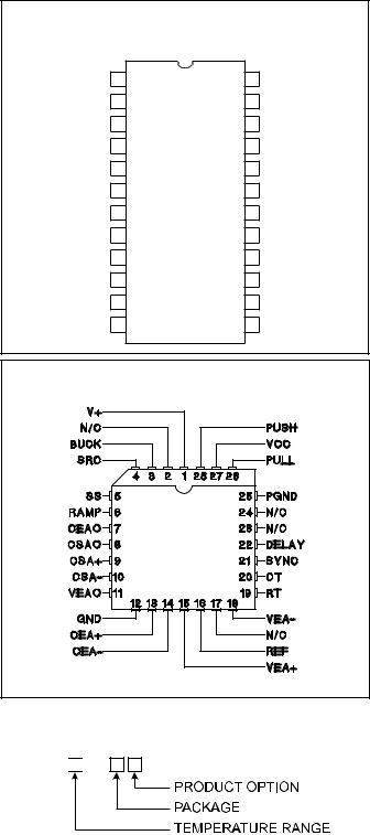
CONNECTION DIAGRAMS
DIL-24 (Top View)
N or J, DW Packages
V+ |
1 |
24 |
PUSH |
BUCK |
2 |
23 |
VCC |
SRC |
3 |
22 |
PULL |
SS |
4 |
21 |
PGND |
RAMP |
5 |
20 |
DELAY |
CEAO |
6 |
19 |
SYNC |
CSAO |
7 |
18 |
CT |
CSA+ |
8 |
17 |
RT |
CSA– |
9 |
16 |
VEA– |
VEAO |
10 |
15 |
REF |
GND |
11 |
14 |
VEA+ |
CEA+ |
12 |
13 |
CEA– |
PLCC-28 (Top View)
Q Package
ORDERING INFORMATION
UC 
 827
827
PART VERSION GUIDE
PART NUMBER |
TOPOLOGY |
UCX827-1 |
Current Fed Push-Pull |
UCX827-2 |
Voltage Fed Push-Pull |
2
UC1827-1/-2
UC2827-1/-2
UC3827-1/-2
ELECTRICAL CHARACTERISTICS Unless otherwise specified, VCC = 15V, V+ = 14.3V, CT = 340pF, RT = 10K, RDELAY = 24.3k, SRC = GND, BUCK, PUSH and PULL outputs no load. TJ = TA.
PARAMETER |
TEST CONDITIONS |
MIN |
TYP |
MAX |
UNITS |
Supply |
|
|
|
|
|
VCC UVLO, Turn-On |
|
8.3 |
8.8 |
9.5 |
V |
Hysteresis |
|
0.9 |
1.2 |
1.5 |
V |
IVCC Start |
VCC = 8V |
|
|
1000 |
μA |
IVCC Run |
|
|
32 |
45 |
mA |
V+ UVLO, Turn-On |
|
7.1 |
7.5 |
8.3 |
V |
V+ Hysteresis |
|
0.2 |
0.4 |
0.9 |
V |
IV+ Buck High |
|
0.2 |
1 |
2 |
mA |
Voltage Error Amplifier |
|
|
|
|
|
IB |
|
|
0.5 |
3 |
μA |
VIO |
|
|
|
10 |
mV |
AVOL |
|
80 |
95 |
|
dB |
GBW |
(Note 7) |
1 |
4 |
|
MHz |
VOL |
IVEAO = 0μA (No Load) |
|
0.3 |
0.5 |
V |
VOH |
IVEAO = 0μA (No Load) |
2.85 |
3 |
3.20 |
V |
Current Sense Amplifier |
|
|
|
|
|
IB |
|
|
–1 |
–5 |
uA |
VIO |
|
|
|
5 |
mV |
AVOL |
|
80 |
110 |
|
dB |
GBW |
(Note 7) |
15 |
29 |
|
MHz |
VOL |
ICEAO = 0μA (No Load) |
|
0.25 |
0.5 |
V |
VOH |
ICEAO = 0μA (No Load) |
3 |
3.3 |
|
V |
Common Mode Range |
(Note 7) |
0 |
|
2 |
V |
Current Error Amplifier |
|
|
|
|
|
IB |
|
|
–1 |
–5 |
μA |
VIO |
|
|
|
10 |
mV |
AVOL |
|
80 |
110 |
|
dB |
GBW |
At 100kHz, Measure Gain |
2 |
4.5 |
|
MHz |
VOL |
ICEAO = 0μA (No Load) |
|
0.25 |
0.5 |
V |
VOH |
ICEAO = 0μA (No Load) |
3.3 |
3.5 |
|
V |
Common Mode Range |
(Note 7) |
0 |
|
5 |
V |
Oscillator Section |
|
|
|
|
|
Frequency |
|
180 |
220 |
250 |
kHz |
CT Discharge Current |
3.5V at CT when CT removed |
5 |
|
|
mA |
PWM Comparator |
|
|
|
|
|
Minimum Duty Cycle |
200kHz |
|
|
0 |
% |
Maximum Duty Cycle |
200kHz |
85 |
91 |
95 |
% |
Buck Output Stage |
|
|
|
|
|
Rise Time |
1nF Load, (Note 3) |
|
40 |
100 |
ns |
Fall Time |
1nF, Load |
|
30 |
80 |
ns |
VOH |
IBUCK = –15mA , V+ –BUCK (Note 4) |
|
1.5 |
2.5 |
V |
|
IBUCK = –150mA, V+ – BUCK (Note 4) |
|
2 |
2.5 |
V |
VOL |
IBUCK = 15mA (Note 5) |
|
0.2 |
0.4 |
V |
|
IBUCK = 150mA (Note 5) |
|
0.7 |
1.2 |
V |
3
 Loading...