


Texas Instruments UC3853N, UC3853DTR, UC3853D, UC2853N, UC2853D Datasheet
...
UC1853
UC2853
UC3853
High Power Factor Preregulator
FEATURES
∙Complete 8-pin Power Factor Solution
∙Reduced External Components
∙RMS Line Voltage Compensation
∙Precision Multiplier/Squarer/Divider
∙Internal 75kHz Synchronizable Oscillator
∙Average Current Mode PWM Control
∙Overvoltage Protection Comparator
∙High Current, Clamped Gate Driver
DESCRIPTION
The UC3853 provides simple, yet high performance active power factor correction. Using the same control technique as the UC1854, this 8-pin device exploits a simplified architecture and an internal oscillator to minimize external component count. The UC3853 incorporates a precision multiplier/squarer/divider circuit, voltage and current loop error amplifiers, and a precision voltage reference to implement average current mode control with RMS line voltage compensation. This control technique maintains constant loop gain with changes in input voltage, which minimizes input line current distortion over the worldwide input voltage range.
The internal 75kHz oscillator includes an external clock input, allowing synchronization to downstream converters. Additionally, the device features an overvoltage protection comparator, a clamped MOSFET gate driver which self-biases low during undervoltage lockout, and low startup and supply current.
These devices are available in 8-pin plastic and ceramic dual in-line (DIP) packages, and 8-lead small outline (SOIC) packages. The UC1853 is specified for operation from –55°C to +125°C, the UC2853 is specified for operation from –25°C to +85°C, and the UC3853 is specified for operation from 0°C to +70°C.
BLOCK DIAGRAM
UDG-94120-1 |
11/97 |
ABSOLUTE MAXIMUM RATINGS
Supply Voltage (VCC) . . . . . . . . . . . . . . . . . . . . . . . . . . . . . 40V Output Drive Current,
Continuous . . . . . . . . . . . . . . . . . . . . . . . . . . . . . . . . 0.125A Peak . . . . . . . . . . . . . . . . . . . . . . . . . . . . . . . . . . . . . . . 0.5A Output Minimum Voltage . . . . . . . . . . . . . . . . . . . . . . . . . –0.3V IAC Maximum Input Current . . . . . . . . . . . . . . . . . . . . . . . . 1mA IMO Maximum Output Current . . . . . . . . . . . . . . . . . . . . . –2mA IMO Minimum Voltage . . . . . . . . . . . . . . . . . . . . . . . . . . . –0.3V FB Maximum Input Voltage . . . . . . . . . . . . . . . . . . . . . . . . . . 5V VCOMP Maximum Voltage. . . . . . . . . . . . . . . . . . . . . . . . . 6.2V ICOMP Sourcing Current . . . . . . . . . . . . . . . . . . . . Self-Limiting ICOMP Sinking Current . . . . . . . . . . . . . . . . . . . . . . . . . . 20mA ICOMP Maximum Voltage . . . . . . . . . . . . . . . . . . . . . . . . . 7.2V Storage Temperature . . . . . . . . . . . . . . . . . . . –65°C to +150°C Junction Temperature. . . . . . . . . . . . . . . . . . . –55°C to +150°C Lead Temperature (Soldering, 10 sec.) . . . . . . . . . . . . . +300°C
All voltages with respect to GND. Currents are positive into, negative out of the specified terminal. Consult Packaging Section of Databook for thermal limitations and considerations of packages.
UC1853
UC2853
UC3853
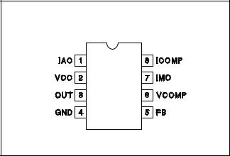
CONNECTION DIAGRAM
DIL-8, SOIC-8 (Top View)
J or N, D Package
ELECTRICAL CHARACTERISTICS |
Unless otherwise stated, these parameters apply for TA = –55°C to +125°C for the |
||||
|
UC1853; –25°C to +85°C for the 2853; and 0°C to +70°C for the UC3853; VCC = |
||||
|
16V, VFB = 3V, IAC = 100mA, VVCOMP = 3.75V, VICOMP = 3V, TA = TJ. |
|
|||
PARAMETER |
TEST CONDITIONS |
MIN |
TYP |
MAX |
UNITS |
Undervoltage Lockout Section |
|
|
|
|
|
VCC Turn-on Threshold |
VVCOMP, VICOMP Open |
|
11.5 |
13 |
V |
Hysteresis |
|
1.5 |
1.8 |
2.1 |
V |
Supply Current Section |
|
|
|
|
|
IVCC Startup |
VCC = 8V, IAC = 100μA; VVCOMP, VICOMP Open |
|
250 |
500 |
mA |
IVCC |
IAC = 0μA, VICOMP = 0V |
|
10 |
15 |
mA |
Voltage Loop Error Amplifier Section |
|
|
|
|
|
Transconductance |
IOUT = ± 20μA 0-70C |
300 |
450 |
575 |
μmho |
|
Temperature |
135 |
|
640 |
μmho |
Input Voltage |
0-70C |
2.925 |
3 |
3.075 |
V |
|
Temperature |
2.9 |
|
3.1 |
V |
AVOL |
VVCOMP = 1V – 4V |
50 |
60 |
|
dB |
Output Sink Current |
VFB = 3.2V, VVCOMP = 3.75V |
20 |
50 |
|
μA |
Output Source Current |
VFB = 2.8V, VVCOMP = 3.75V |
|
–50 |
–20 |
μA |
Output Voltage High |
|
5.5 |
6 |
|
V |
Output Voltage Low |
|
|
0.6 |
0.9 |
V |
Current Loop Error Amplifier Section |
|
|
|
|
|
Offset Voltage |
|
0 |
|
6 |
mV |
Voltage Gain |
VICOMP = 1V – 4V |
|
70 |
|
dB |
Sink Current |
VIMO = 100mV, VICOMP = 3V |
1 |
|
|
mA |
Source Current |
VIMO = –0.1V, VICOMP = 3V |
|
–150 |
–80 |
mA |
Output High |
IICOMP = –50mA |
6 |
6.8 |
|
V |
Output Low |
IICOMP = 50mA |
|
0.3 |
0.8 |
V |
PWM Modulator Gain |
VICOMP = 2V – 3V (Note 1) |
|
20 |
|
%/V |
2
 Loading...