


Texas Instruments UC3848N, UC3848DWTR, UC3848DW, UC2848DW, UC2848N Datasheet
...
UC1848
UC2848
UC3848
Average Current Mode PWM Controller
FEATURES
∙Practical Primary Side Control of Isolated Power Supplies with DC Control of Secondary Side Current
∙Accurate Programmable Maximum Duty Cycle Clamp
∙Maximum Volt-Second Product Clamp to Prevent Core Saturation
∙Practical Operation Up to 1MHz
∙High Current (2A Pk) Totem Pole Output Driver
∙Wide Bandwidth (8MHz) Current Error Amplifier
∙Under Voltage Lockout Monitors VCC, VIN and VREF
∙Output Active Low During UVLO
∙Low Startup Current (500μA)
∙Precision 5V Reference (1%)
DESCRIPTION
BLOCK DIAGRAM
UDG-93003-1 |
The UC3848 family of PWM control ICs makes primary |
output driver. The current error amplifier easily interfaces |
|
side average current mode control practical for isolated |
with an optoisolator from a secondary side voltage sens- |
|
switching converters. Average current mode control in- |
ing circuit. |
|
sures that both cycle by cycle peak switch current and |
A full featured undervoltage lockout (UVLO) circuit is con- |
|
maximum average inductor current are well defined and |
||
tained in the UC3848. UVLO monitors the supply voltage |
||
will not run away in a short circuit situation. The UC3848 |
||
to the controller (VCC), the reference voltage (VREF), |
||
can be used to control a wide variety of converter topolo- |
||
and the input line voltage (VIN). All three must be good |
||
gies. |
||
before soft start commences. If either VCC or VIN is low, |
||
|
||
In addition to the basic functions required for pulse width |
the supply current required by the chip is only 500μA and |
|
modulation, the UC3848 implements a patented tech- |
the output is actively held low. |
|
nique of sensing secondary current in an isolated buck |
Two on board protection features set controlled limits to |
|
derived converter from the primary side. A current wave- |
||
prevent transformer core saturation. Input voltage is mon- |
||
form synthesizer monitors switch current and simulates |
||
itored and pulse width is constrained to limit the maxi- |
||
the inductor current down slope so that the complete cur- |
||
mum volt-second product applied to the transformer. A |
||
rent waveform can be constructed on the primary side |
||
unique patented technique limits maximum duty cycle |
||
without actual secondary side measurement. This infor- |
||
within 3% of a user programmed value. |
||
mation on the primary side allows for full DC control of |
||
These two features allow for more optimal use of trans- |
||
output current. |
||
The UC3848 circuitry includes a precision reference, a |
formers and switches, resulting in reduced system size |
|
and cost. |
||
wide bandwidth error amplifier for average current con- |
||
Patents embodied in the UC3848 belong to Lambda |
||
trol, an oscillator to generate the system clock, latching |
||
PWM comparator and logic circuits, and a high current |
Electronics Incorporated and are licensed for use in ap- |
|
|
plications employing these devices. |
|
4/96 |
|
ABSOLUTE MAXIMUM RATINGS
Supply Voltage (Pin 15). . . . . . . . . . . . . . . . . . . . . . . . . . . . 22V Output Current, Source or Sink (Pin 14)
DC . . . . . . . . . . . . . . . . . . . . . . . . . . . . . . . . . . . . . . . . . 0.5A Pulse (0.5 s) . . . . . . . . . . . . . . . . . . . . . . . . . . . . . . . . 2.2A Power Ground to Ground (Pin 1 to Pin 13) . . . . . . . . . . . ± 0.2V
Analog Input Voltages
(Pins 3, 4, 7, 8, 12, 16) . . . . . . . . . . . . . . . . . . . . . –0.3 to 7V Analog Input Currents, Source or Sink
(Pins 3, 4, 7, 8, 11, 12, 16) . . . . . . . . . . . . . . . . . . . . . . 1mA
UC1848
UC2848
UC3848
Analog Output Currents, Source or Sink (Pins 5 & 10) . . . 5mA Power Dissipation at TA = 60°C . . . . . . . . . . . . . . . . . . . . . . 1W Storage Temperature Range . . . . . . . . . . . . . . . −65°C to +150 °C Lead Temperature (Soldering 10 seconds) . . . . . . . . . . +300°C
Notes: All voltages are with respect to ground (DIL and SOIC Pin 1). Currents are positive into the specified terminal. Pin numbers refer to the 16 pin DIL and SOIC packages. Consult Packaging Section of Databook for thermal limitations and considerations of packages.
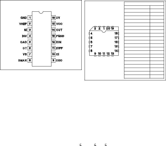
CONNECTION DIAGRAMS
DIL-16, SOIC-16 (Top View) |
PLCC-20 & LCC-20 |
PACKAGE PIN FUNCTION |
|
J, N, or DW Packages |
(Top View) |
FUNCTION |
PIN |
|
N/C |
1 |
|
|
Q & L Packages |
||
|
GND |
2 |
|
|
|
||
|
|
VREF |
3 |
|
|
NI |
4 |
|
|
INV |
5 |
|
|
N/C |
6 |
|
|
CAO |
7 |
|
|
CT |
8 |
|
|
VS |
9 |
|
|
DMAX |
10 |
|
|
N/C |
11 |
|
|
CDC |
12 |
|
|
CI |
13 |
|
|
IOFF |
14 |
|
|
ION |
15 |
|
|
N/C |
16 |
|
|
PGND |
17 |
|
|
OUT |
18 |
|
|
VCC |
19 |
|
|
UV |
20 |
ELECTRICAL CHARACTERISTICS: Unless otherwise stated, all specifications are over the junction temperature range of −55°C to +125°C for the UC1848, −40°C to +85°C for the UC2848, and 0°C to +70°C for the UC3848. Test conditions are: VCC = 12V, CT = 400pF, CI = 100pF, IOFF = 100μA, CDC = 100nF, Cvs = 100pF, and Ivs = 400μA, TA = TJ.
PARAMETER |
TEST CONDITIONS |
MIN |
TYP |
MAX |
UNITS |
Real Time Current Waveform Synthesizer |
|
|
|
|
|
Ion Amplifier |
|
|
|
|
|
Offset Voltage |
|
0.95 |
1 |
1.05 |
V |
Slew Rate (Note 1) |
|
20 |
25 |
|
V/μs |
lib |
|
|
-2 |
-20 |
μA |
IOFF Current Mirror |
|
|
|
|
|
Input Voltage |
|
0.95 |
1 |
1.05 |
V |
Current Gain |
|
0.9 |
1 |
1.1 |
A/A |
Current Error Amplifier |
|
|
|
|
|
AVOL |
|
60 |
100 |
|
dB |
Vio |
12V ≤ VCC 20V, 0V VCM 5V |
|
|
10 |
mV |
lib |
|
|
-0.5 |
-3 |
μA |
Voh |
IO = −200μA |
3 |
3.3 |
|
V |
Vol |
IO = 200μA |
|
0.3 |
0.6 |
V |
Source Current |
VO = 1V |
1.4 |
1.6 |
2.0 |
mA |
GBW Product |
f = 200kHz |
5 |
8 |
|
MHz |
Slew Rate (Note 1) |
|
8 |
10 |
|
V/μs |
2
UC1848
UC2848
UC3848
ELECTRICAL CHARACTERISTICS: Unless otherwise stated, all specifications are over the junction temperature range of −55°C to +125°C for the UC1848, −40°C to +85°C for the UC2848, and 0°C to +70°C for the UC3848. Test conditions are: VCC = 12V, CT = 400pF, CI = 100pF, IOFF = 100μA, CDC = 100nF, Cvs = 100pF, and Ivs = 400μA, TA = TJ.
PARAMETER |
TEST CONDITIONS |
MIN |
TYP |
MAX |
UNITS |
Oscillator |
|
|
|
|
|
Frequency |
TA = 25°C |
240 |
250 |
260 |
kHz |
|
|
235 |
|
265 |
kHz |
Ramp Amplitude |
|
1.5 |
1.65 |
1.8 |
V |
Duty Cycle Clamp |
|
|
|
|
|
Max Duty Cycle |
V(DMAX) = 0.75 ∙ VREF |
73.5 |
76.5 |
79.5 |
% |
Volt Second Clamp |
|
|
|
|
|
Max On Time |
|
900 |
|
1100 |
ns |
VCC Comparator |
|
|
|
|
|
Turn-on Threshold |
|
|
13 |
14 |
V |
Turn-off Threshold |
|
9 |
10 |
|
V |
Hysteresis |
|
2.5 |
3 |
3.5 |
V |
UV Comparator |
|
|
|
|
|
Turn-on Threshold |
|
4.1 |
4.35 |
4.6 |
V |
RHYSTERESIS |
Vuv = 4.2V |
77 |
90 |
103 |
kΩ |
Reference |
|
|
|
|
|
VREF |
TA = 25°C |
4.95 |
5 |
5.05 |
V |
|
0 < IO < 10mA, 12 < VCC < 20 |
4.93 |
|
5.07 |
V |
Line Regulation |
12 < VCC < 20V |
|
4 |
15 |
mV |
Load Regulation |
0 < IO < 10mA |
|
3 |
15 |
mV |
Short Circuit Current |
VREF = 0V |
30 |
50 |
70 |
mA |
Output Stage |
|
|
|
|
|
Rise & Fall Time (Note 1) |
Cl = 1nF |
|
20 |
45 |
ns |
Output Low Saturation |
IO = 20mA |
|
0.25 |
0.4 |
V |
|
IO = 200mA |
|
1.2 |
2.2 |
V |
Output High Saturation |
IO = -200mA |
|
2.0 |
3.0 |
V |
UVLO Output Low Saturation |
IO = 20mA |
|
0.8 |
1.2 |
V |
ICC |
|
|
|
|
|
ISTART |
VCC = 12V |
|
0.2 |
0.4 |
mA |
ICC (pre-start) |
VCC = 15V, V(UV) = 0 |
|
0.5 |
1 |
mA |
ICC (run) |
|
|
22 |
26 |
mA |
Note 1: Guaranteed by design.
APPLICATION INFORMATION
Under Voltage Lockout
The Under Voltage Lockout block diagram is shown in Fig 1. The VCC comparator monitors chip supply voltage. Hysteretic thresholds are set at 13V and 10V to facilitate off-line applications. If the VCC comparator is low, ICC is low (<500μA) and the output is low.
The UV comparator monitors input line voltage (VIN). A pair of resistors divides the input line to UV. Hysteretic in-
put line thresholds are programmed by Rv1 and Rv2. The thresholds are
VIN(on) = 4.35V ∙ (1 + Rv1/Rv2′) and VIN(off) = 4.35V ∙ (1 + Rv1/Rv2) where Rv2′= Rv2||90k.
The resulting hysteresis is VIN(hys) = 4.35V ∙ Rv1 / 90k.
When the UV comparator is low, ICC is low (500μA) and the output is low.
3
 Loading...