


UC494AN
Texas Instruments UC494AN, UC494AJ883B, UC494AJ, UC494ACN, UC494ACJ Datasheet
...
Advanced Regulating Pulse Width Modulators
FEATURES
• Dual Uncommitted 40V, 200mA
Output Transistors
• 1% Accurate 5V Reference
• Dual Error Amplifiers
• Wide Range, Variable Deadtime
• Single-ended or Push-pull
Operation
• Under-voltage Lockout With
Hysteresis
• Double Pulse Protection
• Master or Slave Oscillator
Operation
• UC495A: Internal 39V Zener Diode
• UC495A: Buffered Steering Control
DESCRIPTION
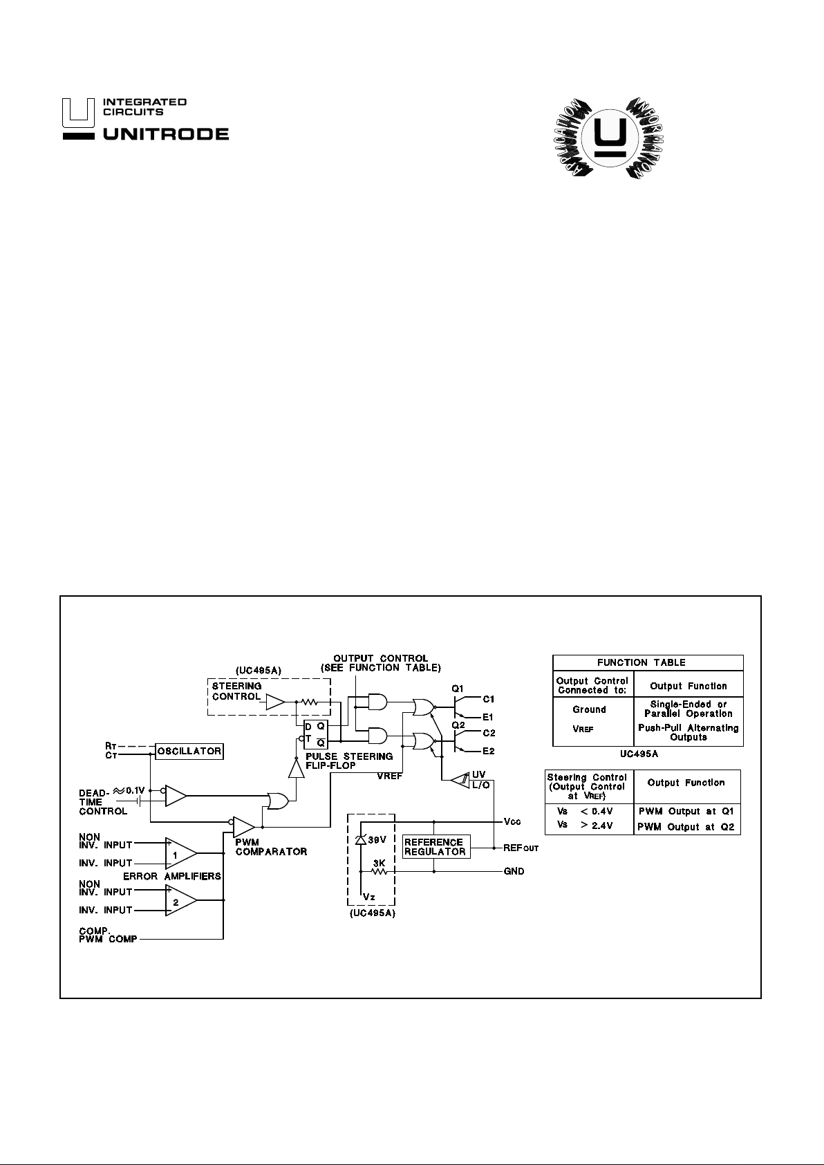
This entire series of PWM modulators each provide a complete pulse width
modulation system in a single monolithic integrated circuit. These devices in -
clude a 5V reference accurate to
±
1%, two independent amplifiers usable for
both voltage and current sensing, an externally synchronizable oscillator
with its linear ramp generator, and two uncommitted transistor output
switches. These two outputs may be operated either in parallel for single-
ended operation or alternatin g for push-pull applications with an externally
controlled d ead-band. These unit s are internally protected agains t double-
pulsing of a si ngle output or from e xtraneous output signals when the input
supply voltage is below minimum.
The UC495A contains an on-chip 39V zener diode for high-voltage applica-
tions where VCC woul d be greater than 40V, and a buffered output steering
control that overrides the internal control of the pulse steering flip-flop.
The UC494A is packaged in a 1 6-pi n DIP, while the UC495A is packaged in
an 18 pin DIP. The UC494A, UC495A are specified for operation over the full
military temperature range of -55°C to +125°C, while the UC494AC,
UC495AC are designed for industrial applications from 0°C to +70°C.
BLOCK DIAGRAM
UC494A/AC
UC495A/AC
10/93
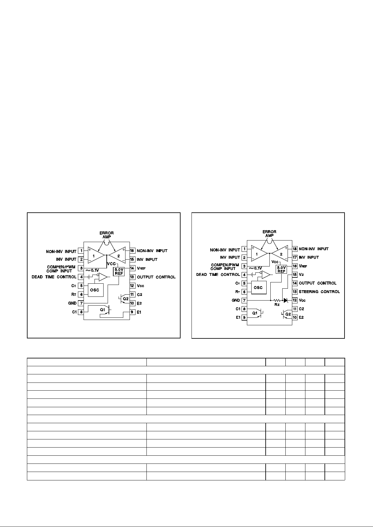
CONNECTION DIAGRAMS
DIL-18 (TOP VIEW)
J or N Package
DIL-18 (TOP VIEW)
J or N Package
UC494A/AC
UC495A/AC
ABSOLUTE MAXI MUM RATING S (Note 1, 2, 3)
Supply Voltage, V CC (Note 2). . . . . . . . . . . . . . . . . . . . . . . . 45V
Amplifier Input Voltages . . . . . . . . . . . . . . . . . . . . . . V
CC + 0.3V
Collector Output Volt age . . . . . . . . . . . . . . . . . . . . . . . . . . . 41V
Collecto r Out put Current. . . . . . . . . . . . . . . . . . . . . . . . . 250mA
Continuous Tot al Diss ip at io n . . . . . . . . . . . . . . . . . . . . 1000mW
@ (or below) 25°C free air temp era tu re range (Note 3)
Storage Temperature Range . . . . . . . . . . . . . . . -65° to +150°C
Lead Temperature 1/16 " (1. 6mm) from case for 60 seconds,
J Package. . . . . . . . . . . . . . . . . . . . . . . . . . . . . . . . . . . 300°C
Lead Temperature 1/16 " (1. 6mm) from case for 10 seconds,
N Package . . . . . . . . . . . . . . . . . . . . . . . . . . . . . . . . . . 260°C
Note 1: Over operat in g free air tempe rat ur e range un le ss
otherwis e noted.
Note 2: All voltage values are with respect to network
ground termina l 3.
Note 3: Consult Packaging Sec tion of Databook r egar ding
thermal specifica tion s and limitat ions of package s.
RECOMMENDED OPERAT ING CONDITI ONS
Supply Voltage V CC . . . . . . . . . . . . . . . . . . . . . . . . . . 7V to 40V
Err or Ampl ifier Input V oltage s . . . . . . . . . . . . . -0.3V to V
CC-2V
Collector Output Volt age . . . . . . . . . . . . . . . . . . . . . . . . . . . 40V
Collector Out put Curren t (each transist or ). . . . . . . . . . . 200mA
Current in to F eedback Term inal. . . . . . . . . . . . . . . . . . . . 0.3mA
Timing Capacit or, C
T . . . . . . . . . . . . . . . . . 0.47nF to 10,000nF
Timing Resistor, R
T . . . . . . . . . . . . . . . . . . . . . 1.8kΩ to 500kΩ
Oscillator Frequency . . . . . . . . . . . . . . . . . . . . 1kHz to 300kHz
Operating Free Air Temperature
UC494A, UC495A . . . . . . . . . . . . . . . . . . . . -55°C to +125°C
UC494AC, UC495AC. . . . . . . . . . . . . . . . . . . . 0°C to +70°C
ELECTRICAL CHARACTERISTICS:
PARAMETER TEST CONDITIONS MIN TYP MAX UNITS
Reference Sec tio n
Output Volt age V
REF IO = 1mA, TA = 25 ° C4.9555.05V
Input Regulation V
CC = 7V to 40V 2 25 mV
Output Regulation I
O = 1mA to 10m A 1 15 mV
Output Voltage O ve r Tempe rat ure ∆T
A = Min. to Max. 4.90 5.10 V
Short Circuit Output Current V
REF = 0, TA = 25°C (Note 1) 10 35 50 mA
Oscillato r Sect io n
Frequency (Not e 2) C
T = 0.01µF, RT = 12kΩ 10 kHz
Standard Deviation Of Freque ncy ( Not e 3) All Values of V
CC, CT, RT, TA Constant 10 %
Frequency Cha nge W ith Voltag e V
CC = 7V to 40V, TA = 25°C0.1%
Frequency Cha nge W ith Tem per ature C
T = 0.01µF, RT = 12kΩ, ∆TA = Min. to Max. 2 %
Deadtime Control Secti on (O u tp ut Cont rol Conn ect ed to V
REF)
Input Bias Curren t (Pin 4) V
(PIN 4) = 0V to 5.25V -2 - 1 0 µA
Maximum Duty-Cycle (Each Output) V
(PIN 4) = 0V 45 %
Unless otherwise stated , ov er recomm end ed ope rat ing fre e-a ir temp era tu re range ,
V
CC = 15V, f = 10kHz, TA = TJ.
UC494A/AC
UC495A/AC
2
 Loading...