


Texas Instruments UC3904N, UC3904DWTR, UC3904DW, UC2904J, UC2904DW Datasheet
...
UC1904
UC2904
UC3904
Precision Quad Supply and Line Monitor
FEATURES
∙Inputs for Monitoring Up to Four Supply Voltages
∙Two Inputs Preset for -5V and -12V Monitoring, or Programmable Positive Levels
∙Precision 2.5V Reference
∙Separate Inputs for Over-Current and Line Fault Sensing
∙Adjustable Underto Over-Voltage Fault Windows
∙Latched Over-Voltage and Over-Current Output
∙Power Good and Power Warning Outputs
∙Auto Restart Function with ON/OFF Control, and Programmable Delay
∙Programmable Pwr On Reset Delay
BLOCK DIAGRAM
DESCRIPTION
The UC1904 Quad Supply Monitor will respond to underand over-volt- age conditions on up to four continuously monitored voltage levels. Four independent positive voltages can be monitored or, alternatively, two of the sense inputs are preset to monitor -5V and -12V supplies. The device also monitors Over-Current and Line Sense inputs, both with precision input thresholds.
Four open collector outputs on the UC1904 give the following responses: 1. The OV/OC output is a latched over-voltage, or over-current response. 2. A Power Good signal responds low with any fault detection
– on power-up a programmable delay is used to hold this output low for a system Power On Reset signal. 3. The PWRW output responds only to a Line Sense input, for early warning of power failures. 4. The last open collector, the ON/OFF output, generates a delayed supply OFF control signal in response to an OFF input command, under-voltage condition, or line fault detection.
The OV-UV fault window is adjustable with a programming input. The thresholds are centered around the precision 2.5V reference, with a scaled hysteresis for precise, glitch free operation. In the positive mode of operation, the fault windows at each of the sense inputs can be independently scaled using external resistors and the 2.5V reference output. An Auto Restart function couples with the under-voltage and line sensing circuits to allow controlled power supply start-up and shutdown.
This device will operate over a supply range of 4.75V to 18V. The device is available in a DIP, SOIC, or PLCC outline. This device is ESD protected on all pins.
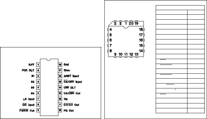
Note: Pin Numbers refer to J, N, and DW Packages.
4/97
ABSOLUTE MAXIMUM RATINGS (Note 1)
Input Supply Voltage . . . . . . . . . . . . . . . . . . . . . . . . . . . . . . 20V Sense Inputs, S1 And S2, Other Analog And Logic Inputs
Maximum Forced Voltage . . . . . . . . . . . . . . . . . . -0.3V to 10V Maximum Forced Current . . . . . . . . . . . . . . . . . . . . . . ±10mA
Sense Input S3, (-12V Sense Input)
Maximum Forced Voltage . . . . . . . . . . . . . . . . . . -18V to 10V Maximum Forced Current . . . . . . . . . . . . . . . . . . . . . . ±10mA
Sense Input S4, (-5V Sense Input)
Maximum Forced Voltage . . . . . . . . . . . . . . . . . . -10V to 10V Maximum Forced Current . . . . . . . . . . . . . . . . . . . . . . ±10mA
Open Collector Outputs
Maximum Voltage . . . . . . . . . . . . . . . . . . . . . . . . . . . . . . . 20V Maximum Current . . . . . . . . . . . . . . . . . . . . . . . . . . . . . 50mA Reference Output Current . . . . . . . . . . . . . . . Internally Limited Operating Junction Temperature . . . . . . . . . . . -55°C to +150°C Storage Temperature . . . . . . . . . . . . . . . . . . . . -65°C to +150°C
DIL-18, SOIC-18 (TOP VIEW)
J or N PACKAGE, DW PACKAGE
UC1904
UC2904
UC3904
Note 1: Unless otherwise indicated, voltages are reference to ground and currents are positive into, negative out of, the specified terminals.
CONNECTION DIAGRAMS
PLCC-20 (TOP VIEW) |
PACKAGE PIN FUNCTION |
|
Q PACKAGE |
||
|
FUNCTION |
PIN |
|
2.5V |
1 |
|
POR DLY |
2 |
|
N.C. |
3 |
|
S1 |
4 |
|
S2 |
5 |
|
S3 |
6 |
|
S4 |
7 |
|
N.C. |
8 |
|
LS Input |
9 |
|
OC Input |
10 |
|
PWRW Out |
11 |
|
PG Out |
12 |
|
OV/OC Out |
13 |
|
VIN |
14 |
|
ON/OFF Out |
15 |
|
OFF DLY |
16 |
|
ON/OFF Input |
17 |
|
ARST Input |
18 |
|
WADJ |
19 |
|
Gnd |
20 |
ELECTRICAL CHARACTERISTICS: Unless otherwise stated, these specifications hold for TA = 0 to 70°C for the |
|
||||||
|
UC3904, -40 to +85°C for the UC2904, and -55 to +125°C for the UC1904, +VIN = |
||||||
|
15V, WADJ = 0.5V, Sense Inputs 1-4, OC and LS Inputs = 2.5V. The ON/OFF Input |
||||||
|
and the ARST Input = 0V. |
|
|
|
|
||
|
|
|
|
|
|
|
|
PARAMETER |
|
TEST CONDITIONS |
MIN |
TYP |
MAX |
UNITS |
|
Input Supply |
|
|
|
|
|
|
|
VIN Supply Current |
VIN = 15V |
|
3.2 |
4.5 |
mA |
||
VIN UVLO Threshold |
Low to High |
|
4.5 |
4.75 |
V |
||
UVLO Threshold Hysteresis |
|
|
|
|
50 |
|
mV |
Minimum VIN to Enable PG Out |
|
|
|
|
0.8 |
1.5 |
V |
Reference |
|
|
|
|
|
|
|
Output Voltage(VREF) |
TJ = 25°C |
2.475 |
2.5 |
2.525 |
V |
||
|
Over Temperature, UC3904 |
2.47 |
|
2.53 |
V |
||
|
Over Temperature, UC2904 & UC1904 |
2.465 |
|
2.535 |
V |
||
Load Regulation |
IOUT = 0 to 4mA |
|
|
6 |
mV |
||
Line Regulation |
VIN = 4.75 to 18V |
|
|
5 |
mV |
||
Short Circuit Current |
VREF = 0V |
|
17 |
|
mA |
||
|
|
|
|
|
|
|
|
OV UV Window, LS Input, OC Input, ARST Input, and |
ON/OFF Input Thresholds |
|
|
|
|
||
Over-Voltage Thresholds |
WADJ = 0.25V, Offset from VREF, Input L to H |
110 |
125 |
140 |
mV |
||
S1, S2 |
WADJ = 0.5V, Offset from VREF, Input L to H |
230 |
250 |
270 |
mV |
||
|
WADJ = 1V, Offset from VREF, Input L to H |
460 |
500 |
540 |
mV |
||
Over-Voltage Thresholds |
WADJ = 0.25V, Offset from VREF, Input L to H |
110 |
125 |
145 |
mV |
||
S3, S4 Positive Mode |
WADJ = 0.5V, Offset from VREF, Input L to H |
230 |
250 |
280 |
mV |
||
|
WADJ = 1V, Offset from VREF, Input L to H |
460 |
500 |
550 |
mV |
||
2
 Loading...