


Texas Instruments UCC3837N, UCC3837DTR, UCC3837D, UCC2837N, UCC2837DTR Datasheet
...
UCC1837 UCC2837 UCC3837
8-Pin N-FET Linear Regulator Controller
FEATURES
•On Board Charge Pump to Drive External N-MOSFET
•Input Voltage as Low as 3V
•Duty Ratio Mode Over Current Protection
•Extremely Low Dropout Voltage
•Low External Parts Count
•Output Voltages as Low as 1.5V
DESCRIPTION
The UCC3837 Linear Regulator Controller includes all the features required for an extremely low dropout linear regulator that uses an external N-channel MOSFET as the pass transistor. The device can operate from input voltages as low as 3V and can provide high current levels, thus providing an efficient linear solution for custom processor voltages, bus termination voltages, and other logic level voltages below 3V. The on board charge pump creates a gate drive voltage capable of driving an external N-MOSFET which is optimal for low dropout voltage and high efficiency. The wide versatility of this IC allows the user to optimize the setting of both current limit and output voltage for applications beyond or between standard 3-terminal linear regulator ranges.
This 8-pin controller IC features a duty ratio current limiting technique that provides peak transient loading capability while limiting the average power dissipation of the pass transistor during fault conditions. See the Application Section for detailed information.
BLOCK DIAGRAM
VDD |
CS |
CAP |
|
|
1 |
8 |
2 |
|
|
|
CHARGE |
LEVEL |
5 |
VOUT |
|
PUMP |
SHIFT |
||
|
|
|
||
|
CURRENT SENSE |
|
|
|
|
AMPLIFIER |
ERROR AMPLIFIER |
|
|
140mV |
|
|
||
|
6 |
FB |
||
|
|
|
||
+ |
|
|
|
|
|
UVLO |
|
|
|
|
CURRENT SENSE |
1.5V REF |
|
|
|
|
|
|
|
|
COMPARATOR |
|
|
|
100mV |
|
3 |
GND |
|
|
TIMER |
|
|
|
+ |
|
|
|
|
|
7 |
4 |
|
|
|
CT |
COMP |
|
UDG-99145 |
SLUS228A - AUGUST 1999 |
|
|
|
|
ABSOLUTE MAXIMUM RATINGS
All pins referenced to GND . . . . . . . . . . . . . . . . . –0.3V to +15V CS, CT, FB . . . . . . . . . . . . . . . . . . . . . . . . –0.3V to VDD + 0.3V Storage Temperature . . . . . . . . . . . . . . . . . . . –65°C to +150°C Junction Temperature. . . . . . . . . . . . . . . . . . . –55°C to +150°C Lead Temperature (Soldering, 10sec.) . . . . . . . . . . . . . +300°C
Currents are positive into, negative out of the specified terminal. Consult Packaging Section of Databook for thermal limitations and considerations of packages.
UCC1837
UCC2837
UCC3837
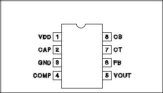
CONNECTION DIAGRAM
DIL-8, SOIC-8 (Top View)
J or N Package, D Package
ELECTRICAL CHARACTERISTICS: Unless otherwise specified, TA = –55°C to 125°C for the UCC1837, –25°C to 85°C for the UCC2837 and 0°C to 70°C for UCC3837; VDD = 5V, C T = 10nF, CCAP = 100nF.
PARAMETER |
TEST CONDITIONS |
MIN |
TYP |
MAX |
UNITS |
Input Supply |
|
|
|
|
|
Supply Current |
VDD = 5V |
|
1 |
1.5 |
mA |
|
VDD = 10V |
|
1.2 |
2 |
mA |
Under Voltage Lockout |
|
|
|
|
|
Minimum Voltage to Start |
|
2.00 |
2.65 |
3.00 |
V |
Minimum Voltage After Start |
|
1.6 |
2.2 |
2.6 |
V |
Hysteresis |
|
0.25 |
0.45 |
0.65 |
V |
Reference ( Note 1 ) |
|
|
|
|
|
VREF |
25°C |
1.485 |
1.5 |
1.515 |
V |
|
0°C to 70°C |
1.470 |
1.5 |
1.530 |
V |
|
–55°C to 125°C |
1.455 |
1.5 |
1.545 |
V |
Current Sense |
|
|
|
|
|
Comparator Offset |
0°C to 70°C |
90 |
100 |
110 |
mV |
Comparator Offset |
–55°C to 125°C |
85 |
100 |
115 |
mV |
Amplifier Offset |
|
120 |
140 |
160 |
mV |
Input Bias Current |
VCS = 5V |
|
0.5 |
5 |
A |
Current Fault Timer |
|
|
|
|
|
CT Charge Current |
VCT = 1V |
16 |
36 |
56 |
A |
CT Discharge Current |
VCT = 1V |
0.4 |
1.2 |
1.9 |
A |
CT Fault Low Threshold |
|
0.4 |
0.5 |
0.6 |
V |
CT Fault Hi Threshold |
|
1.3 |
1.5 |
1.7 |
V |
Fault Duty Cycle |
|
2 |
3.3 |
5 |
% |
Error Amplifier |
|
|
|
|
|
Input Bias Current |
|
|
0.5 |
2 |
A |
Open Loop Gain |
|
60 |
90 |
|
dB |
Transconductance |
–10 A to 10 A |
2 |
5 |
8 |
mMho |
Charge Current |
VCOMP = 6V |
20 |
40 |
60 |
A |
Discharge Current |
VCOMP = 6V |
10 |
25 |
40 |
A |
2

UCC1837
UCC2837
UCC3837
ELECTRICAL CHARACTERISTICS: Unless otherwise specified, TA = –55°C to 125°C for the UCC1837, –25°C to 85°C for the UCC2837 and 0°C to 70°C for UCC3837; VDD = 5V, C T = 10nF, CCAP = 100nF.
PARAMETER |
TEST CONDITIONS |
MIN |
TYP |
MAX |
UNITS |
FET Driver |
|
|
|
|
|
Peak Output Current |
VCAP = 10V, VOUT = 1V |
0.5 |
1.5 |
2.5 |
mA |
Average Output Current |
VOUT = 1V |
25 |
100 |
175 |
A |
Max Output Voltage |
VDD = 4.5V, IOUT = 0 A |
8.4 |
9.7 |
|
V |
|
VDD = 4.5V, IOUT = 10 A, 0°C to 70°C |
8 |
9 |
|
V |
|
VDD = 4.5V, IOUT = 10 A, –55°C to 125°C |
7.5 |
9 |
|
V |
Charge Pump |
|
|
|
|
|
CAP Voltage |
VDD = 4.5V, C/S = 0V |
11 |
12.5 |
|
V |
|
VDD = 12V, C/S = 0V |
|
15 |
16.5 |
V |
Note 1: This is defined as the voltage on FB which results in a DC voltage of 8V on VOUT.
PIN DESCRIPTIONS
CAP: The output of the charge pump circuit. A capacitor is connected between this pin and GND to provide a floating bias voltage for an N-Channel MOSFET gate drive. A minimum of a 0.01µ F ceramic capacitor is recommended. CAP can be directly connected to an external regulated source such as +12V, in which case the external voltage will be the source for driving the N-Channel MOSFET.
COMP: The output of the transconductance error amplifier and current sense amplifier. Used for compensating the small signal characteristics of the voltage loop (and current loop when Current Sense Amplifier is active in over curret mode).
CS: The negative current sense input signal. This pin should be connected through a low noise path to the low side of the current sense resistor.
CT: The input to the duty cycle timer circuit. A capacitor is connected from this pin to GND, setting the maximum ON time of the over current protection circuits. See the Application Section for programming instructions.
FB: The inverting terminal of the voltage error amplifier, used to feedback the output voltage for comparison with the internal reference voltage. The nominal DC operating voltage at this pin is 1.5V
GND: Ground reference for the device. For accurate output voltage regulation, GND should be referenced to the output load ground.
VDD: The system input voltage is connected to this point. VDD must be above 3V. VDD also acts as one side of the Current Sense Amplifier and Comparator.
VOUT: This pin directly drives the gate of the external N-MOSFET pass element. The typical output impedance of this pin is 6.5kΩ .
APPLICATION INFORMATION
Topology and General Operation
Unitrode Application Note U-152 is a detailed design of a low dropout linear regulator using an N-channel MOSFET as a pass element, and should be used as a guide for understanding the operation of the circuit shown in Fig. 1.
Charge Pump Operation
The internal charge pump of the UCC3837 is designed to create a voltage equal to 3 times the input VDD voltage at the CAP pin. There is an internal 5V clamp at the input of the charge pump however that insures the voltage at CAP does not exceed the ratings of the IC. This CAP voltage is used to provide gate drive current to the external pass element as well as bias current to internal sec-
tions of the UCC3837 itself. The charge pump output has a typical impedance of 80kΩ and therefore the loading of the IC and the external gate drive reduces the voltage from its ideal level. The UCC3837 can operate in several states including having the error amplifier disabled (shut down), in normal linear regulation mode, and in overdrive mode where the linear regulator is responding to a transient load or line condition. The maximum output voltage available at VOUT is shown in Fig. 2 for these various modes of operation.
The charge pump output is designed to supply 10µ A of average current to the load which is typically the MOSFET gate capacitance present at the VOUT pin.The capacitor value used at CAP is chosen to provide holdup
3
 Loading...