


Texas Instruments UC3855BN, UC3855BDWTR, UC3855BDW, UC3855AN, UC3855ADWTR Datasheet
...
UC1855A/B
UC2855A/B
UC3855A/B
High Performance Power Factor Preregulator 

FEATURES
∙Controls Boost PWM to Near Unity Power Factor
∙Fixed Frequency Average Current Mode Control Minimizes Line Current Distortion
∙Built-in Active Snubber (ZVT) allows Operation to 500kHz, improved EMI and Efficiency
∙Inductor Current Synthesizer allows Single Current Transformer Current Sense for Improved Efficiency and Noise Margin
∙Accurate Analog Multiplier with Line Compensator allows for Universal Input Voltage Operation
∙High Bandwidth (5MHz), Low Offset Current Amplifier
∙Overvoltage and Overcurrent protection
∙Two UVLO Threshold Options
∙150μA Startup Supply Current Typical
∙Precision 1% 7.5V Reference
BLOCK DIAGRAM
DESCRIPTION
The UC1855A/B provides all the control features necessary for high power, high frequency PFC boost converters. The average current mode control method allows for stable, low distortion AC line current programming without the need for slope compensation. In addition, the UC1855 utilizes an active snubbing or ZVT (Zero Voltage Transition technique) to dramatically reduce diode recovery and MOSFET turn-on losses, resulting in lower EMI emissions and higher efficiency. Boost converter switching frequencies up to 500kHz are now realizable, requiring only an additional small MOSFET, diode, and inductor to resonantly soft switch the boost diode and switch. Average current sensing can be employed using a simple resistive shunt or a current sense transformer. Using the current sense transformer method, the internal current synthesizer circuit buffers the inductor current during the switch on-time, and reconstructs the inductor current during the switch off-time. Improved signal to noise ratio and negligible current sensing losses make this an attractive solution for higher power applications.
The UC1855A/B also features a single quadrant multiplier, squarer, and divider circuit which provides the programming signal for the current loop. The internal multiplier current limit reduces output power during low line conditions. An overvoltage protection circuit disables both controller outputs in the event of a boost output OV condition.
Low startup supply current, UVLO with hysteresis, a 1% 7.5V reference, voltage amplifier with softstart, input supply voltage clamp, enable comparator, and overcurrent comparator complete the list of features. Available packages include: 20 pin N, DW, Q, J, and L.
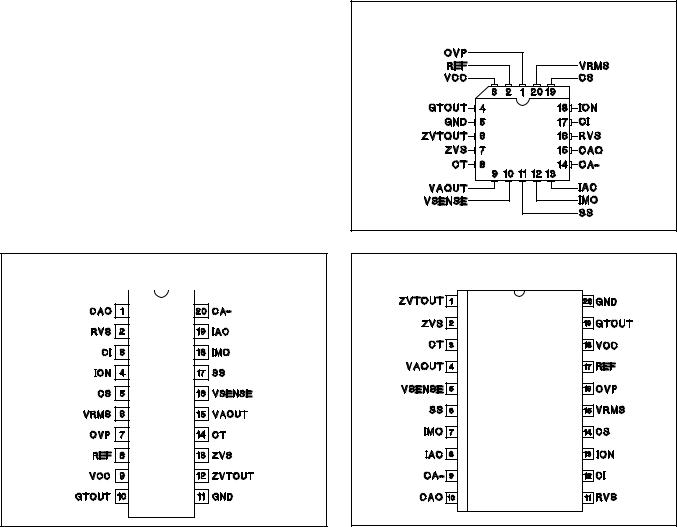
License Patent from Pioneer Magnetics. Pin numbers refer to DIL-20 J or N packages.
6/98
UDG-94001-2
UC1855A/B
UC2855A/B
UC3855A/B
ABSOLUTE MAXIMUM RATINGS |
CONNECTION DIAGRAMS |
Supply Voltage VCC. . . . . . . . . . . . . . . . . . . . . . . . . . Internally Limited VCC Supply Clamp Current . . . . . . . . . . . . . . . . . . . . . . . 20mA PFC Gate Driver Current (continuous) . . . . . . . . . . . . . . ± 0.5A PFC Gate Driver Current (peak) . . . . . . . . . . . . . . . . . . . ± 1.5A ZVT Drive Current (continuous) . . . . . . . . . . . . . . . . . . . ± 0.25A ZVT Drive Current (peak) . . . . . . . . . . . . . . . . . . . . . . . ± 0.75A Input Current (IAC, RT, RVA) . . . . . . . . . . . . . . . . . . . . . . . 5mA Analog Inputs (except Peak Limit). . . . . . . . . . . . . . −0.3 to 10V Peak Limit Input . . . . . . . . . . . . . . . . . . . . . . . . . . . −0.3 to 6.5V Softstart Sinking Current . . . . . . . . . . . . . . . . . . . . . . . . . 1.5mA Storage Temperature . . . . . . . . . . . . . . . . . . . −65°C to +150 °C Junction Temperature . . . . . . . . . . . . . . . . . . . −55°C to +150 °C Lead Temperature (Soldering, 10 sec.) . . . . . . . . . . . . . +300°C
Currents are positive into, negative out of the specified terminal. Consult Packaging Section of Databook for thermal limitations and considerations of packages. All voltages are referenced to GND.
DIL–20 (Top View)
J or N Package
PLCC-20 & LCC-20 (Top View) Q or L Package
SOIC-20 (Top View)
DW Package
ELECTRICAL CHARACTERISTICS: Unless otherwise specified: VCC = 18V, RT = 15k, RVS = 23k, CT = 470pF, CI =
150pF, VRMS = 1.5V, IAC = 100μA, ISENSE = 0V, CAOUT = 4V, VAOUT= 3.5V, VSENSE = 3V. TA = TJ. TA = –55°C to 125°C (UC1855A/B), –40°C to 85°C (UC2855A/B), 0 °C to 70°C (UC3855A/B).
PARAMETER |
TEST CONDITIONS |
MIN |
TYP |
MAX |
UNITS |
Overall |
|
|
|
|
|
Supply Current, OFF |
CAO, VAOUT = 0V, VCC = UVLO −0.3V |
|
150 |
500 |
μA |
Supply Current, OPERATING |
|
|
17 |
25 |
mA |
VCC Turn-On Threshold |
UC1855A |
|
15.5 |
17.5 |
V |
VCCTurn-Off Threshold |
UC1855A,B |
9 |
10 |
|
V |
VCC Turn-On Threshold |
UC1855B |
|
10.5 |
10.8 |
V |
VCC Clamp |
I(VCC) = ICC(on) + 5mA |
18 |
20 |
22 |
V |
Voltage Amplifier |
|
|
|
|
|
Input Voltage |
|
2.9 |
|
3.1 |
V |
VSENSE Bias Current |
|
−500 |
25 |
500 |
nA |
Open Loop Gain |
VOUT = 2 to 5V |
65 |
80 |
|
dB |
VOUT High |
ILOAD = –300μA |
5.75 |
6 |
6.25 |
V |
VOUT Low |
ILOAD = 300μA |
|
0.3 |
0.5 |
V |
Output Short Circuit Current |
VOUT = 0V |
|
0.6 |
3 |
mA |
2
UC1855A/B
UC2855A/B
UC3855A/B
ELECTRICAL CHARACTERISTICS: Unless otherwise specified: VCC = 18V, RT = 15k, RVS = 23k, CT = 470pF, CI =
150pF, VRMS = 1.5V, IAC = 100μA, ISENSE = 0V, CAOUT = 4V, VAOUT= 3.5V, VSENSE = 3V. TA = TJ. TA = –55°C to 125°C (UC1855A/B), –40°C to 85°C (UC2855A/B), 0 °C to 70°C (UC3855A/B).
PARAMETER |
TEST CONDITIONS |
MIN |
TYP |
MAX |
UNITS |
Current Amplifier |
|
|
|
|
|
Input Offset Voltage |
VCM = − 2.5V |
−4 |
|
4 |
mV |
Input Bias Current (Sense) |
VCM = 2.5V |
−500 |
|
500 |
nA |
Open Loop Gain |
VCM = 2.5V, VOUT = 2 to 6V |
80 |
110 |
|
dB |
VOUT High |
ILOAD = −500μA |
|
6 |
|
V |
VOUT Low |
ILOAD = 500μA |
|
0.3 |
0.5 |
V |
Output Short Circuit Current |
VOUT = 0V |
|
1 |
3 |
mA |
Common Mode Range |
|
−0.3 |
|
5 |
V |
Gain Bandwidth Product |
FIN = 100kHz, 10mV, P–P, TA = 25°C |
2.5 |
5 |
|
MHz |
Reference |
|
|
|
|
|
Output Voltage |
IREF = 0mA, TA = 25°C |
7.388 |
7.5 |
7.613 |
V |
|
IREF = 0mA |
7.313 |
7.5 |
7.688 |
V |
Load Regulation |
IREF = 1 to 10 mA |
−15 |
|
15 |
mV |
Line Regulation |
VCC = 15 to 35V |
−10 |
|
10 |
mV |
Short Circuit Current |
REF = 0V |
20 |
45 |
65 |
mA |
Oscillator |
|
|
|
|
|
Initial Accuracy |
TA = 25°C |
170 |
200 |
230 |
kHz |
Voltage Stability |
VCC = 12 to 18V |
|
1 |
|
% |
Total Variation |
Line, Temp. |
160 |
|
240 |
kHz |
Ramp Amplitude (P–P) |
|
4.9 |
|
5.9 |
V |
Ramp Valley Voltage |
|
1.1 |
|
1.6 |
V |
Enable/OVP/Current Limit |
|
|
|
|
|
Enable Threshold |
|
|
1.8 |
2.2 |
V |
OVP Threshold |
|
|
7.5 |
7.66 |
V |
OVP Hysteresis |
|
200 |
400 |
600 |
mV |
OVP Propagation Delay |
|
|
200 |
|
ns |
OVP Input Bias Current |
V= 7.5V |
|
1 |
10 |
μA |
PKLIMIT Threshold |
|
1.25 |
1.5 |
1.75 |
V |
PKLIMIT Input Current |
VPKLIMIT = 1.5V |
|
100 |
|
μA |
PKLIMIT Prop. Delay |
|
|
100 |
|
ns |
Multiplier |
|
|
|
|
|
Output Current - IAC Limited |
IAC = 100μA, VRMS = 1V |
−235 |
−205 |
−175 |
μA |
Output Current - Zero |
IAC = 0μA |
−2 |
−0.2 |
2 |
μA |
Output Current - Power Limited |
VRMS = 1.5V, VAOUT = 5.5V |
−250 |
−209 |
−160 |
μA |
Output Current |
VRMS = 1.5V, VAOUT = 2V |
|
−26 |
|
μA |
|
VRMS = 1.5V VAOUT = 5V |
|
−190 |
|
μA |
|
VRMS = 5V, VAOUT = 2V |
|
−3 |
|
μA |
|
VRMS = 5V, VAOUT = 5V |
|
−17 |
|
μA |
Gain Constant |
Refer to Note 1 |
−0.95 |
−0.85 |
−0.75 |
1/V |
Gate Driver Output |
|
|
|
|
|
Output High Voltage |
lOUT = −200mA, VCC = 15V |
12 |
12.8 |
|
V |
Output Low Voltage |
lOUT = 200mA |
|
1 |
2.2 |
V |
Output Low Voltage |
lOUT = 10mA |
|
300 |
500 |
mV |
Output Low (UVLO) |
lOUT = 50mA, VCC = 0V |
|
0.9 |
1.5 |
V |
Output RISE/FALL Time |
CLOAD = 1nF |
|
35 |
|
ns |
Output Peak Current |
CLOAD = 10nF |
|
1.5 |
|
A |
3
 Loading...