


Texas Instruments UCC381DPTR-ADJ, UCC381DPTR-5, UCC381DP-ADJ, UCC381DP-5, UCC381DP-3 Datasheet
...
UCC281-3/-5/-ADJ
UCC381-3/-5/-ADJ
Low Dropout 1 Ampere Linear Regulator Family
FEATURES
•Precision Positive Linear Voltage Regulation
•0.5V Dropout at 1A
•Guaranteed Reverse Input/ Output Voltage Isolation with Low Leakage
•Low Quiescent Current Irrespective of Load
•Adjustable Output Voltage Version
•Fixed Versions for 3.3V and 5V Outputs
•Logic Shutdown Capability
•Short Circuit Power Limit of 3% • VIN • Current Limit
•Remote Load Voltage for Accurate Load Regulation
DESCRIPTION
The UCC381-3/-5/-ADJ family of positive linear series pass regulators is tailored for low drop out applications where low quiescent power is important. Fabricated with a BiCMOS technology ideally suited for low input to output differential applications, the UCC381 will pass 1A while requiring only 0.5V of input voltage headroom. Dropout voltage decreases linearly with output current, so that dropout at 200mA is less than 100mV. Quiescent current is always less than 650 A. To prevent reverse current conduction, on-chip circuitry limits the minimum forward voltage to typically 50mV. Once the forward voltage limit is reached, the input-output differential voltage is maintained as the input voltage drops until undervoltage lockout disables the regulator.
UCC381-3 and UCC381-5 versions have on-chip resistor networks preset to regulate either 3.3V or 5.0V, respectively. Furthermore, remote sensing of the load voltage is possible by connecting the VOUTS pin directly at the load. The output voltage is then regulated to 1.5% at room temperature and better than 2.5% over temperature. The UCC381-ADJ version has a regulated output voltage programmed by an external user-definable resistor ratio.
(continued)
BLOCK DIAGRAM
VIN |
8 |
|
|
|
|
|
1 |
VOUT |
|
|
|
|
VPUMP |
|
|
4 |
VOUTS |
|
|
|
|
|
|
|
||
|
|
|
CURRENT |
|
VOLTAGE |
|
R2 |
|
|
|
|
|
AMPLIFIER |
|
|
||
|
|
|
LIMIT |
|
|
|
|
|
|
|
|
|
|
|
|
|
|
|
|
|
– |
|
– |
|
|
|
|
1.3/2.1A |
|
+ |
|
|
|
||
|
+ |
|
|
|
|
|||
|
CURRENT |
|
|
|
2 |
GND |
||
|
REFERENCE |
|
|
|
|
|||
|
|
|
|
|
|
|
||
|
|
|
|
|
|
1.25V |
3 |
GND |
|
SHUTDOWN FOR FIXED VERSIONS |
|
|
|
||||
|
|
|
|
R1 |
|
|||
|
|
|
|
|
|
|
|
|
CT* |
5 |
|
|
|
|
|
6 |
GND |
|
|
0.65V |
|
|
|
|
7 |
GND |
|
|
|
|
|
|
|
||
|
|
3% DUTY CYCLE |
|
|
|
|
|
|
|
*ADJ |
CURRENT LIMIT TIMER |
|
|
|
|
|
|
|
|
|
|
|
|
|
|
|
|
VERSION |
|
|
|
|
R2 |
R1 |
|
|
ONLY |
REVERSE VOLTAGE |
|
|
|
|||
|
|
|
SENSE |
|
UCC381-ADJ |
0 |
OPEN |
|
|
|
|
|
|
|
|||
|
|
|
|
UVLO |
UCC381-3 |
82k |
50k |
|
|
|
|
THERMAL |
|
|
|||
|
|
|
|
|
|
|
|
|
|
|
|
SHUTDOWN |
|
UCC381-5 |
150k |
50k |
|
UDG-98112
SLUS214A - NOVEMBER 1999
ABSOLUTE MAXIMUM RATINGS
VIN. . . . . . . . . . . . . . . . . . . . . . . . . . . . . . . . . . . . . . . . . . . . . 9V CT . . . . . . . . . . . . . . . . . . . . . . . . . . . . . . . . . . . . . . . −0.3 to 3V Storage Temperature . . . . . . . . . . . . . . . . . . . −65°C to +150°C Junction Temperature. . . . . . . . . . . . . . . . . . . −55°C to +150°C Lead Temperature (Soldering, 10 sec.) . . . . . . . . . . . . . +300°C
Currents are positive into, negative out of the specified terminal. Consult Packaging Section of Databook for thermal limitations and considerations of packages. All voltages are referenced to GND.
DESCRIPTION (cont.)
UCC281-3/-5/-ADJ
UCC381-3/-5/-ADJ
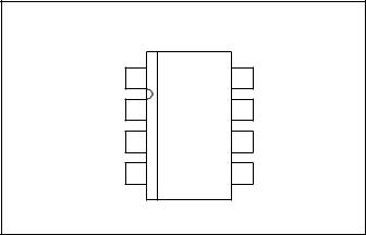
CONNECTION DIAGRAMS
SOIC-8 (Top View)
DP Package
VOUT |
1 |
8 |
VIN |
GND |
2 |
7 |
GND |
GND |
3 |
6 |
GND |
VOUTS |
4 |
5 |
CT* |
* ADJ version only
Short circuit current is internally limited. The device responds to a sustained overcurrent condition by turning off after a TON delay. The device then stays off for a pe-
riod, TOFF, that is 32 times the TON delay. The device then begins pulsing on and off at the TON /(TON+TOFF) duty cycle of 3%. This drastically reduces the power dis-
sipation during short circuit such that heat sinking, if at all required, must only accommodate normal operation. On the fixed output versions of the device TON is fixed at 400µs − a guaranteed minimum. On the adjustable version an external capacitor sets the on time. The off time is always 32 times TON.
The UCC381 can be shutdown to 25µA (max) by pulling the CT pin low.
Internal power dissipation is further controlled with thermal overload protection circuitry. Thermal shutdown occurs if the junction temperature exceeds 165°C. The chip will remain off until the temperature has dropped 20°C.
The UCC281 series is specified for operation over the industrial range of −40°C to +85°C, and the UCC381 series is specified from 0°C to +70°C. These devices are available in the 8 pin DP surface mount power package. For other packaging options consult the factory.
ELECTRICAL CHARACTERISTICS: Unless otherwise stated, these specifications hold for TA = 0°C to 70°C for the
UCC381-X series and −40°C to +85°C for the UCC283-X series, VIN = VOUT + 1.5V, IOUT = 0mA, COUT = 2.2µF. CT = 1500pF for the UCC381-ADJ version and VOUT set to 5V. TJ = TA.
PARAMETER |
TEST CONDITIONS |
MIN |
TYP |
MAX |
UNITS |
UCC381-5 Fixed 5V, 1A Family |
|
|
|
|
|
Output Voltage |
TJ = 25°C |
4.925 |
5 |
5.075 |
V |
|
Over Temperature |
4.875 |
|
5.125 |
V |
Line Regulation |
VIN = 5.15V to 9V |
|
1 |
3 |
mV |
Load Regulation |
IOUT = 0mA to 1A |
|
2 |
5 |
mV |
Drop Out Voltage, VIN – VOUT |
IOUT = 1A, VOUT = 4.85V, TA < 85°C |
|
0.5 |
0.6 |
V |
|
IOUT = 200mA, VOUT = 4.85V, TA < 85°C |
|
100 |
200 |
mV |
Peak Current Limit |
VOUT = 0V |
|
2 |
3.5 |
A |
Overcurrent Threshold |
|
1 |
|
1.8 |
A |
Current Limit Duty Cycle |
VOUT = 0V |
|
3 |
5 |
% |
Overcurrent Time Out, TON |
VOUT = 0V |
400 |
750 |
1600 |
µs |
Quiescent Current |
|
|
400 |
650 |
µA |
Quiescent Current in Shutdown |
VIN = 9V |
|
10 |
25 |
µA |
Shutdown Threshold |
At CT Input |
0.25 |
0.65 |
|
V |
Reverse Leakage Current |
1V < VIN < VOUT, VOUT < 5.1V, at VOUT |
|
|
75 |
µA |
UVLO Threshold |
VIN where VOUT passes current |
2.5 |
2.8 |
3.0 |
V |
2
UCC281-3/-5/-ADJ
UCC381-3/-5/-ADJ
ELECTRICAL CHARACTERISTICS: Unless otherwise stated, these specifications hold for TA = 0°C to 70°C for the
UCC381-X series and −40°C to +85°C for the UCC283-X series, VIN = VOUT + 1.5V, IOUT = 0mA, COUT = 2.2µF. CT = 1500pF for the UCC381-ADJ version and VOUT set to 5V. TJ = TA.
PARAMETER |
TEST CONDITIONS |
MIN |
TYP |
MAX |
UNITS |
UCC381-3 Fixed 3.3V, 1A Family |
|
|
|
|
|
Output Voltage |
TJ = 25°C |
3.25 |
3.3 |
3.35 |
V |
|
Over Temperature |
3.22 |
|
3.38 |
V |
Line Regulation |
VIN = 3.45V to 9V |
|
1 |
3 |
mV |
Load Regulation |
IOUT = 0mA to 1A |
|
2 |
5 |
mV |
Dropout Voltage, VIN - VOUT |
IOUT = 1A, VOUT = 3.15V, TA < 85°C |
|
0.6 |
0.8 |
V |
|
IOUT = 200mA, VOUT = 3.15V, TA < 85°C |
|
100 |
200 |
mV |
Peak Current Limit |
VOUT = 0V |
|
2 |
3.5 |
A |
Overcurrent Threshold |
|
1 |
|
1.8 |
A |
Current Limit Duty Cycle |
VOUT = 0V |
|
3 |
5 |
% |
Overcurrent Time Out, TON |
VOUT = 0V |
400 |
750 |
1600 |
µs |
Quiescent Current |
|
|
400 |
650 |
µA |
Quiescent Current in Shutdown |
VIN = 9V |
|
10 |
25 |
µA |
Shutdown Threshold |
At CT Input |
0.25 |
0.65 |
|
V |
Reverse Leakage Current |
1V < VIN < VOUT, VOUT < 3.35V, at VOUT |
|
|
75 |
µA |
UVLO Threshold |
VIN where VOUT passes current |
2.5 |
2.8 |
3.0 |
V |
UCC381-ADJ Adjustable Output, 1A Family |
|
|
|
|
|
Regulating Voltage at ADJ Input |
TJ = 25°C |
1.23 |
1.25 |
1.27 |
V |
|
Over Temperature |
1.22 |
|
1.28 |
V |
Line Regulation, at ADJ Input |
VIN = VOUT + 150mV to 9V |
|
1 |
3 |
mV |
Load Regulation, at ADJ Input |
IOUT = 0mA to 1A |
|
2 |
5 |
mV |
Dropout Voltage, VIN - VOUT |
IOUT = 1A, VOUT = 4.85V |
|
0.5 |
0.6 |
V |
|
IOUT = 200mA, VOUT = 4.85V |
|
100 |
200 |
mV |
Peak Current Limit |
VOUT = 0V |
|
2 |
3.5 |
A |
Overcurrent Threshold |
|
1 |
|
1.8 |
A |
Current Limit Duty Cycle |
VOUT = 0V |
|
3 |
5 |
% |
Overcurrent Time Out, TON |
VOUT = 0V, CT = 1500pF |
400 |
1000 |
1600 |
µs |
Quiescent Current |
|
|
400 |
650 |
µA |
Quiescent Current in Shutdown |
VIN = 9V |
|
10 |
25 |
µA |
Shutdown Threshold |
At CT Input |
0.25 |
0.65 |
|
V |
Reverse Leakage Current |
1V < VIN < VOUT, VOUT < 9V, at VOUT |
|
|
100 |
µA |
Bias Current at ADJ Input |
|
|
100 |
250 |
nA |
UVLO Threshold |
VIN where VOUT passes current |
2.5 |
2.8 |
3.0 |
V |
3
 Loading...